EP0088548A2 - Piezoelektrische Resonatoren - Google Patents
Piezoelektrische Resonatoren Download PDFInfo
- Publication number
- EP0088548A2 EP0088548A2 EP83300872A EP83300872A EP0088548A2 EP 0088548 A2 EP0088548 A2 EP 0088548A2 EP 83300872 A EP83300872 A EP 83300872A EP 83300872 A EP83300872 A EP 83300872A EP 0088548 A2 EP0088548 A2 EP 0088548A2
- Authority
- EP
- European Patent Office
- Prior art keywords
- axis
- resonance chip
- resonance
- chip
- piezoelectric resonator
- Prior art date
- Legal status (The legal status is an assumption and is not a legal conclusion. Google has not performed a legal analysis and makes no representation as to the accuracy of the status listed.)
- Granted
Links
Images





Classifications
-
- H—ELECTRICITY
- H03—ELECTRONIC CIRCUITRY
- H03H—IMPEDANCE NETWORKS, e.g. RESONANT CIRCUITS; RESONATORS
- H03H9/00—Networks comprising electromechanical or electro-acoustic elements; Electromechanical resonators
- H03H9/02—Details
- H03H9/02007—Details of bulk acoustic wave devices
- H03H9/02015—Characteristics of piezoelectric layers, e.g. cutting angles
- H03H9/02031—Characteristics of piezoelectric layers, e.g. cutting angles consisting of ceramic
-
- H—ELECTRICITY
- H03—ELECTRONIC CIRCUITRY
- H03H—IMPEDANCE NETWORKS, e.g. RESONANT CIRCUITS; RESONATORS
- H03H9/00—Networks comprising electromechanical or electro-acoustic elements; Electromechanical resonators
- H03H9/02—Details
- H03H9/02007—Details of bulk acoustic wave devices
- H03H9/02157—Dimensional parameters, e.g. ratio between two dimension parameters, length, width or thickness
-
- H—ELECTRICITY
- H03—ELECTRONIC CIRCUITRY
- H03H—IMPEDANCE NETWORKS, e.g. RESONANT CIRCUITS; RESONATORS
- H03H9/00—Networks comprising electromechanical or electro-acoustic elements; Electromechanical resonators
- H03H9/15—Constructional features of resonators consisting of piezoelectric or electrostrictive material
- H03H9/17—Constructional features of resonators consisting of piezoelectric or electrostrictive material having a single resonator
- H03H9/177—Constructional features of resonators consisting of piezoelectric or electrostrictive material having a single resonator of the energy-trap type
Definitions
- the present invention relates to piezoelectric resonates, more particularly to a piezoelectric resonator comprising a substantially X-cut plate of lithium tantalate (LiTa0 3 ) crystal.
- a piezoelectric resonator comprises a plate of piezo-electric material such as crystal or lithium tantalate and an electrode film coated upon the upper and lower main surfaces of the plate.
- an alternating (a.c.) electric field is applied between the electrode films, the piezo-electric plate is subject to stress of a frequency equal to that of the a.c. electric field.
- Such a vibrating stress mode is called thickness shear.
- Oscillating devices comprising such piezoelectric resonators are widely used in oscillators or filters of communication apparatus due to their compactness, high reliability, and high stability of oscillation frequency.
- single-mode resonators in which suprious responses are eliminated are desired, and also multi-mode filters, wherein the oscillation energy is trapped or concentrated in the vicinity of the electrodes by the mass load effect and the piezoelectric reaction.
- An embodiment of the present invention can provide a piezoelectric resonator of thickness shear mode comprising a bar-like resonance chip made of an X-cut plate of lithium tantalate crystal and having a rectangular cross-section.
- An electrode film is formed at the center portion of the chip with respect to the longitudinal direction on each of two surfaces parallel to the X-plane (i.e., the plane perpendicular to the X-axis of the crystal) of the chip.
- the width of the electrode is equal to the width of the chip.
- the longitudinal direction of the chip inclines with respect to the Y-axis by an angle of-50° + 2° (in the anticlockwise direction) in the X-plane so as to make the longitudinal direction of he chip coincide with the oscillating direction of the main oscillation of the crystal.
- the X-cut plate is a crystal plate which is perpendicular to the X-axis of the crystal.
- Such an X-cut plate includes a plate which is rotated about the Y-axis and/or Z-axis of the crystal.
- Such a resonator can have high electromechanical coupling.
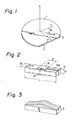
- a wafer 1 illustrated in Fig. 1 is formed by cutting a crystal of lithium tantalate.
- the wafer 1 is an X-cut plate, i.e., a plate whose main surfaces are perpendicular to the X-axis of the crystal.
- the crystal of the X-cut plate may be rotated about the Y-axis and/or Z-axis.
- the wafer 1 has an edge 2 for positioning the wafer 1 at the time of cutting.
- the edge 2 is perpendicular to the Z-axis so that the wafer 1 can be easily positioned at a desired angle with respect to the crystal orientation.
- the Y-axis is parallel to the edge 2.
- a number of resonance chips 3 of a longitudinal box shape are cut from the wafer 1 in the same longitudinal direction.
- a pair of electrodes 4, 4' (Fig. 2) are formed on the X planes, i.e., the planes perpendicular to the X-axis, of the bar-shaped resonance chip 3.
- the width of the electrode is equal to the width of the resonance chip.
- the upper electrode 4 is connected to a terminal (not shown) at an end of the resonance chip 3 through a lead 4a.
- the lower electrode 4' is connected to another terminal (not shown) at the other end of the resonance chip 3 through another lead.
- Length L, width W, and thickness H of the rectangular--strip-shaped resonance chip 3 are determined as follows. Width W is made about 1.5 times larger than thickness H so that unnecessary responses generated within the resonance chip 3 do not affect the resonance of-thickness shear mode. Width of the electrode 4 is made equal to the width W of the resonance chip 3 to equalize the energy of resonance in the transverse direction of the resonance chip 3 and prevent waves reflected from the sides of the resonance chip 3 from affecting the primary resonance oscillation. Since the width of the resonance chip 3 need only be the same as the width of the electrode 4, the resonator may be made narrow in width, and compact.
- length L be more than 10 times larger than thickness H so that the energy of oscillation is efficiently concentrated and trapped between the pair of electrodes 4, 4' disposed at the center of the resonance chip 3.
- energy which is transmitted to the ends of the chip can be minimized so that waves reflected upon the end surfaces of the resonance chip 3 do not affect the main resonance.
- the resonance chip 3 can be held at the ends thereof since the acoustic energy is minimized there.
- the thickness shear mode resonances in the X-cut plate comprises a fast mode and a slow mode.
- the displacement directions of the fast and the slow shear waves are perpendicular to each other and constant with respect to the Y-axis of the crystal.
- the shear wave of the fast mode is used as the main resonance since the electro-mechanical coupling of the fast mode is very large.
- the orientation of the crystal of the resonance chip 3 is arranged so that the direction of the fast mode (shown by arrows in Fig. 2) coincides with the longitudinal direction of the chip 3. That is, the cutting direction of the resonance chip 3 in the wafer 1 is determined so that the angle ⁇ (Fig. 1) between the Y-axis and the longitudinal direction of the chip 3 is equal to the constant angle between the Y-axis and the displacement direction of the thickness shear mode of the fast mode.
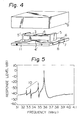
- angle ⁇ in Fig. 1 The angle between Y-axis and the displacement direction of the thickness shear mode of the piezoelectric resonator of the X-cut plate of lithium tantalate, i.e., angle ⁇ in Fig. 1, has been previously proposed to be -53° (NDK technical report No. 6 '79, 11 "Oscillator Controlled by Electric Voltage Using Lithium Tantalate Resonator", Nippon Dempa Kogyo). However, the resonance chip of this angle generates spurious response 10 as can be seen in the graph of frequency characteristic of Fig. 5.
- Figure 7 represents experimental data of the relationship of equivalent series resistance R S and quality factor Q with respect to the angle between the longitudinal direction of the resonance chip and the Y-axis of the X-cut plate of the crystal of lithium tantalate.
- the quality factor Q corresponds to the stability of the resonance frequency. Therefore, it is desirable that the quality factor Q be high and the equivalent series resistance be low.
- the abscissa represents the angle ⁇
- the left ordinate represents the equivalent series resistance R S
- the right ordinate represents the quality factor Q.
- Graph A represents the relationship between the angle and the equivalent series resistance R S .
- Graph B represents the relationship between the angle ⁇ and the quality factor Q.
- the quality factor Q is maximum at that angle. Therefore, considering the allowance of ⁇ 2°, in an embodiment of the invention the angle ⁇ is determined to be -50° ⁇ 2°.
- the frequency characteristic of this resonance chip embodying the present invention comprises less spurious response than the characteristic of the prior chip represented in Fig. 5.
- a resonance chip embodying the present invention can be assembled as a chip resonator as shown in Fig. 4.
- the ends of the resonance chip 3 are held by electrode terminals 5 and 5', respectively.
- the electrode terminals 5 and 5' are connected to the electrodes 4 and 4', formed on the upper and lower surfaces of the center portion of the resonance chip 3, respectively.
- the electrode terminals 5 and 5' are connected to a thick film electrode 6 formed on the upper surface of a ceramic base 11.
- the thick film electrode 6 is connected to another thick film electrode 7 formed in the lower surface of the ceramic base 11, through a through hole 8, the inside surface of which is coated with a conductor.
- This ceramic base 11 is covered by a ceramic cap 9 so as to form a chip resonator.
- Such a chip resonator is directly mounted on a printed board and constitutes various electrical circuits by connecting the thick film electrode 7 and the printed pattern of the printed board.
- a lead terminal which projects under the ceramic base 11 may be provided instead of the thick film electrode 7.
- a resonator shouldgenerate resonance of stable frequency irrespective of changes in ambient temperature.
- the present inventors found that the temperature characteristics of a resonator depend upon the orientation of the crystal and energy trapped within the resonance chip.
- tney attempted to optimize the temperature characteristics of a resonator by selecting the optimal relationship for the parameters.
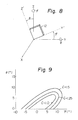
- Figure 8 shows an X-cut plate of double rotation, in which the plate is rotated about the Y-axis by angle 8 and about the Z-axis by angle ⁇ .
- the influence of temperature change upon the resonance frequency mainly depends upon the primary temperature coefficient of the resonance chip. If the temperature characteristic of the resonance chip is to be optimal, the primary temperature coefficient thereof should be zero.
- Figure 9 is a graphic view of the relationship between the orientation of the crystal and the trapped energy ⁇ , with respect to the strip shaped resonance chip of the double--rotation X-cut plate which has the primary temperature coefficient of zero.
- the trapped energy is defined as follows.
- the abscissa represents the ambient temperature ( O C) and the ordinate represents the shift of resonance frequency (ppm).
- the shift of resonance frequency is represented by Afr/fr, in which fr is the resonance frequency of the specimen (resonance chip) used in the experiment and ⁇ fr is the shifted amount of resonance frequency in response to the change of temperature.
- Each graph represents the temperature characteristic of different trapped energy ⁇ . The trapped energy is changed by changing the length l of the electrode.
- the X-cut plate used in the experiment was a 3° Y-X-cut plate rotated about the Y-axis by an angle 6 of 3°.
- the turning point is higher than 25°C when of the specimen is smaller than 1.06.
- the turning point is lower when ⁇ is increased.
- the abscissa represents the rotated angle of the resonance chip of the X-cut plate of lithium tantalate about the Y-axis of the crystal.
- the ordinate represents the trapped energy ⁇ .
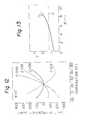
- Graph F Y represents the relationship between the angle 8 and the enclosed energy ⁇ , in which relationship the turning point of the temperature characteristic of the resonance chip is about normal room temperature (23°C).
- the dotted line G represents the maximum value of the trapped energy required for the single mode resonance of the strip shaped chip of lithium tantalate, experimentally examined at 3.6 MHz.
- Graph F Z in Fig. 13 represents the relationship between ⁇ and l for obtaining the temperature characteristic in which the apex temperature is equal to normal room temperature.
- the condition of single mode oscillation of the resonance chip of normal frequency is ⁇ ⁇ 1.25. Therefore, l/H ⁇ 3.95 is derived from the aforementioned formula (a).
- Graph F Z is below G when l is less than about 6°, i.e., the rotational angle about the Z-axis is within the range of -6° to 6°.
- Figure 14 is a graphic view of experimental results of the quality factor Q with respect to L/H, in which L is the length and H is the thickness of the resonance chip of lithium tantalate of Fig. 2.
- the abscissa represents L/H and the ordinate represents Q.
- the graph represents the relationship between Q and L/H.
- Q is constant in the region of L/H > 14 but falls in the region of L/H ⁇ 14. Therefore, it is desirable that L/H be larger than 14 so as to obtain resonance chips of stable and high quality.
- Figure 15 is a perspective view of the resonance chip of lithium tantalate of Fig. 2 for explaining the oscillation modes of the resonance chip.
- Figure 16 is a graphic view of the frequency characteristic of the resonance chip.
- Figure 17 is a graphic view of the admittance characteristic of the resonance chip.
- the abscissa represents frequency (MHz) and the ordinate represents response level (dB).
- the graph represents the frequency characteristic of the resonance chip.
- the peak P of the graph corresponds to the resonance of the thickness shear mode M.
- the peak P 2 is a spurious response which is generated when the width shear mode m interferes the thickness shear mode M. If the frequency of this spurious response is near that of the peak P 1 , the characteristic of the resonance chip is degraded.
- the abscissa represents the frequency f and the ordinate represents the admittance.
- the graph represents the admittance characteristic of the resonance chip.
- Point fr on the abscissa designates the frequency of the resonance and point fa designates the frequency of the antiresonance.
- the frequency of the resonance of the resonance chip is unstable if the spurious response is generated near the frequency point of fr. Therefore, the spurious responses must be sufficiently away from the point fr.
- Figure 18 is a graphic view of experimental results of the constant k (Hz ⁇ m) of frequency in which spurious response is generated due to the width shear mode, with respect to the ratio W/H.
- Fig. 18 the abscissa represents W/H and the ordinate represents k.
- Graphs D, E, and F represent the relationship between k and W/H with respect to the first, third, and fifth width shear mode, respectively, in which spurious responses are generated.
- the dotted line fr represents k of resonance.
- the dash-dot line fa represents antiresonance.
- the dash-two dot line represents the.minimum k for avoiding adverse influence from the spurious response.
- a first region G of W/H between about 1.35 and 3
- a second region G 2 of W/H between about 3.8 and 5 are free from adverse influence of spurious response.
- Figures 19 to 21 are views for explaining the construction of the resonance chip embodying the present invention.
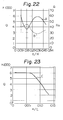
- Figure 22 is a graphic view of experimental results of the quality factor Q and the equivalence series resistance R S with respect to the thickness ratio t/H
- Figure 23 is a graphic view of another experimental result of the quality factor Q with respect to width ratio w/L.
- Figure 24 is a graphic view of the frequency characteristics of the resonance chip in which the thickness ratio t/H is 0.1.
- Figure 25 is a graphic view of the frequency characteristic of the resonance chip in which the thickness ratio t/H is 0.36.
- a strip shaped resonance chip plate 3' of lithium tantalate which has a rectangular cross-section is illustrated.
- the length and the thickness of the resonance chip plate 3' are represented by L and H, respectively.
- T shaped electrode patterns 4 and 4' are formed by an evaporation method on the upper and lower surfaces of the resonance chip plate 3'.
- two pairs of terminal conductors 13, 13' and 14, 14' are formed on both ends of the resonance chip plate 3' by a printing method.
- the terminal conductor 13 is superposed on the end of the electrode 4.
- the terminal conductor 14' is superposed on the end of the electrode 4'.
- each pair of terminal conductors 13, 13' and 14, 14' is connected by a connecting conductor 15 or 16, so as to form a resonance chip 3, as illustrated in Fig. 21.
- the terminal conductors 13, 13', 14, 14' are printed by using conductive paste such as silver paste.
- the thickness t and the width w of each terminal conductor are determined on the basis of experimental results, described later, so that the thickness ratio t/H is about 0.27 to 0.43 and the width ratio w/L is smaller than 0.06.
- the resonance chip 3 is mounted on a base (not shown) of a resonator package (not shown).
- a lead wire of the resonator package is connected to each of the electrode 4, 4' through the terminal conductors 13, 14' and the connecting conductors 15, 16.
- the connection between the lead wire and the connecting conductors 15, 16 is achieved simultaneously with the forming process of the connecting conductors 15, 16 by the printing method. Assembly of the resonator package is completed by covering the base by a cap (not shown).
- the abscissa represents the thickness ratio t/H of the terminal conductor.
- the ordinate of the left represents the quality factor Q.
- the ordinate of the right represents the equivalence series resistance R S .
- Graphs A and B represent the relationship between t/H and Q and the relationship between t/H and R s, respectively. Both graphs are based on experimental data.
- the resonance chip of lithium tantalate used in the experiment has a length L of 8 mm, a width W of 1.6 mm, a thickness H of 0.55 mm, and a width ratio w/L of 0.05.
- the value of Q is minimized when the thickness ratio t/H is 0.18, in which the value of Q is about 3,750.
- the desirable value of Q is larger than 5,000. Therefore, the thickness ratio t/H should be less than 0.11 or between 0.27 and 0.46.
- the resonance resistance R S is maximum (45 n) when the thickness ratio t/H is 0.18.
- the desirable value of R S is below 30 ⁇ . Therefore, the thickness ratio t/H should be 0.29 to 0.42.
- the desirable range of the thickness ratio t/H is between 0.29 and 0.42.
- the abscissa represents the width ratio w/L and the ordinate represents the quality coefficient Q.
- Graph C represents experimental results of the relationship between w/L and Q. As can be seen from Fig. 23, the value of Q is constant (about 6,000) when the width ratio w/L is below 0.06 and decreases when the width ratio w/L exceeds 0.06. Therefore, the width ratio w/L should be below 0.06 in order to obtain a desirable value of Q.
- the abscissa represents the frequency (MHz) and the ordinate represents the response level (dB).
- the graph represents the frequency characteristic of the resonance chip in which the thickness ratio t/H is 0.1, which is out of the aforementioned desirable range, i.e., between 0.29 to 0.42. As can be seen from this graph, spurious response is generated in the critical region of the frequency.
- the abscissa and the ordinate represent the same parameters as those of Fig. 24.
- the graph represents the frequency characteristic of the resonance chip in which the thickness ratio t/H is 0.36, which is within the aforementioned desirable range, i.e., between 0.29 and 0.42. Spurious oscillation is eliminated from the critical region of the frequency as was seen in Fig. 24.
- the angle between the longitudinal direction of a resonance chip embodying the present invention and the Y-axis of the crystal is determined to be -50 ⁇ 2° ; in this way efficiency of transformation'can be increased and spurious response . can be reduced, . with the result that the quality of the resonator is upgraded.
- An optimal temperature characteristic can be obtained without generating spurious response by selecting the trapped energy ⁇ in view of the angle rotated about each axis of the crystal.
- An optimal ratio of the thickness of the resonance chip to the length thereof and an optimal ratio of the width of the resonator chip to the thickness thereof can be determined, so that a resonator of high reliability and high quality in which spurious response is effectively eliminated can be obtained.
- an optimal dimension of the terminal conductor formed on each end of the resonance plate can be determined, so that it is possible to obtain a resonator of high reliability and high quality in which spurious response is effectively eliminated.
Landscapes
- Physics & Mathematics (AREA)
- Acoustics & Sound (AREA)
- Chemical & Material Sciences (AREA)
- Engineering & Computer Science (AREA)
- Ceramic Engineering (AREA)
- Piezo-Electric Or Mechanical Vibrators, Or Delay Or Filter Circuits (AREA)
Applications Claiming Priority (8)
| Application Number | Priority Date | Filing Date | Title |
|---|---|---|---|
| JP25993/82 | 1982-02-22 | ||
| JP2599382A JPS58143619A (ja) | 1982-02-22 | 1982-02-22 | 高結合圧電振動子 |
| JP65945/82 | 1982-04-20 | ||
| JP6594582A JPS58188915A (ja) | 1982-04-20 | 1982-04-20 | 圧電振動子 |
| JP7245082A JPS58190115A (ja) | 1982-04-28 | 1982-04-28 | 圧電振動子 |
| JP72450/82 | 1982-04-28 | ||
| JP11799982A JPS5910017A (ja) | 1982-07-07 | 1982-07-07 | LiTaO↓3圧電振動素子 |
| JP117999/82 | 1982-07-07 |
Publications (3)
| Publication Number | Publication Date |
|---|---|
| EP0088548A2 true EP0088548A2 (de) | 1983-09-14 |
| EP0088548A3 EP0088548A3 (en) | 1985-07-31 |
| EP0088548B1 EP0088548B1 (de) | 1988-06-08 |
Family
ID=27458412
Family Applications (1)
| Application Number | Title | Priority Date | Filing Date |
|---|---|---|---|
| EP83300872A Expired EP0088548B1 (de) | 1982-02-22 | 1983-02-18 | Piezoelektrische Resonatoren |
Country Status (3)
| Country | Link |
|---|---|
| US (1) | US4454444A (de) |
| EP (1) | EP0088548B1 (de) |
| DE (1) | DE3377043D1 (de) |
Families Citing this family (20)
| Publication number | Priority date | Publication date | Assignee | Title |
|---|---|---|---|---|
| US4583019A (en) * | 1983-05-30 | 1986-04-15 | Fujitsu Limited | Piezoelectric resonator using 165° Y-cut LiNbO3 |
| CA1281810C (en) * | 1984-02-20 | 1991-03-19 | Stephen P. Rogerson | Mounting of saw devices |
| JPH06123634A (ja) * | 1992-08-31 | 1994-05-06 | Murata Mfg Co Ltd | 振動ジャイロ |
| GB2277228B (en) * | 1993-04-14 | 1996-12-04 | Murata Manfacturing Co Ltd | Vibrator,resonator and resonance component utilizing width expansion mode |
| DE4419085C2 (de) * | 1993-05-31 | 1999-09-02 | Murata Manufacturing Co | Chipförmiger Baustein mit piezoelektrischer Resonanz |
| US5621263A (en) * | 1993-08-09 | 1997-04-15 | Murata Manufacturing Co., Ltd. | Piezoelectric resonance component |
| US5648746A (en) * | 1993-08-17 | 1997-07-15 | Murata Manufacturing Co., Ltd. | Stacked diezoelectric resonator ladder-type filter with at least one width expansion mode resonator |
| CN1064490C (zh) * | 1993-08-17 | 2001-04-11 | 株式会社村田制作所 | 梯形滤波器 |
| JP3114526B2 (ja) * | 1994-10-17 | 2000-12-04 | 株式会社村田製作所 | チップ型圧電共振部品 |
| US5572082A (en) * | 1994-11-14 | 1996-11-05 | Sokol; Thomas J. | Monolithic crystal strip filter |
| JP3218971B2 (ja) * | 1996-04-01 | 2001-10-15 | 株式会社村田製作所 | ラダー形フィルタ |
| US5998909A (en) * | 1996-05-15 | 1999-12-07 | Tokin Corporation | Piezoelectric transformer |
| JP3262007B2 (ja) * | 1997-01-10 | 2002-03-04 | 株式会社村田製作所 | エネルギー閉じ込め型厚みすべり共振子およびこの共振子を用いた電子部品 |
| JP3296264B2 (ja) * | 1997-09-11 | 2002-06-24 | 株式会社村田製作所 | 圧電部品 |
| US6621194B1 (en) | 1999-11-15 | 2003-09-16 | Matsushita Electric Industrial Co., Ltd. | Piezoelectric element having thickness shear vibration and mobile communication device using the same |
| EP1176716A3 (de) * | 2000-07-25 | 2003-11-26 | TDK Corporation | Piezoelektrischer Resonator, piezoelektrisches Resonatorbauteil und Verfahren zur Herstellung |
| JP2002246871A (ja) * | 2001-02-19 | 2002-08-30 | Matsushita Electric Ind Co Ltd | 圧電振動子、この圧電振動子を用いた梯子型フィルタおよび2重モード圧電フィルタ |
| TW201251157A (en) | 2011-06-03 | 2012-12-16 | Seiko Epson Corp | Piezoelectric vibration element, manufacturing method for piezoelectric vibration element, piezoelectric vibrator, electronic device, and electronic apparatus |
| CN102957394B (zh) * | 2011-08-18 | 2016-12-21 | 精工爱普生株式会社 | 振动元件、振子、电子装置、电子设备、移动体及振动元件的制造方法 |
| US8970316B2 (en) | 2011-08-19 | 2015-03-03 | Seiko Epson Corporation | Resonating element, resonator, electronic device, electronic apparatus, and mobile object |
Family Cites Families (3)
| Publication number | Priority date | Publication date | Assignee | Title |
|---|---|---|---|---|
| US3525885A (en) * | 1967-06-01 | 1970-08-25 | Bell Telephone Labor Inc | Low temperature-frequency coefficient lithium tantalate cuts and devices utilizing same |
| FR2235532A1 (en) * | 1973-06-29 | 1975-01-24 | Brunot Michel | Adjustable frequency piezo-electric filter - material resonance is obtained by exciting through range of impedance modes |
| JPS5468194A (en) * | 1977-11-11 | 1979-06-01 | Fujitsu Ltd | Thickness slippage vibrator |
-
1983
- 1983-02-18 DE DE8383300872T patent/DE3377043D1/de not_active Expired
- 1983-02-18 EP EP83300872A patent/EP0088548B1/de not_active Expired
- 1983-02-18 US US06/467,810 patent/US4454444A/en not_active Expired - Lifetime
Also Published As
| Publication number | Publication date |
|---|---|
| DE3377043D1 (en) | 1988-07-14 |
| US4454444A (en) | 1984-06-12 |
| EP0088548A3 (en) | 1985-07-31 |
| EP0088548B1 (de) | 1988-06-08 |
Similar Documents
| Publication | Publication Date | Title |
|---|---|---|
| EP0088548A2 (de) | Piezoelektrische Resonatoren | |
| US4418299A (en) | Face-shear mode quartz crystal vibrators and method of manufacture | |
| US4139793A (en) | Integral resonant support arms for piezoelectric microresonators | |
| US4633124A (en) | Mount for quartz crystal resonator | |
| JP2000514278A (ja) | 表面がマイクロ機械加工された音響波ピエゾ電気結晶 | |
| US6362561B1 (en) | Piezoelectric vibration device and piezoelectric resonance component | |
| US5311096A (en) | KT cut width-extensional mode quartz crystal resonator | |
| US5548180A (en) | Vibrator resonator and resonance component utilizing width expansion mode | |
| EP0127442B1 (de) | Piezoelektrischer Resonator | |
| JPH09275325A (ja) | 圧電共振子およびそれを用いた電子部品 | |
| CN1533030B (zh) | 压电振动片、压电振子及压电器件 | |
| JPH10154920A (ja) | ラダー型フィルタ | |
| EP0809356B1 (de) | Piezoelektrisches Bauelement | |
| JP3266031B2 (ja) | 圧電共振子およびそれを用いた電子部品 | |
| JP2001257558A (ja) | 圧電振動子 | |
| KR100280072B1 (ko) | 압전공진자및이를구비한전자부품 | |
| GB2125211A (en) | Mechanical support of piezoelectric devices | |
| US5487211A (en) | Method for fabricating a surface-mountable crystal resonator | |
| JP3363457B2 (ja) | 捩り水晶振動子 | |
| US5444325A (en) | Surface-mountable crystal resonator | |
| JPS59127413A (ja) | タンタル酸リチウム振動子 | |
| JPH04259109A (ja) | 2ポートsaw共振子 | |
| JP2854581B2 (ja) | 圧電振動素子とその周波数調整方法 | |
| US2259317A (en) | Piezoelectric crystal apparatus | |
| KR100330500B1 (ko) | 에너지 포획형 압전세라믹 공진장치 |
Legal Events
| Date | Code | Title | Description |
|---|---|---|---|
| PUAI | Public reference made under article 153(3) epc to a published international application that has entered the european phase |
Free format text: ORIGINAL CODE: 0009012 |
|
| AK | Designated contracting states |
Designated state(s): DE FR GB |
|
| PUAL | Search report despatched |
Free format text: ORIGINAL CODE: 0009013 |
|
| AK | Designated contracting states |
Designated state(s): DE FR GB |
|
| 17P | Request for examination filed |
Effective date: 19851002 |
|
| 17Q | First examination report despatched |
Effective date: 19861125 |
|
| GRAA | (expected) grant |
Free format text: ORIGINAL CODE: 0009210 |
|
| AK | Designated contracting states |
Kind code of ref document: B1 Designated state(s): DE FR GB |
|
| REF | Corresponds to: |
Ref document number: 3377043 Country of ref document: DE Date of ref document: 19880714 |
|
| ET | Fr: translation filed | ||
| PLBE | No opposition filed within time limit |
Free format text: ORIGINAL CODE: 0009261 |
|
| STAA | Information on the status of an ep patent application or granted ep patent |
Free format text: STATUS: NO OPPOSITION FILED WITHIN TIME LIMIT |
|
| 26N | No opposition filed | ||
| PGFP | Annual fee paid to national office [announced via postgrant information from national office to epo] |
Ref country code: FR Payment date: 19921229 Year of fee payment: 11 |
|
| PG25 | Lapsed in a contracting state [announced via postgrant information from national office to epo] |
Ref country code: FR Effective date: 19941031 |
|
| REG | Reference to a national code |
Ref country code: FR Ref legal event code: ST |
|
| PGFP | Annual fee paid to national office [announced via postgrant information from national office to epo] |
Ref country code: DE Payment date: 20010212 Year of fee payment: 19 |
|
| PGFP | Annual fee paid to national office [announced via postgrant information from national office to epo] |
Ref country code: GB Payment date: 20010214 Year of fee payment: 19 |
|
| REG | Reference to a national code |
Ref country code: GB Ref legal event code: IF02 |
|
| PG25 | Lapsed in a contracting state [announced via postgrant information from national office to epo] |
Ref country code: GB Free format text: LAPSE BECAUSE OF NON-PAYMENT OF DUE FEES Effective date: 20020218 |
|
| PG25 | Lapsed in a contracting state [announced via postgrant information from national office to epo] |
Ref country code: DE Free format text: LAPSE BECAUSE OF NON-PAYMENT OF DUE FEES Effective date: 20020903 |
|
| GBPC | Gb: european patent ceased through non-payment of renewal fee |
Effective date: 20020218 |