EP0089158A2 - Taktgesteuerter Spannungs-Frequenz-Wandler nach der Zweischrittmethode - Google Patents
Taktgesteuerter Spannungs-Frequenz-Wandler nach der Zweischrittmethode Download PDFInfo
- Publication number
- EP0089158A2 EP0089158A2 EP83301184A EP83301184A EP0089158A2 EP 0089158 A2 EP0089158 A2 EP 0089158A2 EP 83301184 A EP83301184 A EP 83301184A EP 83301184 A EP83301184 A EP 83301184A EP 0089158 A2 EP0089158 A2 EP 0089158A2
- Authority
- EP
- European Patent Office
- Prior art keywords
- output
- pulse
- pulses
- converter
- clock
- Prior art date
- Legal status (The legal status is an assumption and is not a legal conclusion. Google has not performed a legal analysis and makes no representation as to the accuracy of the status listed.)
- Granted
Links
- 230000009977 dual effect Effects 0.000 title claims abstract description 8
- 230000001360 synchronised effect Effects 0.000 claims abstract description 5
- 239000003990 capacitor Substances 0.000 claims description 13
- 230000000694 effects Effects 0.000 claims description 7
- 230000004044 response Effects 0.000 claims description 7
- 230000001419 dependent effect Effects 0.000 claims description 5
- 230000000977 initiatory effect Effects 0.000 claims description 4
- 238000007599 discharging Methods 0.000 claims description 2
- 230000001960 triggered effect Effects 0.000 abstract 1
- 238000010586 diagram Methods 0.000 description 15
- 230000004048 modification Effects 0.000 description 6
- 238000012986 modification Methods 0.000 description 6
- 230000007704 transition Effects 0.000 description 5
- 230000008859 change Effects 0.000 description 4
- 238000012935 Averaging Methods 0.000 description 3
- 230000008901 benefit Effects 0.000 description 3
- 238000000034 method Methods 0.000 description 2
- 230000000630 rising effect Effects 0.000 description 2
- 206010065929 Cardiovascular insufficiency Diseases 0.000 description 1
- 239000013078 crystal Substances 0.000 description 1
- 230000036039 immunity Effects 0.000 description 1
- 230000006872 improvement Effects 0.000 description 1
- 230000007246 mechanism Effects 0.000 description 1
- 230000000737 periodic effect Effects 0.000 description 1
- 230000008569 process Effects 0.000 description 1
- 238000011160 research Methods 0.000 description 1
- 238000012546 transfer Methods 0.000 description 1
Images


Classifications
-
- H—ELECTRICITY
- H03—ELECTRONIC CIRCUITRY
- H03K—PULSE TECHNIQUE
- H03K7/00—Modulating pulses with a continuously-variable modulating signal
- H03K7/06—Frequency or rate modulation, i.e. PFM or PRM
Definitions
- the present invention relates to clock controlled dual slope voltage to frequency converters.
- Various types oi voltage to frequency converters are known and a useful summary of the various kinds is published in "Designing With Operational Amplifiers - Application Alternatives", 1977, Burr-Brown Research Corporation, Chapter 8.2 (pages 212-223).
- the highest precision form of converter as discussed in the above publication is the clock controlled converter which uses a precision clock signal to determine the duration of the constant current discharge pulse applied to the integrator circuit to provide dual slope operation.
- the problem with such clock controlled converters is that the frequency output signal of the converter is always a subharmonic of the clock frequency, although the average of the output signal frequency is the desired output frequency.
- Such converters can have high precision, they have an inherent delay resulting from the need to average the frequency of the output signal.
- the present invention provides a converter which obtains the benefits of clock controlled operation whilst providing directly an output frequency which is not phase related to the clock frequency so that frequency averaging is not required.
- a clock controlled dual slope voltage to frequency converter comprising an input terminal for an input voltage to the converter, an integrator connected to said input terminal to provide an output signal having a charging slope dependent on said input voltage, a clock pulse source, comparator means arranged to provide an output indication in response to each occasion the output signal of the integrator exceeds a predetermined threshold level during charging, discharge pulse generating means arranged to supply, following said output indication, a constant current discharge pulse to the integrator having a constant pulse duration determined by clock pulses from the clock pulse source, whereby the output signal of the integrator has a discharging slope and falls below said predetermined threshold level during each said discharge pulse, frequency signal output means including at least one output terminal of the converter and connected to the output of the comparator.means to provide a frequency signal on the output terminal synchronised with the output indications of the comparator means, or a respective said synchronisedfrequency signal on each output terminal.
- an output frequency signal is generated which is not phase related to the clock fre- quen q r, but synchronised with the successive occasions on which the integrator charging slope exceeds the threshold level of the comparator. Between each such occasion, a constant current and duration discharge pulse is applied to the integrator to produce the discharge slope providing dual slope operation. It can be seen that, with a constant input voltage signal, the periods between successive such occasions providing an output indication from the comparator, are constant. Thus, the output frequency signal of the converter, has a constant frequency which is not phase related to the clock frequency. Nevertheless, the discharge pulses are accurately defined in duration by the clock pulses.
- the comparator means provides a pulse as each said output indication, and thus the frequency signal output means may include simply an electrical connection from the output of the comparator means to the output terminal, or one of the output terminals, so that said frequency signal on said terminal is constituted by the successive output pulses of the comparator means.
- the comparator means operates to initiate a pulse as each said output indication, i.e. the output state of the comparator means switches over as the integrator output exceeds the threshold.
- the duration of the pulses from the comparator means are not normally constant depending on the mechanism for switching the comparator means back again.
- the frequency signal output means includes a flip-flop clocked by said successive output pulses of the comparator means to switch between its output states in response to the initiations of said output pulses, the flip-flop having its output connected to the output terminal or one of the output terminals to provide said frequency signal on said output terminal.
- the frequency signal comprises a unity mark/space ratio wave form at a frequency equal to half the comparator output pulse rate.
- the frequency signal output means may include pulse stretching means to feed to the output terminal pulses initiated with the initiation of said pulses from the comparator means and having durations between a minimum of one clock period and a maximum of two clock periods.
- the comparator means comprises a Schmitt trigger circuit having a predetermined hysteresis between switching thresholds, one said threshold providing said predetermined threshold level.
- the converter may include a mode switch arranged to connect the integrator output signal to the Schmitt trigger circuit during each said charging slope and to connect a source of voltage beyond the other of said Schmitt thresholds to the Schmitt trigger circuit during each said discharge pulse to ensure return switching of the Schmitt trigger circuit ready for the next charging slope.
- the integrator may comprise an operational amplifier having the input voltage fed to its non-inverting input, a capacitor interconnecting the output of the amplifier and its inverting input, a resistor connected to the inverting input and a switch arranged to connect the resistor in series selectively to one of two different reference voltage sources, the discharge pulse generating means controlling the switch to connect the resistor alternately to one reference voltage source to effect the charging slope of the integrator output signal and to the other said source for said constant duration to provide each said discharge pulse.
- An operational amplifier can also be arranged to provide an inverting integrator by connecting the capacitor and resistor of the non-inverting arrangement described above instead to the inverting input of the amplifier, the non-inverting input then being connected to ground.
- the non-inverting arrangement of an operational amplifier integrator has the drawback that the output signal includes a term proportional to the input voltage signal. This may not be important for input voltages which are very small compared to the output swing of the integrator.
- said comparator means may be arranged to be responsive directly to the input voltage to the non-inverting input of the amplifier to cancel out the effect of the component of the integrator output signal which is proportional to the input voltage.
- the present invention also envisages a clock controlled frequency to voltage converter having an input terminal for an input frequency signal to the coverter comprising a train of pulses at said input frequency, a clock pulse source, control pulse generating means arranged to produce a control pulse of constant duration determined by clock pulses from the clock pulse source, following the first pulse of said input train since the preceding control pulse, and integrating means including a capacitor, a resistor and a switch controlled by the control pulses to switch the capacitor via the resistor alternately between a reference voltage and ground, whereby the voltage across the capacitor is the reference voltage proportioned in accordance with the mark/space ratio of said control pulses.
- each pulse of the input frequency signal produces a control pulse at a time and having a duration determined by the clock pulses.
- the maximum input frequency is equal to half the clock pulse frequency. With some arrangements of this frequency to voltage ccnverter, input frequencies in excess of the above maximum frequency may cause the output voltage across the capacitor to fall below the maximum voltage corresponding to an input frequency equal to half of the clock frequency. It can be seen that normally each said control pulse has a duration equal to a single pulse period of the clock pulses and the maximum rate of said control pulses is half the clock pulse rate. In order to ensure that the output voltage of the converter is constant for all input frequencies in excess of the maximum, said control pulse generating means may be arranged to produce a subsequent control pulse in response to one or more pulses of said input train received
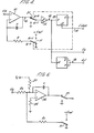
- an input voltage signal Vin is applied to the non-inverting input of an operational amplifier 10 connected as an integrator.
- a capacitor C is connected between the output of the amplifier 10 and the inverting input and a resistor R is connected from the inverting input to ground via a switch 11.
- the output signal V1 from the amplifier 10 comprises a positive going ramp having a slope proportional to Vin.
- the integrator output signal from the amplifier 10 is fed to a Schmitt trigger 12.
- the output signal from the Schmitt trigger switches to the "high” state as the integrator output exceeds the upper threshold voltage of the Schmitt.
- the Schmitt output V 2 is fed to the D input of a D-type flip-flop 13 which is clocked by a precision clock signal on a line 14.
- the D-type flip-flop 13 operates so that its Q output switches to a logic "1" on the first clock pulse after the signal on its D input goes high.
- the Q output of the flip-flop 13 is used to control the switch 11 to operate the switch to connect the resistor R to a source of reference voltage Vref so long as the Q output is at a logic "1".
- the output of the amplifier 10 ramps downwards with a downward slope dependent on the relative values of Vref and Vin.
- This dual slope operation of the integrator is established in the art.
- the Q output of the flip-flop 13 remains at a logic "1" until the immediately following clock pulse whereupon it reverts to a logic "O".
- the switch 11 is switched to the reference voltage for a precise period of time corresponding to one clock pulse period.
- the discharge pulse applied to the integrator to produce the down ramp has an accurately defined duration determined by the precision of the clock pulses supplied on line 14.
- FIG. 2 the sequential operation of the circuit as the output signal of the amplifier 10 repeatedly exceeds an upper threshold V H of the Schmitt trigger 12 is illustrated.
- the uppermost wave form in Figure 2 shows the output V 1 of the amplifier 10. During the positive going slope of the output, the charging slope, V 1 increases at the rate .
- Vref Vr
- the down slope of V 1 has a duration accurately defined as Thus the voltage drop of V 1 during each down slope is equal to
- the threshold crossings are accurately periodic and are not related in phase to the clock frequency f c .
- the third wave form shown in Figure 2 is the output signal V 2 of the Schmitt trigger 12.
- the output signal switches to a high state as V 1 exceeds the upper threshold V . of the Schmitt trigger and returns to a low state when V 1 crosses a lower switching threshold V L of the Schmitt during the downward slope.
- the hysteresis between V H and V L is normal for Schmitt trigger circuits and is useful in eliminating the jitter that can be experienced with an ordinary comparator resulting from noise on the ramp signal V 1 . Such jitter could produce errors by causing erroneous clocking of the flip-flop 13.
- the leading edges of the pulses produced by the Schmitt trigger 12 are at a frequency f 0 equal to f x .
- f is in no way phase related with the clock frequency f c .
- the output of the Schmitt trigger 12 is supplied, in the example of Figure 1, on a line 15 to an output terminal 16 for use as the frequency signal output of the converter.
- V 2 is supplied as the clock input to a toggle flip-flop 17 producing an output signal V 3 on a line 18 to a second output terminal 19.
- the wave form of V 3 is shown in Figure 2 and has a frequency f 0 ' equal to .
- V 3 has a unity mark/space ratio as illustrated.
- the output frequency f 0 ' can be counted over a period of time also determined by the clock frequency f , thereby giving a direct digital output in which any clock instability cancels out.
- VH is the maximum histeresis voltage of the Schmitt trigger between switching thresholds.
- Figure 3 is a timing diagram illustrating what happens if Vin exceeds the above limitation.
- the down ramp of V 1 does not reach the lower threshold V L in the time so that the D input to the flip-flop 13 is still high for the next clock pulse on line 14 causing the Q output of the flip-flop to remain at a logic "1".
- the down ramp of V 1 continues for a second clock period with the result that the period between successive transitions of V 1 with the upper threshold V H dc not remain constant.
- the hysteresis of the Schmitt trigger is desirable in providing some noise immunity as explained previously.
- one method of reducing the dynamic range limitation mentioned above is to minimise this hysteresis.
- the effect of the hysteresis band can be removed logically by a modification to the circuitry as illustrated in Figure 4.
- a mode change switch 21 is included between the output of the integrator 10 and the Schmitt trigger 12.
- the switch 21 is arranged to connect the output of the amplifier 10 to the Schmitt trigger 12 only when the Q output of the flip-flop 13 is at a logic "O", and to connect the input of the trigger 12 to ground when the Q output of the flip-flop 13 is at a logic "1".
- the effect of this modification is as illustrated in Figure 5 which shows that the Schmitt trigger 12 is forced to revert to a low output state as soon as the next clock pulse on line 14 toggles the flip-flop 13 causing the Q output to go to logic "1". This ensures that the Q output remains at a logic "1” only for one clock period even if the down ramp of the integrator output has not reached the lower switching threshold of the Schmitt 12.
- a further ranging improvement to the converter may be provided by implementing the integrator as an inverting summing integrator as illustrated in Figure 6.
- an amplifier 25 has its non-inverting input connected to ground via a resistor 26.
- the input voltage to the converter is supplied to the inverting input via a series resistor R s .
- Capacitor C is connected between the output of the amplifier and the inverting input and the inverting input is also connected via a series resistance R to the switch 11 which operates in the same manner as the circuits of Figures 1 and 4.
- the output of the amplifier 25 is supplied to a Schmitt trigger via a mode change switch 21 as before.
- Input voltage flexibility is thereby enhanced, albeit at the expense of two extra components in the circuit. Further the transfer equation of the converter is degraded by inaccuracies and temperature drift resulting from the factor . It should be noted also that the input signal must now be of opposite polarity.
- the circuit of Figure 6 can readily be modified to accommodate a bi-polarity input voltage range. Then, a further reference voltage V is connected to the inverting input via a further resistor 27 to provide a desired offset bias to the integrator.
- the non-inverting integrator arrangement is desirable in avoiding errors arising from temperature drift and inaccuracies in the resistors used for the inverting type integrator
- the non-inverting type has the disadvantage that its output signal includes a factor directly proportional to the input voltage.
- the output voltage of the non-inverting integrator is equal to In many cases, since the factor is much greater than 1, the influence of the Vin term in the output of the integrator is insignificant. However, when this is not the case, the effect of the term can be compensated for.
- Figures 7a and 7b illustrate two arrangements for compensating non-inverting integrators.
- the input voltage to the integrator is fed forward to a unity gain amplifier 30 connected as an analogue subtractor.
- the amplifier 30, subtracts Vin from the output of the integrator to produce a compensated output fed to the Schmitt trigger in the usual way.
- FIG. 7b there is illustrated an arrangement using a Schmitt trigger 31 which has an externally variable upper threshold.
- the input voltage to the integrator is fed forward to the Schmitt trigger 31 to control the upper threshold again to compensate for the Vin term in the integrator output.
- an output f 0 ' of the converter can have a unit mark/space ratio. However, in some arrangements, it may be necessary to employ the output f 0 in which the pulses are of varying duration. It may then be desirable to ensure that the pulses of the f o signal have a predetermined minimum duration, i.e. that the pulses are stretched if necessary.
- Figure 8 illustrates an appropriate circuit for stretching the pulses in the signal V 2 .
- the output of the Schmitt trigger V 2 is then supplied on a line 41 to the SET input of a flip-flop 40 so that the Q output of the flip-flop is set to a logic "1" as soon as the Schmitt output goes high.
- the flip-flop 40 is reset by a signal applied to its clock input on a line 42 from the Q output of the flip-flop 13, so that the Q output of the flip-flop 40 remains at a logic "1" until after the discharge pulse applied to the integrator amplifier 10 as determined by the flip-flop 13.
- the output pulses from the flip-flop 40 on line 43 supplied to an output terninal 14 have a minimum duration equal to and a maximum duration equal to
- Figure 9 illustrates a frequency to voltage converter which can resynchronise an unsynchronised input frequency signal f in with a local precision clock signal f c2 .
- Figure 10 shows a timing diagram illustrating the operation of this converter of Figure 9 at two different input frequencies f in .
- the pulse output signal from output Q 2 of a flip-flop 46 can be seen to have a duration and to occur once per .
- the limitation is that f in is not greater than This limit applies because it takes two clock periods to process each f in pulse.
- the averaging network including resistor capacitor RC and switch 47 produces an averaae output V 0 on terminal 48 equal to
- a mode change switch 49 interconnects the Q 1 output of flip-flop 45 to the D 2 input of flip-flop 46.
- the mode change switch 49 is arranged to connect Q 1 to D 2 when Q 2 is at a logic "O", and to connect D 2 to ground when Q 2 is a logic "1".
- flip-flop 46 is forced to toggle if the pulse rate on f in is high on each rising edge of the clock pulse f c2 .
- a further advantage of the frequency to voltage converter of Figure 9 is that a divider can be included in the clock line to flip-flop 46 effectively to provide digital gain.
- n is the divisor on f c2 .
Landscapes
- Manipulation Of Pulses (AREA)
Applications Claiming Priority (2)
| Application Number | Priority Date | Filing Date | Title |
|---|---|---|---|
| GB8207796 | 1982-03-17 | ||
| GB08207796A GB2118001B (en) | 1982-03-17 | 1982-03-17 | Clock controlled dual slope voltage to frequency converter |
Publications (3)
| Publication Number | Publication Date |
|---|---|
| EP0089158A2 true EP0089158A2 (de) | 1983-09-21 |
| EP0089158A3 EP0089158A3 (en) | 1984-09-19 |
| EP0089158B1 EP0089158B1 (de) | 1987-09-02 |
Family
ID=10529066
Family Applications (1)
| Application Number | Title | Priority Date | Filing Date |
|---|---|---|---|
| EP83301184A Expired EP0089158B1 (de) | 1982-03-17 | 1983-03-04 | Taktgesteuerter Spannungs-Frequenz-Wandler nach der Zweischrittmethode |
Country Status (4)
| Country | Link |
|---|---|
| US (1) | US4623800A (de) |
| EP (1) | EP0089158B1 (de) |
| DE (1) | DE3373395D1 (de) |
| GB (1) | GB2118001B (de) |
Cited By (1)
| Publication number | Priority date | Publication date | Assignee | Title |
|---|---|---|---|---|
| CN118694372A (zh) * | 2024-08-23 | 2024-09-24 | 中国科学院近代物理研究所 | 用于电离室探测器的模块化电流/频率转换装置及方法 |
Families Citing this family (8)
| Publication number | Priority date | Publication date | Assignee | Title |
|---|---|---|---|---|
| US4775841A (en) * | 1986-06-03 | 1988-10-04 | Trofimenkoff F N | Voltage to frequency conversion circuit with a pulse width to period ratio proportional to input voltage |
| US4866435A (en) * | 1987-10-16 | 1989-09-12 | Rosemount Inc. | Digital transmitter with variable resolution as a function of speed |
| US4827261A (en) * | 1987-11-04 | 1989-05-02 | Trofimenkoff Frederick N | Clock-controlled pulse width modulator |
| US4847620A (en) * | 1987-11-04 | 1989-07-11 | Trofimenkoff Frederick N | Clock-controlled voltage-to-frequency converter |
| US4992673A (en) * | 1989-02-24 | 1991-02-12 | John Fluke Mfg. Co., Inc. | Fast settling voltage to frequency converter for high speed analog to digital conversion |
| ATE133017T1 (de) * | 1990-04-19 | 1996-01-15 | Austria Mikrosysteme Int | Monolithisch integrierter hochauflösender analog- digital-umsetzer |
| US6064329A (en) * | 1996-07-02 | 2000-05-16 | Byrd; Eldon A. | System for creating and amplifying three dimensional sound employing phase distribution and duty cycle modulation of a high frequency digital signal |
| US6501399B1 (en) * | 1997-07-02 | 2002-12-31 | Eldon Byrd | System for creating and amplifying three dimensional sound employing phase distribution and duty cycle modulation of a high frequency digital signal |
Family Cites Families (11)
| Publication number | Priority date | Publication date | Assignee | Title |
|---|---|---|---|---|
| US3566283A (en) | 1968-08-19 | 1971-02-23 | Nus Corp | Signal converter |
| GB1312323A (en) * | 1970-09-22 | 1973-04-04 | Rosemount Eng Co Ltd | Signal processing circuits |
| US3778784A (en) | 1972-02-14 | 1973-12-11 | Intel Corp | Memory system incorporating a memory cell and timing means on a single semiconductor substrate |
| DE2212792B2 (de) | 1972-03-16 | 1975-02-13 | Siemens Ag, 1000 Berlin Und 8000 Muenchen | Spannungs-Frequenzwandler |
| US3749942A (en) | 1972-03-27 | 1973-07-31 | Lear Siegler Inc | Voltage to frequency converter for long term digital integration |
| US3778794A (en) * | 1972-09-18 | 1973-12-11 | Westinghouse Electric Corp | Analog to pulse rate converter |
| US3950989A (en) | 1974-07-30 | 1976-04-20 | Meirowitz Richard L | DC to frequency conversion circuit |
| US4031532A (en) * | 1975-12-29 | 1977-06-21 | First David J | Voltage to frequency converter |
| US4047056A (en) | 1976-11-02 | 1977-09-06 | Honeywell Inc. | Voltage-frequency converter |
| US4256983A (en) | 1979-05-02 | 1981-03-17 | General Electric Company | Voltage-to-frequency converter having a constant frequency mode of operation |
| DE2952156A1 (de) | 1979-12-22 | 1981-07-16 | Robert Bosch Gmbh, 7000 Stuttgart | Spannungs-frequenz-wandler, insbesondere fuer die verwendung in elektrischen steuersystemen von kraftfahrzeugen |
-
1982
- 1982-03-17 GB GB08207796A patent/GB2118001B/en not_active Expired
-
1983
- 1983-03-04 EP EP83301184A patent/EP0089158B1/de not_active Expired
- 1983-03-04 DE DE8383301184T patent/DE3373395D1/de not_active Expired
-
1985
- 1985-12-27 US US06/815,302 patent/US4623800A/en not_active Expired - Lifetime
Cited By (1)
| Publication number | Priority date | Publication date | Assignee | Title |
|---|---|---|---|---|
| CN118694372A (zh) * | 2024-08-23 | 2024-09-24 | 中国科学院近代物理研究所 | 用于电离室探测器的模块化电流/频率转换装置及方法 |
Also Published As
| Publication number | Publication date |
|---|---|
| DE3373395D1 (en) | 1987-10-08 |
| GB2118001A (en) | 1983-10-19 |
| GB2118001B (en) | 1986-03-12 |
| EP0089158B1 (de) | 1987-09-02 |
| US4623800A (en) | 1986-11-18 |
| EP0089158A3 (en) | 1984-09-19 |
Similar Documents
| Publication | Publication Date | Title |
|---|---|---|
| US4429236A (en) | Apparatus for generating pulses upon decreases in supply voltage | |
| US3535658A (en) | Frequency to analog converter | |
| EP0368398A1 (de) | Relaxationsoszillator mit Laufzeitsteuerung und verringerter Leistungsaufnahme | |
| EP0089158A2 (de) | Taktgesteuerter Spannungs-Frequenz-Wandler nach der Zweischrittmethode | |
| US4607238A (en) | Monolithic integrated RC-oscillator | |
| EP0525798B1 (de) | Integrierter Abtast-Halte-Phasendetektor mit einem stromeinstellenden integrierten Widerstand | |
| US4695742A (en) | Charge balance voltage-to-frequency converter utilizing CMOS circuitry | |
| US3277395A (en) | Pluse width modulator | |
| US5528186A (en) | Timing generator using digital signals to obtain accurate delay time and high resolution | |
| US4057796A (en) | Analog-digital converter | |
| US4775841A (en) | Voltage to frequency conversion circuit with a pulse width to period ratio proportional to input voltage | |
| US4672236A (en) | Voltage-to-frequency converter circuit | |
| US5051608A (en) | Circuit arrangement for supplying a periodic, substantially parabolic signal | |
| GB2047020A (en) | Reversible inverter system having control scheme | |
| SG54493G (en) | Analog-to-digital converter | |
| US4847620A (en) | Clock-controlled voltage-to-frequency converter | |
| CA1288138C (en) | Clock-controlled pulse width modulator | |
| US4507624A (en) | Voltage-to-frequency converters | |
| US4565992A (en) | Analog to digital converter | |
| EP0086334B1 (de) | Schaltung zur Änderung des Tastverhältnisses | |
| JP2513285B2 (ja) | サンプリングパルス発生回路 | |
| EP0128068A1 (de) | CMOS-Schaltung verwendender Spannungs-Frequenz-Wandler nach der Ladungsbilanzmethode | |
| JPS63219221A (ja) | クロツク周波数逓倍回路 | |
| SU1117610A1 (ru) | Источник стабилизированного напр жени | |
| SU474816A1 (ru) | Релейный операционный усилитель |
Legal Events
| Date | Code | Title | Description |
|---|---|---|---|
| PUAI | Public reference made under article 153(3) epc to a published international application that has entered the european phase |
Free format text: ORIGINAL CODE: 0009012 |
|
| AK | Designated contracting states |
Designated state(s): DE FR |
|
| PUAL | Search report despatched |
Free format text: ORIGINAL CODE: 0009013 |
|
| 17P | Request for examination filed |
Effective date: 19840618 |
|
| AK | Designated contracting states |
Designated state(s): DE FR |
|
| GRAA | (expected) grant |
Free format text: ORIGINAL CODE: 0009210 |
|
| AK | Designated contracting states |
Kind code of ref document: B1 Designated state(s): DE FR |
|
| REF | Corresponds to: |
Ref document number: 3373395 Country of ref document: DE Date of ref document: 19871008 |
|
| ET | Fr: translation filed | ||
| PLBE | No opposition filed within time limit |
Free format text: ORIGINAL CODE: 0009261 |
|
| STAA | Information on the status of an ep patent application or granted ep patent |
Free format text: STATUS: NO OPPOSITION FILED WITHIN TIME LIMIT |
|
| 26N | No opposition filed | ||
| PGFP | Annual fee paid to national office [announced via postgrant information from national office to epo] |
Ref country code: DE Payment date: 20020529 Year of fee payment: 20 |
|
| PGFP | Annual fee paid to national office [announced via postgrant information from national office to epo] |
Ref country code: FR Payment date: 20020604 Year of fee payment: 20 |