EP0089236A2 - Dispositif de commutation optique à membranes multiplanes - Google Patents
Dispositif de commutation optique à membranes multiplanes Download PDFInfo
- Publication number
- EP0089236A2 EP0089236A2 EP83301444A EP83301444A EP0089236A2 EP 0089236 A2 EP0089236 A2 EP 0089236A2 EP 83301444 A EP83301444 A EP 83301444A EP 83301444 A EP83301444 A EP 83301444A EP 0089236 A2 EP0089236 A2 EP 0089236A2
- Authority
- EP
- European Patent Office
- Prior art keywords
- channel
- light
- channels
- members
- plastic member
- Prior art date
- Legal status (The legal status is an assumption and is not a legal conclusion. Google has not performed a legal analysis and makes no representation as to the accuracy of the status listed.)
- Granted
Links
Images
Classifications
-
- G—PHYSICS
- G02—OPTICS
- G02B—OPTICAL ELEMENTS, SYSTEMS OR APPARATUS
- G02B6/00—Light guides; Structural details of arrangements comprising light guides and other optical elements, e.g. couplings
- G02B6/24—Coupling light guides
- G02B6/26—Optical coupling means
- G02B6/35—Optical coupling means having switching means
- G02B6/3536—Optical coupling means having switching means involving evanescent coupling variation, e.g. by a moving element such as a membrane which changes the effective refractive index
-
- G—PHYSICS
- G02—OPTICS
- G02B—OPTICAL ELEMENTS, SYSTEMS OR APPARATUS
- G02B6/00—Light guides; Structural details of arrangements comprising light guides and other optical elements, e.g. couplings
- G02B6/24—Coupling light guides
- G02B6/26—Optical coupling means
- G02B6/28—Optical coupling means having data bus means, i.e. plural waveguides interconnected and providing an inherently bidirectional system by mixing and splitting signals
- G02B6/2804—Optical coupling means having data bus means, i.e. plural waveguides interconnected and providing an inherently bidirectional system by mixing and splitting signals forming multipart couplers without wavelength selective elements, e.g. "T" couplers, star couplers
- G02B6/2852—Optical coupling means having data bus means, i.e. plural waveguides interconnected and providing an inherently bidirectional system by mixing and splitting signals forming multipart couplers without wavelength selective elements, e.g. "T" couplers, star couplers using tapping light guides arranged sidewardly, e.g. in a non-parallel relationship with respect to the bus light guides (light extraction or launching through cladding, with or without surface discontinuities, bent structures)
-
- G—PHYSICS
- G02—OPTICS
- G02B—OPTICAL ELEMENTS, SYSTEMS OR APPARATUS
- G02B6/00—Light guides; Structural details of arrangements comprising light guides and other optical elements, e.g. couplings
- G02B6/24—Coupling light guides
- G02B6/26—Optical coupling means
- G02B6/35—Optical coupling means having switching means
- G02B6/354—Switching arrangements, i.e. number of input/output ports and interconnection types
- G02B6/3544—2D constellations, i.e. with switching elements and switched beams located in a plane
- G02B6/3546—NxM switch, i.e. a regular array of switches elements of matrix type constellation
-
- G—PHYSICS
- G02—OPTICS
- G02B—OPTICAL ELEMENTS, SYSTEMS OR APPARATUS
- G02B6/00—Light guides; Structural details of arrangements comprising light guides and other optical elements, e.g. couplings
- G02B6/24—Coupling light guides
- G02B6/26—Optical coupling means
- G02B6/35—Optical coupling means having switching means
- G02B6/3564—Mechanical details of the actuation mechanism associated with the moving element or mounting mechanism details
- G02B6/3568—Mechanical details of the actuation mechanism associated with the moving element or mounting mechanism details characterised by the actuating force
- G02B6/3574—Mechanical force, e.g. pressure variations
Definitions
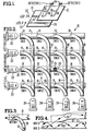
- the present invention relates to photo-optical switching devices and more specifically to multiplane optical membrane switches for use in keyboard matrix arrays.
- Prior art electrical membrane switching apparatus generally utilizes an electrically conductive coating on the opposite confronting surfaces of two slightly separated membranes. When the two membranes are pressed together electrical contact is made between the two conducting surfaces. If the conductive coatings are arranged in an array or matrix with one set of conductors at right angles to the other opposite set of conductors it is possible to form a keyboard with keys disposed at the intersections thereof.
- Such keyboards suffer from certain deficiences not the least of which is the fact that they radiate electromagnetic energy and are susceptible to electromagnetic interference (EMI).
- EMI electromagnetic interference
- the present invention provides an optically conductive keyboard membrane switch mechanism for use for example in keyboard applications among others.
- Two vertically displaced and separated planar, flat, sheet like membranes are each provided with a plurality of light conducting channels on one surface thereof.
- the channels of the upper membrane member are arranged to overlay the channels of the lower membrane member.
- the lower membrane may have horizontal or x row channels thereon while the upper membrane may have vertical or y column channels thereon.
- the upper planar channel carrying members also include individual taps or optically conductive tails that intersect or overlap the optical channels of the lower membrane.
- An optical switch structure is formed by placing a vertically movable key pad or key top over each tap such that depression of a key causes the upper channel intersecting area to contact the lower channel intersecting area.
- a light source is disposed at the entering portion or end of each horizontal x row light conducting lower channel member while a light detector is located at the light exiting portion or end of each vertically column upper light conductor or channel member.
- a light detector is located at the light exiting portion or end of each vertically column upper light conductor or channel member.
- Lexan a clear plastic manufactured by General Electric Corporation of New York, USA exhibits such properties and has been successfully employed in the subject invention. Lexan is the trademark of the General Electric Company.
- a matrix array of this material comprises a first horizontal x row of fiber optical channels or light guides 14 disposed on the lower sheet 10 with a second vertical column set of light guides 16 disposed on the upper sheet 12 at right angles to the guides 14.
- Light generating means 22 such as light emitting diodes ( L EDs) are located at each horizontal row input end as in Figure 1.
- Light detectors or receptors 24, such as phototransistors or photo diodes are disposed at the end of each vertical column. Depression of any key 20 in a row 12 will cause light 26 from the photo generator 22 to couple up into the selected column guide 16 and activate its respective light receptor 24.
- This invention provides a relatively inexpensive keyboard array of easily formed optical switch devices. For practical purposes no moving parts are employed and in fact nothing moves but the upper plane intersecting point as it contacts the lower plane intersecting point. Effectively reducing the number of parts required in the device as well as the fabrication time for assembly thereof.
Landscapes
- Physics & Mathematics (AREA)
- General Physics & Mathematics (AREA)
- Optics & Photonics (AREA)
- Push-Button Switches (AREA)
- Optical Elements Other Than Lenses (AREA)
- Switches Operated By Changes In Physical Conditions (AREA)
- Mechanical Light Control Or Optical Switches (AREA)
Applications Claiming Priority (2)
| Application Number | Priority Date | Filing Date | Title |
|---|---|---|---|
| US358823 | 1982-03-16 | ||
| US06/358,823 US4480183A (en) | 1982-03-16 | 1982-03-16 | Multi-plane optical membrane switch apparatus |
Publications (3)
| Publication Number | Publication Date |
|---|---|
| EP0089236A2 true EP0089236A2 (fr) | 1983-09-21 |
| EP0089236A3 EP0089236A3 (en) | 1986-07-16 |
| EP0089236B1 EP0089236B1 (fr) | 1988-11-09 |
Family
ID=23411192
Family Applications (1)
| Application Number | Title | Priority Date | Filing Date |
|---|---|---|---|
| EP83301444A Expired EP0089236B1 (fr) | 1982-03-16 | 1983-03-16 | Dispositif de commutation optique à membranes multiplanes |
Country Status (6)
| Country | Link |
|---|---|
| US (1) | US4480183A (fr) |
| EP (1) | EP0089236B1 (fr) |
| JP (1) | JPS59500433A (fr) |
| CA (1) | CA1209832A (fr) |
| DE (1) | DE3378431D1 (fr) |
| WO (1) | WO1983003311A1 (fr) |
Cited By (1)
| Publication number | Priority date | Publication date | Assignee | Title |
|---|---|---|---|---|
| CN101846772A (zh) * | 2009-03-23 | 2010-09-29 | 陈�峰 | 薄膜光波导纵横开关模块 |
Families Citing this family (14)
| Publication number | Priority date | Publication date | Assignee | Title |
|---|---|---|---|---|
| US4713535A (en) * | 1985-09-04 | 1987-12-15 | Rhoades Randy L | Optical keyboard |
| US4709141A (en) * | 1986-01-09 | 1987-11-24 | Rockwell International Corporation | Non-destructive testing of cooled detector arrays |
| US4733068A (en) * | 1986-04-07 | 1988-03-22 | Rockwell International Corporation | Crossed fiber optic tactile sensor |
| DE3865665D1 (de) * | 1988-02-17 | 1991-11-21 | Wolfgang Brunner | Messverfahren zum ortsaufgeloesten messen von druecken. |
| GB9119092D0 (en) * | 1991-09-06 | 1991-10-23 | Sarnoff David Res Center | Optomechanical keyboard |
| US5347123A (en) * | 1993-05-06 | 1994-09-13 | Motorola, Inc. | Optical control switch device having a plurality of light receptors |
| DE4422414A1 (de) * | 1994-06-29 | 1996-01-04 | Bfi Entsorgungstech | Optische Überwachungsanordnung |
| US5541405A (en) * | 1994-07-27 | 1996-07-30 | Parker-Hannifin Corporation | Method and device for continuous pattern sensing using fiber optics |
| US6097025A (en) * | 1997-10-31 | 2000-08-01 | Ljl Biosystems, Inc. | Light detection device having an optical-path switching mechanism |
| US6396070B1 (en) * | 1997-11-24 | 2002-05-28 | Datamax Corporation | Adjustable sensor assembly for printers |
| JP2004520661A (ja) * | 2001-05-23 | 2004-07-08 | コーニンクレッカ フィリップス エレクトロニクス エヌ ヴィ | センサ及び表示装置並びに記録装置 |
| US6654674B2 (en) * | 2001-11-21 | 2003-11-25 | Ford Global Technologies, Llc | Enhanced system for yaw stability control system to include roll stability control function |
| JP4284650B2 (ja) * | 2003-09-18 | 2009-06-24 | ヤマハ株式会社 | 光学検出装置 |
| US9344085B2 (en) * | 2013-03-27 | 2016-05-17 | Blackberry Limited | Keypad with optical sensors |
Family Cites Families (5)
| Publication number | Priority date | Publication date | Assignee | Title |
|---|---|---|---|---|
| US3982123A (en) * | 1974-11-11 | 1976-09-21 | Bell Telephone Laboratories, Incorporated | Optical fiber power taps |
| US4013342A (en) * | 1975-12-19 | 1977-03-22 | Narodny Leo H | Keyboard using optical switching |
| DE3010971A1 (de) * | 1980-03-21 | 1981-10-08 | Siemens AG, 1000 Berlin und 8000 München | Verfahren zur herstellung eines optischen 4-tor-kopplers |
| US4360247A (en) * | 1981-01-19 | 1982-11-23 | Gould Inc. | Evanescent fiber optic pressure sensor apparatus |
| JPS5875103A (ja) * | 1981-10-29 | 1983-05-06 | Matsushita Electric Works Ltd | 光スイツチ |
-
1982
- 1982-03-16 US US06/358,823 patent/US4480183A/en not_active Expired - Fee Related
-
1983
- 1983-03-15 WO PCT/US1983/000341 patent/WO1983003311A1/fr not_active Ceased
- 1983-03-15 JP JP58501350A patent/JPS59500433A/ja active Granted
- 1983-03-15 CA CA000423646A patent/CA1209832A/fr not_active Expired
- 1983-03-16 EP EP83301444A patent/EP0089236B1/fr not_active Expired
- 1983-03-16 DE DE8383301444T patent/DE3378431D1/de not_active Expired
Cited By (1)
| Publication number | Priority date | Publication date | Assignee | Title |
|---|---|---|---|---|
| CN101846772A (zh) * | 2009-03-23 | 2010-09-29 | 陈�峰 | 薄膜光波导纵横开关模块 |
Also Published As
| Publication number | Publication date |
|---|---|
| DE3378431D1 (en) | 1988-12-15 |
| JPH0548442B2 (fr) | 1993-07-21 |
| US4480183A (en) | 1984-10-30 |
| EP0089236B1 (fr) | 1988-11-09 |
| CA1209832A (fr) | 1986-08-19 |
| WO1983003311A1 (fr) | 1983-09-29 |
| JPS59500433A (ja) | 1984-03-15 |
| EP0089236A3 (en) | 1986-07-16 |
Similar Documents
| Publication | Publication Date | Title |
|---|---|---|
| US4480183A (en) | Multi-plane optical membrane switch apparatus | |
| EP0089237B1 (fr) | Commutateur optique plan à membrane et clavier l'utilisant | |
| EP0001000B1 (fr) | Commutateur optique | |
| US4580873A (en) | Optical matrix switch | |
| CA2283169C (fr) | Dispositif d'entree utilisateur pour systeme informatique | |
| KR930018928A (ko) | 완전밀착형 이미지센서 및 그 제조방법 | |
| US5220628A (en) | Circuit board assembly | |
| US20030202732A1 (en) | Optical switching apparatus with divergence correction | |
| EP0089235B1 (fr) | Dispositif moulé de commutation à guide d'onde | |
| CN103370650A (zh) | 波导型光开关 | |
| US6865310B2 (en) | Multi-layer thin film optical waveguide switch | |
| US4736190A (en) | Sheet membrane keyboard and electronic apparatus using same | |
| US7233715B2 (en) | Optical switch and optical switch system | |
| US6396972B1 (en) | Thermally actuated optical add/drop switch | |
| US7095913B2 (en) | Non-active waveguides on planar lightwave circuits | |
| JP2705853B2 (ja) | ラックに挿入可能な装置用の光信号接続装置 | |
| US7016561B2 (en) | Optical switch device having movable switching member | |
| EP0089238B1 (fr) | Clavier optique moulé avec des touches à fibres optiques | |
| JPS5915423B2 (ja) | マザ−ボ−ド及びパツケ−ジ間光接続方式 | |
| WO1983003314A1 (fr) | Clavier et commutateur a fibres enroulees | |
| US4976505A (en) | Optical switch using directionally flexible optical fibres | |
| GB1566654A (en) | Switches | |
| JPH0316005B2 (fr) | ||
| JPH06332022A (ja) | 光スイッチ素子を具えた光接続装置 | |
| EP1795926A1 (fr) | Module de fibres optiques, son procédé de fabrication et terminal nomade |
Legal Events
| Date | Code | Title | Description |
|---|---|---|---|
| PUAI | Public reference made under article 153(3) epc to a published international application that has entered the european phase |
Free format text: ORIGINAL CODE: 0009012 |
|
| 17P | Request for examination filed |
Effective date: 19830319 |
|
| AK | Designated contracting states |
Designated state(s): BE DE FR GB NL SE |
|
| PUAL | Search report despatched |
Free format text: ORIGINAL CODE: 0009013 |
|
| AK | Designated contracting states |
Kind code of ref document: A3 Designated state(s): BE DE FR GB NL SE |
|
| RAP1 | Party data changed (applicant data changed or rights of an application transferred) |
Owner name: BURROUGHS CORPORATION (A DELAWARE CORPORATION) |
|
| RAP1 | Party data changed (applicant data changed or rights of an application transferred) |
Owner name: UNISYS CORPORATION |
|
| 17Q | First examination report despatched |
Effective date: 19870812 |
|
| GRAA | (expected) grant |
Free format text: ORIGINAL CODE: 0009210 |
|
| AK | Designated contracting states |
Kind code of ref document: B1 Designated state(s): BE DE FR GB NL SE |
|
| REF | Corresponds to: |
Ref document number: 3378431 Country of ref document: DE Date of ref document: 19881215 |
|
| ET | Fr: translation filed | ||
| PLBE | No opposition filed within time limit |
Free format text: ORIGINAL CODE: 0009261 |
|
| STAA | Information on the status of an ep patent application or granted ep patent |
Free format text: STATUS: NO OPPOSITION FILED WITHIN TIME LIMIT |
|
| 26N | No opposition filed | ||
| PGFP | Annual fee paid to national office [announced via postgrant information from national office to epo] |
Ref country code: SE Payment date: 19920221 Year of fee payment: 10 |
|
| PGFP | Annual fee paid to national office [announced via postgrant information from national office to epo] |
Ref country code: BE Payment date: 19920409 Year of fee payment: 10 |
|
| PGFP | Annual fee paid to national office [announced via postgrant information from national office to epo] |
Ref country code: FR Payment date: 19921216 Year of fee payment: 11 |
|
| PG25 | Lapsed in a contracting state [announced via postgrant information from national office to epo] |
Ref country code: SE Effective date: 19930317 |
|
| PG25 | Lapsed in a contracting state [announced via postgrant information from national office to epo] |
Ref country code: BE Effective date: 19930331 |
|
| BERE | Be: lapsed |
Owner name: UNISYS CORP. Effective date: 19930331 |
|
| PGFP | Annual fee paid to national office [announced via postgrant information from national office to epo] |
Ref country code: DE Payment date: 19940329 Year of fee payment: 12 |
|
| PGFP | Annual fee paid to national office [announced via postgrant information from national office to epo] |
Ref country code: NL Payment date: 19940331 Year of fee payment: 12 |
|
| PG25 | Lapsed in a contracting state [announced via postgrant information from national office to epo] |
Ref country code: FR Effective date: 19941130 |
|
| REG | Reference to a national code |
Ref country code: FR Ref legal event code: ST |
|
| EUG | Se: european patent has lapsed |
Ref document number: 83301444.2 Effective date: 19931008 |
|
| PG25 | Lapsed in a contracting state [announced via postgrant information from national office to epo] |
Ref country code: NL Effective date: 19951001 |
|
| NLV4 | Nl: lapsed or anulled due to non-payment of the annual fee |
Effective date: 19951001 |
|
| PG25 | Lapsed in a contracting state [announced via postgrant information from national office to epo] |
Ref country code: DE Effective date: 19951201 |
|
| PGFP | Annual fee paid to national office [announced via postgrant information from national office to epo] |
Ref country code: GB Payment date: 19960208 Year of fee payment: 14 |
|
| PG25 | Lapsed in a contracting state [announced via postgrant information from national office to epo] |
Ref country code: GB Effective date: 19970316 |
|
| GBPC | Gb: european patent ceased through non-payment of renewal fee |
Effective date: 19970316 |