EP0089604A1 - Procédé pour le revêtement sélectif des échantillons métallurgiques se trouvant sur substrats diélectriques - Google Patents
Procédé pour le revêtement sélectif des échantillons métallurgiques se trouvant sur substrats diélectriques Download PDFInfo
- Publication number
- EP0089604A1 EP0089604A1 EP83102539A EP83102539A EP0089604A1 EP 0089604 A1 EP0089604 A1 EP 0089604A1 EP 83102539 A EP83102539 A EP 83102539A EP 83102539 A EP83102539 A EP 83102539A EP 0089604 A1 EP0089604 A1 EP 0089604A1
- Authority
- EP
- European Patent Office
- Prior art keywords
- substrate
- pattern
- metals
- metal
- alloy
- Prior art date
- Legal status (The legal status is an assumption and is not a legal conclusion. Google has not performed a legal analysis and makes no representation as to the accuracy of the status listed.)
- Granted
Links
Images


Classifications
-
- C—CHEMISTRY; METALLURGY
- C04—CEMENTS; CONCRETE; ARTIFICIAL STONE; CERAMICS; REFRACTORIES
- C04B—LIME, MAGNESIA; SLAG; CEMENTS; COMPOSITIONS THEREOF, e.g. MORTARS, CONCRETE OR LIKE BUILDING MATERIALS; ARTIFICIAL STONE; CERAMICS; REFRACTORIES; TREATMENT OF NATURAL STONE
- C04B41/00—After-treatment of mortars, concrete, artificial stone or ceramics; Treatment of natural stone
- C04B41/80—After-treatment of mortars, concrete, artificial stone or ceramics; Treatment of natural stone of only ceramics
- C04B41/81—Coating or impregnation
- C04B41/85—Coating or impregnation with inorganic materials
- C04B41/88—Metals
-
- B—PERFORMING OPERATIONS; TRANSPORTING
- B23—MACHINE TOOLS; METAL-WORKING NOT OTHERWISE PROVIDED FOR
- B23K—SOLDERING OR UNSOLDERING; WELDING; CLADDING OR PLATING BY SOLDERING OR WELDING; CUTTING BY APPLYING HEAT LOCALLY, e.g. FLAME CUTTING; WORKING BY LASER BEAM
- B23K35/00—Rods, electrodes, materials, or media, for use in soldering, welding, or cutting
- B23K35/001—Interlayers, transition pieces for metallurgical bonding of workpieces
-
- C—CHEMISTRY; METALLURGY
- C04—CEMENTS; CONCRETE; ARTIFICIAL STONE; CERAMICS; REFRACTORIES
- C04B—LIME, MAGNESIA; SLAG; CEMENTS; COMPOSITIONS THEREOF, e.g. MORTARS, CONCRETE OR LIKE BUILDING MATERIALS; ARTIFICIAL STONE; CERAMICS; REFRACTORIES; TREATMENT OF NATURAL STONE
- C04B41/00—After-treatment of mortars, concrete, artificial stone or ceramics; Treatment of natural stone
- C04B41/009—After-treatment of mortars, concrete, artificial stone or ceramics; Treatment of natural stone characterised by the material treated
-
- C—CHEMISTRY; METALLURGY
- C04—CEMENTS; CONCRETE; ARTIFICIAL STONE; CERAMICS; REFRACTORIES
- C04B—LIME, MAGNESIA; SLAG; CEMENTS; COMPOSITIONS THEREOF, e.g. MORTARS, CONCRETE OR LIKE BUILDING MATERIALS; ARTIFICIAL STONE; CERAMICS; REFRACTORIES; TREATMENT OF NATURAL STONE
- C04B41/00—After-treatment of mortars, concrete, artificial stone or ceramics; Treatment of natural stone
- C04B41/45—Coating or impregnating, e.g. injection in masonry, partial coating of green or fired ceramics, organic coating compositions for adhering together two concrete elements
- C04B41/50—Coating or impregnating, e.g. injection in masonry, partial coating of green or fired ceramics, organic coating compositions for adhering together two concrete elements with inorganic materials
- C04B41/51—Metallising, e.g. infiltration of sintered ceramic preforms with molten metal
-
- H—ELECTRICITY
- H05—ELECTRIC TECHNIQUES NOT OTHERWISE PROVIDED FOR
- H05K—PRINTED CIRCUITS; CASINGS OR CONSTRUCTIONAL DETAILS OF ELECTRIC APPARATUS; MANUFACTURE OF ASSEMBLAGES OF ELECTRICAL COMPONENTS
- H05K3/00—Apparatus or processes for manufacturing printed circuits
- H05K3/22—Secondary treatment of printed circuits
- H05K3/24—Reinforcing of the conductive pattern
- H05K3/245—Reinforcing conductive patterns made by printing techniques or by other techniques for applying conductive pastes, inks or powders; Reinforcing other conductive patterns by such techniques
- H05K3/246—Reinforcing conductive paste, ink or powder patterns by other methods, e.g. by plating
-
- H—ELECTRICITY
- H10—SEMICONDUCTOR DEVICES; ELECTRIC SOLID-STATE DEVICES NOT OTHERWISE PROVIDED FOR
- H10W—GENERIC PACKAGES, INTERCONNECTIONS, CONNECTORS OR OTHER CONSTRUCTIONAL DETAILS OF DEVICES COVERED BY CLASS H10
- H10W20/00—Interconnections in chips, wafers or substrates
- H10W20/01—Manufacture or treatment
- H10W20/031—Manufacture or treatment of conductive parts of the interconnections
- H10W20/056—Manufacture or treatment of conductive parts of the interconnections by filling conductive material into holes, grooves or trenches
- H10W20/057—Manufacture or treatment of conductive parts of the interconnections by filling conductive material into holes, grooves or trenches by selectively depositing, e.g. by using selective CVD or plating
-
- H—ELECTRICITY
- H10—SEMICONDUCTOR DEVICES; ELECTRIC SOLID-STATE DEVICES NOT OTHERWISE PROVIDED FOR
- H10W—GENERIC PACKAGES, INTERCONNECTIONS, CONNECTORS OR OTHER CONSTRUCTIONAL DETAILS OF DEVICES COVERED BY CLASS H10
- H10W70/00—Package substrates; Interposers; Redistribution layers [RDL]
- H10W70/01—Manufacture or treatment
- H10W70/05—Manufacture or treatment of insulating or insulated package substrates, or of interposers, or of redistribution layers
-
- H—ELECTRICITY
- H05—ELECTRIC TECHNIQUES NOT OTHERWISE PROVIDED FOR
- H05K—PRINTED CIRCUITS; CASINGS OR CONSTRUCTIONAL DETAILS OF ELECTRIC APPARATUS; MANUFACTURE OF ASSEMBLAGES OF ELECTRICAL COMPONENTS
- H05K1/00—Printed circuits
- H05K1/02—Details
- H05K1/03—Use of materials for the substrate
- H05K1/0306—Inorganic insulating substrates, e.g. ceramic, glass
-
- H—ELECTRICITY
- H05—ELECTRIC TECHNIQUES NOT OTHERWISE PROVIDED FOR
- H05K—PRINTED CIRCUITS; CASINGS OR CONSTRUCTIONAL DETAILS OF ELECTRIC APPARATUS; MANUFACTURE OF ASSEMBLAGES OF ELECTRICAL COMPONENTS
- H05K3/00—Apparatus or processes for manufacturing printed circuits
- H05K3/02—Apparatus or processes for manufacturing printed circuits in which the conductive material is applied to the surface of the insulating support and is thereafter removed from such areas of the surface which are not intended for current conducting or shielding
- H05K3/04—Apparatus or processes for manufacturing printed circuits in which the conductive material is applied to the surface of the insulating support and is thereafter removed from such areas of the surface which are not intended for current conducting or shielding the conductive material being removed mechanically, e.g. by punching
- H05K3/046—Apparatus or processes for manufacturing printed circuits in which the conductive material is applied to the surface of the insulating support and is thereafter removed from such areas of the surface which are not intended for current conducting or shielding the conductive material being removed mechanically, e.g. by punching by selective transfer or selective detachment of a conductive layer
- H05K3/048—Apparatus or processes for manufacturing printed circuits in which the conductive material is applied to the surface of the insulating support and is thereafter removed from such areas of the surface which are not intended for current conducting or shielding the conductive material being removed mechanically, e.g. by punching by selective transfer or selective detachment of a conductive layer using a lift-off resist pattern or a release layer pattern
-
- H—ELECTRICITY
- H05—ELECTRIC TECHNIQUES NOT OTHERWISE PROVIDED FOR
- H05K—PRINTED CIRCUITS; CASINGS OR CONSTRUCTIONAL DETAILS OF ELECTRIC APPARATUS; MANUFACTURE OF ASSEMBLAGES OF ELECTRICAL COMPONENTS
- H05K3/00—Apparatus or processes for manufacturing printed circuits
- H05K3/10—Apparatus or processes for manufacturing printed circuits in which conductive material is applied to the insulating support in such a manner as to form the desired conductive pattern
- H05K3/14—Apparatus or processes for manufacturing printed circuits in which conductive material is applied to the insulating support in such a manner as to form the desired conductive pattern using spraying techniques to apply the conductive material, e.g. vapour evaporation
- H05K3/143—Masks therefor
-
- H—ELECTRICITY
- H05—ELECTRIC TECHNIQUES NOT OTHERWISE PROVIDED FOR
- H05K—PRINTED CIRCUITS; CASINGS OR CONSTRUCTIONAL DETAILS OF ELECTRIC APPARATUS; MANUFACTURE OF ASSEMBLAGES OF ELECTRICAL COMPONENTS
- H05K3/00—Apparatus or processes for manufacturing printed circuits
- H05K3/22—Secondary treatment of printed circuits
- H05K3/24—Reinforcing of the conductive pattern
- H05K3/244—Finish plating of conductors, especially of copper conductors, e.g. for pads or lands
Definitions
- the invention relates to a method for selectively depositing layers of metals over an existing metallurgical pattern supported on a dielectric substrate.
- MLC multi-layer ceramic
- the punched and printed green sheets are selectively stacked on each other into a laminated substrate assembly, as for example, a stack of 15 to 30 green sheets, and the assembly sintered to integrate the sheets and develop the conductor pattern while removing the binder.
- the resultant fired MLC substrate can then be employed for flip-chip mounting of semiconductor devices which are electrically connected to the internal circuitry of the MLC substrate.
- External contact with the MLC substrate is made by a plurality of I/O pins normally brazed or otherwise mounted to the opposite side of the MLC substrate to the internal circuitry thereof.
- the MLC substrate be formed with vias and lines densified in accordance with the corresponding microminiaturization of the integrated circuit developments. Such microminiaturization is desirable in order that the package be compatible with the corresponding densified integrated circuit device chips mounted thereon.
- the MLC substrate must be provided on the top surface with many small pads which are capable of making registered electrical contact with corresponding closely spaced semiconductor device terminals, e.g. solder mounds.
- solder mounds In order to more efficiently use the modern integrated circuit technology, as many as possible integrated circuit devices are supported on and interconnected within the MLC substrate.
- MLC substrates require a relatively complex metallurgy on the topside to make electrical connection to integrated circuit devices and to provide engineering change pads, and on the bottom side to make connection to the I/O pads, pins or other type connections.
- green ceramic is sintered there is normally a 17 to 20% shrinkage. Frequently, the shrinkage is not uniform throughout the MLC substrate. Since the substrate is relatively large, and the metallurgy geometry quite small, it is difficult and frequently impossible to produce a mask for coating protective diverse metals on the substrate metallurgy, that is 17 to 20% smaller than the original substrate that will have all open areas that will coincide or register with the substrate metallurgy. Such a mask is necessary for depositing additional metallurgy metals using conventional masking techniques.
- the original metallurgy pattern on .the MLC substrate laminate deposited prior to sintering and comprises a refractory (for example molybdenum) metalliferous paste screened on the laminate sheets.
- the refractory metal e.g. molybdenum, tungsten, etc.
- the refractory metal must not only be protectively covered with different metals, as for example nickel, chromium, copper, gold, etc., but also to facilitate the making of connections, as by soldering, to semiconductor devices, compression bonding to wires and/or brazing to I/O pins.
- the protective coating of the refractive MLC substrate metallurgy, where molybdenum is employed is important, since molybdenum is susceptible to reactive corrosion when exposed to humidity of any pH value at operating potentials common in MLC module or substrate applications. This corrosion interrupts conductors, and leads to module failure.
- One method of protecting the substrate metallurgy is by covering them with diverse metals, e.g. nickel, by electroless plating techniques which do not require masks.
- coatings are usually thin and may contain impurities such as phosphorous boron, etc., which may be objectionable in subsequent joining (e.g. soldering, brazing, compression bonding, etc.).
- the protective metal layers can also be deposited by electroplating techniques. However, such plating techniques require electrical connection to each area to be plated, whereas in MLC substrates such connections are not always available, since some pads or portions of the metallurgy pattern can be "electrically floating".
- the inventive method does not have the drawbacks of the electroless selective plating methods, nor the restrictions of the electrochemical selective plating methods.
- the inventive method is particularly useful in coating a protective metal on refractive metal conductive patterns on or recessed in ceramic substrate carriers employed for mounting semiconductor devices.
- the invention provides a maskless method for cladding sintered refractory metal circuit features on or recessed in ceramic substrates with a solderable and brazeable protective coating for connection to terminal contacts of an integrated circuit device and to input/ output (I/O) pins.
- the liquid metallic layer required in the inventive method is preferably produced in one of two ways. These two ways are described in the following by means of two embodiments of the inventive method. However, the inventive method is not restricted to these two embodiments. With both embodiments of the inventive method suitable alloy coatings are deposited on refractory metal patterns supported on or recessed in the substrate. These alloy coatings enable further brazing and soldering to these features.
- the method according to the first embodiment involves depositing by such techniques as vacuum evaporation or sputtering over the entire substrate surface discrete layers of two metals which can form a continuous series of solid solutions whose solidus temperatures lie between the melting temperatures of the pure metals, the metal with the lower melting point being deposited first, heating the substrate at a suitably fast heating rate to slightly above the melting point of the metal of the lower melting point to cause this layer to melt and wet to the surfaces of the refractory metal features and concurrently, to dewet from the ceramic surface, cooling to room temperature and selectively removing the now nonadhering metal coating on the bare ceramic regions of the substrate surface by subjecting the surface to the action of intense ultrasonic vibrations in an inert liquid medium such as water, leaving a strongly adherent coating of an alloy of the two metals deposited only on the refractory metal features.
- inert liquid medium such as water
- the choice of the two metals is governed by (i) the need for good wetting and bonding of the lower melting metal to the refractory metal surfaces and (ii) the need to ensure that the resulting alloy coating provides for joining to these features through the use of common, low temperature braze and solder alloys.
- the ultrasonic vibration technique is the preferred method for selectively removing the nonadherent metal layer from the ceramic surface after the heat treatment step, other techniques such as light scrubbing with a brush or vapor blasting can also be used to accomplish this.
- a refractory metal such as molybdenum, which does not form any intermetallics or solid solutions with copper, heat treating as above to slightly above the melting point of copper, removing the nonadhering metal film on the ceramic by ultrasonic agitation, followed by selectively etching off the molybdenun layer from the adhering copper surface using a suitable etchant.
- a layer of copper (1-3 ⁇ m) is first deposited over its entire surface followed by a layer of palladium (1-3 wm) in the same pum p down in an Ebeam evaporator.
- the substrate is then heated in a nitrogen or forming gas ambient to 1100°C at a heating rate of at least 5°C/min., held at this temperature for 5 minutes and cooled at a convenient rate to room temperature.
- this captive liquid zone instantaneously causes it to wet the molybdenum surfaces and concurrently to dewet from the bare ceramic surface. After this is accomplished, longer holding at the peak temperature would merely tend to homogenize the composition through the composite film without undoing the selective bonding (to the refractory metal features) and debonding (from the bare ceramic) that had already occurred.
- the upper bound for the peak heat treatment temperature chosen should be such that the solidus temperature of the completely homogenized copper-palladium alloy should be safely above this temperature so as not to melt the entire film.
- the essential condition for the success of this process is the promotion of selective adhesion of the deposited films to the refractory metal features on the substrate surface while concurrently causing this film to debond from the bare ceramic surface.
- the choice of two suitable metals of widely differing melting points which form a continuous series of solid solutions whose solidus curve lies intermediate between the melting points of the two component metals (ii) The first metal to be deposited on the substrate surface should be the metal whose melting point is lower of the two, and which in the molten state wets well the refractory metal to be coated, (iii) The thicknesses of the deposited layers and the heating rate chosen being such as to ensure the formation of a temporary liquid layer next to the substrate surface at or below the peak heat treatment temperature while the top portions of the composite film remains unmolten, (iv) The relative thicknesses of the metal layers are chosen to ensure that the solidus temperature of the completely homogenized alloy stays safely above the peak heat treating temperature and (v) The
- a fired ceramic substrate 1 typically a multilayered ceramic substrate which can be produced by the method described in detail in US Patent 3 518 756.
- Figs. 1 to 5 are illustrated in broken section, the internal metallurgical conductor pattern is not shown since it does not constitute a material part of the invention.
- substrate 1 need not be a multilayer ceramic substrate, but could be solid with the metallurgical layers formed entirely on the surfaces.
- the material of substrate 1 is normally formed of alumina, or alumina plus other materials (such as glass), or a ceramic glass material.
- the surface of substrate 1 shows metallurgy areas 2 and 3 (of via hole 4) which are normally formed of a refractory metal (such as a molybdenum based metal) which was deposited prior to sintering of substrate 1.
- the substrate 1, inclusive of metallurgy circuit features 2 and 3, are blanket coated to a thickness of about 2 to about 5 ⁇ m, as by sputtering and vacuum evaporation, with a low melting point metal (e.g. copper M.P. 1083°C).
- the low melting point layer 5 is in turn suitably coated with a blanket layer 6 of a higher melting point metal to a thickness of about 2 to about 5 ⁇ m.
- the metal of layer 6 can be any suitable higher melting metal such as palladium, platinum, and nickel which form a continuous series of solid solutions with copper with the solidus points of all such solid solutions lying intermediate between the melting point of copper (1083°C) and the melting point of the metal chosen for layer 6.
- the top metal layer 6 can also comprise a refractory metal such as molybdenum, tungsten and the like. It is only necessary that the low melting point bottom metal layer 5 which will, in its liquid form wet the circuit features 2 and 3, and dewet the bare or unpatterned surface areas 7 of substrate 1.
- the composite metal 5/6 coated substrate is then heated to a temperature between the melting points of the bottom and top (5 and 6) layer metallization, whereby the top layer 6 remains as a nonliquid solid film sandwiching against substrate 1, a captive liquid zone 5A formed of the molten layer 5.
- the substrate can be heated to about 1100-1140°C.
- the suructure can be heated to about 1100°C.
- the temperature of the heat treatment will vary with the system of the top and bottom layers 5/6, it can extend in the range from the melting point of the metal of layer 5 to the solidus temperature of the alloy formed by the complete mixing of layers 5 and 6.
- the solidified liquid alloy is identified as 5B.
- bottom and top layers 5 and 6 can be suitably removed as by sand blasting and wire brushing, or by subjecting the substrate to an ultrasonic cleaning operation or other suitable medium, in a conventional tank type of ultrasonic cleaner having side and/or bottom mounted transducers.
- the more refractory palladium layer or the copper layer In the absence of the more refractory palladium layer or the copper layer, the latter would be completely molten at the peak heat treating temperature and would freely flow on the uneven surface of the substrate forming puddles bridging over closely spaced refractory metal features at the low spots on this surface, these bridges remaining as solid copper bridges across these features upon cooling.
- the molten copper will also form a multitude of small spherical droplets on the ceramic surface which will remain as copper spheres tenaciously attached to the asperities on the ceramic surface.
- the gentler slope of the solidus curve in the copper- palladium system would allow for a greater degree of palladium penetration into copper layer prior to reaching the peak heat treating temperature, than in the case of the copper-nickel system which exhibits a steeper solidus curve.
- the relative thicknesses of the copper and palladium (nickel) layers should be so chosen as to ensuure that the solidus temperature of the completely homogenized alloy that will result from their eventual, complete mixing be safely above the peak temperature chosen for the heat treatment to prevent its complete melting at this temperature.
- the top layer chosen is such that it does not form any intermetallics or solid solution with the layer below (e.g., molybdenum over copper)
- the top layer thickness need only be sufficient to prevent the breakout of the molten copper through it during the heat treatment.
- the mechanism of film removal involves the rupturing of the loose metal film 5 from the substrate areas by the action of the shock waves impinging on the surfaces.
- the shock waves being induced by bubble collapse (cavitation) within the liquid medium during the ultrasonic action.
- One preferred form of removing the metal film 5 is by use of an ultrasonic horn to focus and deliver very high local intensities of energy (about 100 watts per cm 2 ) and by utilizing the near field characteristics of the ultrasonic field close (e.g. about 1 to about 10 mm) to the horn surface where cavitation plays only a minor role.
- the removal of the loosely adherent metal films 5 from the substrate surface is very efficient.
- non-adhering copper-palladium films of 5 um thickness can be removed from alumina ceramic surfaces in about 5 to about 30 seconds.
- the mechanism of metal film removal is as follows: In the near-field region, there exists a coupling of the ultrasonic field (generated by the transducer) to the surface of the substrate carrying the metal film. Where the metal film 5 is strongly adhering to the substrate, such as in areas of the pre-existing metallurgical circuit features under the film, the ultrasonic energy is merely transmitted through the metal film 5 into the substrate and dissipated. Where the metal film 5 is non-adhering, such as on the bare substrate surface areas, the ultrasonic energy is substantially absorbed by the thin metal film 5, causing it to vibrate with the field. This vibration generates alternating stresses at points of the film where it adheres to the substrate which eventually causes the film breakage at these points.
- High frequencies (e.g. 10-40 KHz) of the field ensures that from 10-40 X 10 3 cycles of alternating stress is applied to the metal film 5 at the boundaries of adhering regions so that the fatigue limit for the film is reached in 1 to 30 seconds depending on the nature of the metal film, its thicknesses, and the distance between adjacent adhering areas.
- top layer 6 Where a refractory metal is employed as the top layer 6, it can be removed from the final structure, where desired or required, by suitable wet or dry etching techniques.
- one effective method of heating is by E-beam.
- Use of an E-beam will heat the substrate to temperature very quickly with subsequent rapid cooling.
- the structure can be heated with a plused electron beam or laser beam to locally heat up the metal layers and cause melting of the bottom metal layer 5 in small areas in a very short time. Since the heat duration is quite small, the MLC substrate should not feel appreciable thermal shock.
- the unwanted regions e.g. over the unpatterned surface areas 7 of substrate 1 can be removed by various techniques.
- a 2 ⁇ m film of copper was used for bottom layer 5 with a blanket coating of 1 ⁇ m of palladium for the top layer 6, the unit was heat treated to 1100°C in a forming gas ambient as follows:
- the substrate was subsequently cleaned ultrasonically to completely remove the non-adhering alloy film on the unpatterned surface areas 7 of an alumina ceramic substrate 1.
- An adherent Cu-Pd alloy cladding remained on the molybdenum circuit features 2 and 3.
- the method according to the second embodiment enables the selective coating of surface metal features of dielectric substrate with a cladding of diverse metals or their alloys to obtain desired characteristics such as solderability, brazeability and/or corrosion resistance.
- the coatings are formed first by blanket deposition over the substrate, inclusive of existing metallurgical pattern features, with pattern definition occuring solely due to a subsequent heat treatment in a suitable ambient.
- bimetallic coatings two suitable alloyable metals are chosen which form a continuous series of solid solutions showing a negative deviation from Raoult's law. Illustrative of these systems are the combinations Pd/Ni, Au/Ni and Au/Cu as shown in their respective phase diagrams of Figs. 6-8. These metal systems when molten, dewet the substrate surface with good wetting and adhesion to the metallurgical pattern surfaces. The coated substrate is heated to a temperature (T H ) above the lowest liquidus line of the metal coatings but below the melting points of either pure metal component. Due to heating, the metal coatings interdiffuse to form a range of compositions which are changing with time.
- T H a temperature
- the thin layer in the dual coating whose composition can melt below T H becomes liquid, and with time this molten zone can move up or down; and when it reaches the surfaces of the substrate and the metallurgical pattern, localized selective adhesion is obtained, e.g. on the pattern but not on the bare substrate surfaces. At this point the surface tension of the liquid zone causes a metal film to strongly braze or bond to the metallurgical pattern and to debond from the bare substrate surfaces, from which, after cooling, it can be mechanically removed as by wire brushing, light sand blasting and, preferably, ultrasonically.
- the specifically noted alloy systems are particularly advantageous.
- Illustrative of these systems is palladium and nickel which forms an excellent brazing alloy for molybdenum, since it is solderable and brazeable while providing effective corrosion resistance for molybdenum.
- the heat treatment can be effected at a T H of about 1250 to about 1300°C, which can be accommodated in the temperature hierarchy of the processes and materials of the MLC.
- the temperature of heat treatment is chosen by reference to the phase diagram, as for example Fig. 6 for Pd/Ni system.
- This temperature should be at or slightly above the lowest liquidus temperature in the system, which for the Pd/Ni system is 1250°C at a 60% Pd/40% Ni composition.
- the choice of solid solution systems exhibiting a negative deviation from Raoult's law need only enable a heat treatment temperature that should lie above the liquidus line in the system but not exceed the melting points of either pure metal component.
- the component metals interdiffuse forming a series of solid solutions across the coating thickness.
- this segment will become liquid.
- the thin liquid zone 18 (Fig. 10) initially formed at the Pd-Ni interface will further enrich itself with palladium or nickel causing it to freeze.
- another segment in the diffusion zone will now be at the critical composition and will melt. This dynamic process continues repeatedly, with the effect of moving a thin liquid zone 18 gradually towards the substrate surface, to, in effect, form a floating zone moving to the substrate, see 18A, Fig. 11.
- this floating zone (Fig. 11) reaches the surface of the existing metallurgy (e.g. molybdenum) of the substrate, it will wet the metal and cause the alloy deposit to braze to it.
- the liquid zone reaches the bare or unpatterned substrate surfaces, it will dewet from the surface (e.g. alumina ceramic), and the strong tension forces will cause the deposit to debond from the surfaces (Fig. 12).
- the debonded metal layer portion 14A from the ceramic surface 12 can be easily removed, as by brushing and, preferably, ultrasonic cleaning in which only the metallurgical pattern 3 will be selectively coated with an adherent Pd/Ni alloy layer 14 (Fig. 13).
- a fired ceramic substrate 1 typically an alumina based multilayered ceramic substrate which can be produced by the method described in detail in US Patent 3 518 756.
- Figs. 9 to 13 are illustrated in broken section, the internal metallurgical conductor pattern is not shown in detail since it does not constitute a material part of the invention. Also, it is to be understood, however, that substrate 1 need not be a multi- layer ceramic substrate, but could be solid with the metallurgical pattern formed entirely on the surfaces.
- a portion of the metallurgical pattern, of an MLC is shown in the context of via extensions or studs 3, which can be formed of a refractory based metal, such as molybdenum which was deposited in a via of the substrate 1 before its firing.
- the material of the substrate 1 is typically formed of alumina or alumina plus other materials (such as glass), or a ceramic glass material.
- the substrate 1, inclusive of the metallurgical features 3, are blanket coated in an E- beam evaporation system sequentially with 1-5 4 m thick coatings of a nickel film 16 and a palladium film 17, in that order.
- the dual coatings can comprise other systems, such as Au/Ni, Au/Cu, which conform to this invention.
- the thickness of the films need not be the same, and each may vary in thicknesses of about 1 to about 5 ⁇ m.
- the composite metal 16/17 coated substrate is subsequently heat treated in an H 2 ambient at temperatures of 1300-1350°C, holding at this peak temperature for 2 hours.
- the substrate surfaces e.g. ceramic
- the metallurgical pattern e.g. molybdenum
- the metallurgical pattern e.g. Cu, Cu/Pd, Au etc.
- Mo metallurgical pattern
- dewet the substrate e.g. ceramic substrate.
- the layer thicknesses of Pd and Ni and the peak heat treatment temperatures will be so chosen that the latter lies safely below the solidus point for the completely homogenized Pd-Ni alloy that results.
- a layer of palladium-nickel alloy will remain over the surface of the substrate, this layer having become strongly adherent to the refractory metal features in the substrate while delaminating from the bare ceramic areas of the substrate surface.
- the delaminated portions of the alloy film can be easily detached from the surface by light sand blasting, wire brushing or ultrasonic cleaning.
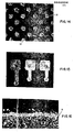
- Figs. 14 and 15 show the via regions and EC pads, of a sample, showing Pd/Ni coated molybdenum circuit features and the absence of any bridge in between the conductors.
- Fig. 16 shows a cross-section through a via 30 confirming the formation of a continuous adherent layer 14 of Pd/Ni alloy.
- the ultrasonic cleaning can be effected by conventional methods utilizing suitable mediums in a conventional tank type of cleaners having side and or bottom mounted transducers.
- the mechanism of film removal in ultrasonic cleaning involves the rupturing of the loose metal film areas 14A from the substrate areas by the action of the shock waves impinging on the surfaces.
- the shock waves being induced by bubble collapse (cavitation) within the liquid medium during the ultrasonic action.
- One preferred form of removing the metal film areas 14A is by use of an ultrasonic horn to focus and deliver very high local intensities of energy (about 100 watts per cm 2 ) and by utilizing the near field characteristics of the ultrasonic field close (e.g. about 1 to about 10 mm) to the horn surface where cavitation plays only a minor role.
- non-adhering palladium-nickel films of 5 gm thickness can be removed from alumina ceramic surfaces in about 5 to about 30 seconds.
- the mechanism of metal film removal is as follows: In the near-field region, there exists a coupling of the ultrasonic field (generated by the transducer) to the surface of the substrate carrying the metal film. Where the metal film 14 is strongly adhering to the substrate, such as in areas of the pre-existing metallurgical circuit features under the film, the ultrasonic energy is merely transmitted through the metal film 14 into the substrate and dissipated. Where the metal film 14 is non-adhering, such as on the bare substrate surface areas, the ultrasonic energy is substantially absorbed by the thin metal film 14, causing it to vibrate with the field. This vibration generates alternating stresses at points of the film where it adheres to the substrate which eventually causes the film breakage at these points.
- High frequencies (e.g. 10-40 KHz) of the field ensures that from 10-40 X I0 3 cycles of alternating stress is applied to the metal film 14 at the boundaries of adhering regions so that the fatigue limit for the film is reached (in 1 to 30 seconds) depending on the nature of the metal film, its thicknesses, and the distance between adjacent adhering areas.
- the fatigue limit for the film is reached (in 1 to 30 seconds) depending on the nature of the metal film, its thicknesses, and the distance between adjacent adhering areas.
Landscapes
- Chemical & Material Sciences (AREA)
- Engineering & Computer Science (AREA)
- Ceramic Engineering (AREA)
- Materials Engineering (AREA)
- Structural Engineering (AREA)
- Organic Chemistry (AREA)
- Inorganic Chemistry (AREA)
- Manufacturing & Machinery (AREA)
- Microelectronics & Electronic Packaging (AREA)
- Mechanical Engineering (AREA)
- Manufacturing Of Printed Wiring (AREA)
Applications Claiming Priority (4)
| Application Number | Priority Date | Filing Date | Title |
|---|---|---|---|
| US06/359,445 US4501768A (en) | 1982-03-18 | 1982-03-18 | Thin film floating zone metal coating technique |
| US06/359,469 US4493856A (en) | 1982-03-18 | 1982-03-18 | Selective coating of metallurgical features of a dielectric substrate with diverse metals |
| US359445 | 1982-03-18 | ||
| US359469 | 1982-03-18 |
Publications (2)
| Publication Number | Publication Date |
|---|---|
| EP0089604A1 true EP0089604A1 (fr) | 1983-09-28 |
| EP0089604B1 EP0089604B1 (fr) | 1986-12-17 |
Family
ID=27000484
Family Applications (1)
| Application Number | Title | Priority Date | Filing Date |
|---|---|---|---|
| EP83102539A Expired EP0089604B1 (fr) | 1982-03-18 | 1983-03-15 | Procédé pour le revêtement sélectif des échantillons métallurgiques se trouvant sur substrats diélectriques |
Country Status (2)
| Country | Link |
|---|---|
| EP (1) | EP0089604B1 (fr) |
| DE (1) | DE3368447D1 (fr) |
Cited By (7)
| Publication number | Priority date | Publication date | Assignee | Title |
|---|---|---|---|---|
| EP0185998A1 (fr) * | 1984-12-14 | 1986-07-02 | Dynamics Research Corporation | Fabrication de circuits d'interconnexion par électroformage de transfert |
| US4685030A (en) * | 1985-04-29 | 1987-08-04 | Energy Conversion Devices, Inc. | Surface mounted circuits including hybrid circuits, having CVD interconnects, and method of preparing the circuits |
| EP0265613A3 (en) * | 1986-10-27 | 1988-09-28 | International Business Machines Corporation | Method for repair of opens in thin film lines on a substrate |
| WO2008141481A1 (fr) | 2007-05-24 | 2008-11-27 | Princo Corp. | Structure et procédé de fabrication d'un câblage métallique sur une carte multicouches |
| US8815333B2 (en) | 2007-12-05 | 2014-08-26 | Princo Middle East Fze | Manufacturing method of metal structure in multi-layer substrate |
| WO2025108174A1 (fr) * | 2023-11-24 | 2025-05-30 | 四平市光华电子技术有限公司 | Procédé et appareil de fabrication de motif de coulée applicables à un circuit de précision |
| CN121358275A (zh) * | 2025-12-17 | 2026-01-16 | 合肥晶合集成电路股份有限公司 | 一种芯片的制备方法及芯片 |
Citations (4)
| Publication number | Priority date | Publication date | Assignee | Title |
|---|---|---|---|---|
| US3945113A (en) * | 1973-03-02 | 1976-03-23 | Thomson-Csf | Method for manufacturing a connecting circuit for an integrated miniaturised wiring system |
| DE2443287B2 (de) * | 1974-09-10 | 1977-03-24 | Siemens AG, 1000 Berlin und 8000 München | Verfahren zum herstellen einer multichip-verdrahtung |
| DE2745581A1 (de) * | 1976-12-10 | 1978-06-15 | Ibm | Verfahren zum herstellen mehrschichtiger keramischer substrate |
| DE2453035B2 (de) * | 1973-12-20 | 1981-04-16 | International Business Machines Corp., 10504 Armonk, N.Y. | Verfahren zum Aufbringen einer metallischen Schicht in Form eines Musters auf einem mit einer ersten dünnen, metallischen Schicht überzogenen inerten Substrat |
-
1983
- 1983-03-15 DE DE8383102539T patent/DE3368447D1/de not_active Expired
- 1983-03-15 EP EP83102539A patent/EP0089604B1/fr not_active Expired
Patent Citations (4)
| Publication number | Priority date | Publication date | Assignee | Title |
|---|---|---|---|---|
| US3945113A (en) * | 1973-03-02 | 1976-03-23 | Thomson-Csf | Method for manufacturing a connecting circuit for an integrated miniaturised wiring system |
| DE2453035B2 (de) * | 1973-12-20 | 1981-04-16 | International Business Machines Corp., 10504 Armonk, N.Y. | Verfahren zum Aufbringen einer metallischen Schicht in Form eines Musters auf einem mit einer ersten dünnen, metallischen Schicht überzogenen inerten Substrat |
| DE2443287B2 (de) * | 1974-09-10 | 1977-03-24 | Siemens AG, 1000 Berlin und 8000 München | Verfahren zum herstellen einer multichip-verdrahtung |
| DE2745581A1 (de) * | 1976-12-10 | 1978-06-15 | Ibm | Verfahren zum herstellen mehrschichtiger keramischer substrate |
Cited By (8)
| Publication number | Priority date | Publication date | Assignee | Title |
|---|---|---|---|---|
| EP0185998A1 (fr) * | 1984-12-14 | 1986-07-02 | Dynamics Research Corporation | Fabrication de circuits d'interconnexion par électroformage de transfert |
| US4685030A (en) * | 1985-04-29 | 1987-08-04 | Energy Conversion Devices, Inc. | Surface mounted circuits including hybrid circuits, having CVD interconnects, and method of preparing the circuits |
| EP0265613A3 (en) * | 1986-10-27 | 1988-09-28 | International Business Machines Corporation | Method for repair of opens in thin film lines on a substrate |
| WO2008141481A1 (fr) | 2007-05-24 | 2008-11-27 | Princo Corp. | Structure et procédé de fabrication d'un câblage métallique sur une carte multicouches |
| EP2161973A4 (fr) * | 2007-05-24 | 2011-08-03 | Princo Corp | Structure et procédé de fabrication d'un câblage métallique sur une carte multicouches |
| US8815333B2 (en) | 2007-12-05 | 2014-08-26 | Princo Middle East Fze | Manufacturing method of metal structure in multi-layer substrate |
| WO2025108174A1 (fr) * | 2023-11-24 | 2025-05-30 | 四平市光华电子技术有限公司 | Procédé et appareil de fabrication de motif de coulée applicables à un circuit de précision |
| CN121358275A (zh) * | 2025-12-17 | 2026-01-16 | 合肥晶合集成电路股份有限公司 | 一种芯片的制备方法及芯片 |
Also Published As
| Publication number | Publication date |
|---|---|
| EP0089604B1 (fr) | 1986-12-17 |
| DE3368447D1 (en) | 1987-01-29 |
Similar Documents
| Publication | Publication Date | Title |
|---|---|---|
| US4493856A (en) | Selective coating of metallurgical features of a dielectric substrate with diverse metals | |
| EP0089559B1 (fr) | Procédé pour fabriquer des couches métalliques pour configurations métallurgiques sur des substrats diélectriques | |
| CN101687284B (zh) | 接合体及其制造方法、以及功率半导体模块及其制造方法 | |
| US8299604B2 (en) | Bonded metal and ceramic plates for thermal management of optical and electronic devices | |
| EP0607732A2 (fr) | Structure et procédé pour une barrière de diffusion entre un métal noble et un métal non-noble | |
| KR100304993B1 (ko) | 범프형집적회로패키지용막회로금속시스템 | |
| EP0265613A2 (fr) | Méthode pour réparer des discontinuités dans des couches minces sur un substrat | |
| US5731066A (en) | Electronic circuit device | |
| US4504322A (en) | Re-work method for removing extraneous metal from cermic substrates | |
| US5787578A (en) | Method of selectively depositing a metallic layer on a ceramic substrate | |
| EP0089604B1 (fr) | Procédé pour le revêtement sélectif des échantillons métallurgiques se trouvant sur substrats diélectriques | |
| US4501768A (en) | Thin film floating zone metal coating technique | |
| US6742248B2 (en) | Method of forming a soldered electrical connection | |
| JPH10510098A (ja) | 酸化しやすく鑞付け可能な金属サブストレート上に導線をボンディングするための方法 | |
| EP0717125A1 (fr) | Liaison de diamant sur un substrat | |
| US6645606B2 (en) | Electrical device having metal pad bonded with metal wiring and manufacturing method thereof | |
| JP3470789B2 (ja) | 配線基板及びその製造方法 | |
| JPS62222060A (ja) | スパツタリング用タ−ゲツト | |
| JPH03218644A (ja) | 回路基板の接続構造 | |
| US6884708B2 (en) | Method of partially plating substrate for electronic devices | |
| JPH06199579A (ja) | 金属部材とセラミック部材との接合方法 | |
| JP2004146444A (ja) | 配線基板 | |
| JPS6366949A (ja) | はんだバンブの形成方法 | |
| JPH08330495A (ja) | 配線基板 | |
| JP2004140108A (ja) | 配線基板 |
Legal Events
| Date | Code | Title | Description |
|---|---|---|---|
| PUAI | Public reference made under article 153(3) epc to a published international application that has entered the european phase |
Free format text: ORIGINAL CODE: 0009012 |
|
| AK | Designated contracting states |
Designated state(s): DE FR GB |
|
| 17P | Request for examination filed |
Effective date: 19840126 |
|
| GRAA | (expected) grant |
Free format text: ORIGINAL CODE: 0009210 |
|
| AK | Designated contracting states |
Kind code of ref document: B1 Designated state(s): DE FR GB |
|
| ET | Fr: translation filed | ||
| REF | Corresponds to: |
Ref document number: 3368447 Country of ref document: DE Date of ref document: 19870129 |
|
| PLBE | No opposition filed within time limit |
Free format text: ORIGINAL CODE: 0009261 |
|
| STAA | Information on the status of an ep patent application or granted ep patent |
Free format text: STATUS: NO OPPOSITION FILED WITHIN TIME LIMIT |
|
| 26N | No opposition filed | ||
| PGFP | Annual fee paid to national office [announced via postgrant information from national office to epo] |
Ref country code: GB Payment date: 19930216 Year of fee payment: 11 |
|
| PGFP | Annual fee paid to national office [announced via postgrant information from national office to epo] |
Ref country code: FR Payment date: 19930226 Year of fee payment: 11 |
|
| PGFP | Annual fee paid to national office [announced via postgrant information from national office to epo] |
Ref country code: DE Payment date: 19930406 Year of fee payment: 11 |
|
| PG25 | Lapsed in a contracting state [announced via postgrant information from national office to epo] |
Ref country code: GB Effective date: 19940315 |
|
| GBPC | Gb: european patent ceased through non-payment of renewal fee |
Effective date: 19940315 |
|
| PG25 | Lapsed in a contracting state [announced via postgrant information from national office to epo] |
Ref country code: FR Effective date: 19941130 |
|
| PG25 | Lapsed in a contracting state [announced via postgrant information from national office to epo] |
Ref country code: DE Effective date: 19941201 |
|
| REG | Reference to a national code |
Ref country code: FR Ref legal event code: ST |