EP0089681A1 - Auskoppelschaltung - Google Patents
Auskoppelschaltung Download PDFInfo
- Publication number
- EP0089681A1 EP0089681A1 EP83102850A EP83102850A EP0089681A1 EP 0089681 A1 EP0089681 A1 EP 0089681A1 EP 83102850 A EP83102850 A EP 83102850A EP 83102850 A EP83102850 A EP 83102850A EP 0089681 A1 EP0089681 A1 EP 0089681A1
- Authority
- EP
- European Patent Office
- Prior art keywords
- divider
- resistor
- output
- input
- differential amplifier
- Prior art date
- Legal status (The legal status is an assumption and is not a legal conclusion. Google has not performed a legal analysis and makes no representation as to the accuracy of the status listed.)
- Granted
Links
Images
Classifications
-
- H—ELECTRICITY
- H04—ELECTRIC COMMUNICATION TECHNIQUE
- H04B—TRANSMISSION
- H04B3/00—Line transmission systems
- H04B3/54—Systems for transmission via power distribution lines
- H04B3/548—Systems for transmission via power distribution lines the power on the line being DC
-
- H—ELECTRICITY
- H02—GENERATION; CONVERSION OR DISTRIBUTION OF ELECTRIC POWER
- H02J—ELECTRIC POWER NETWORKS; CIRCUIT ARRANGEMENTS OR SYSTEMS FOR SUPPLYING OR DISTRIBUTING ELECTRIC POWER; SYSTEMS FOR STORING ELECTRIC ENERGY
- H02J13/00—Circuit arrangements for providing remote monitoring or remote control of equipment in a power distribution network
- H02J13/13—Circuit arrangements for providing remote monitoring or remote control of equipment in a power distribution network characterised by the transmission of data to equipment in the power network
- H02J13/1311—Circuit arrangements for providing remote monitoring or remote control of equipment in a power distribution network characterised by the transmission of data to equipment in the power network using the power network as support for the transmission
- H02J13/1313—Circuit arrangements for providing remote monitoring or remote control of equipment in a power distribution network characterised by the transmission of data to equipment in the power network using the power network as support for the transmission using pulsed signals
-
- H—ELECTRICITY
- H04—ELECTRIC COMMUNICATION TECHNIQUE
- H04B—TRANSMISSION
- H04B3/00—Line transmission systems
- H04B3/54—Systems for transmission via power distribution lines
- H04B3/56—Circuits for coupling, blocking, or by-passing of signals
-
- H—ELECTRICITY
- H02—GENERATION; CONVERSION OR DISTRIBUTION OF ELECTRIC POWER
- H02M—APPARATUS FOR CONVERSION BETWEEN AC AND AC, BETWEEN AC AND DC, OR BETWEEN DC AND DC, AND FOR USE WITH MAINS OR SIMILAR POWER SUPPLY SYSTEMS; CONVERSION OF DC OR AC INPUT POWER INTO SURGE OUTPUT POWER; CONTROL OR REGULATION THEREOF
- H02M7/00—Conversion of AC power input into DC power output; Conversion of DC power input into AC power output
- H02M7/02—Conversion of AC power input into DC power output without possibility of reversal
- H02M7/04—Conversion of AC power input into DC power output without possibility of reversal by static converters
- H02M7/05—Capacitor coupled rectifiers
-
- H—ELECTRICITY
- H04—ELECTRIC COMMUNICATION TECHNIQUE
- H04B—TRANSMISSION
- H04B2203/00—Indexing scheme relating to line transmission systems
- H04B2203/54—Aspects of powerline communications not already covered by H04B3/54 and its subgroups
- H04B2203/5462—Systems for power line communications
- H04B2203/547—Systems for power line communications via DC power distribution
-
- Y—GENERAL TAGGING OF NEW TECHNOLOGICAL DEVELOPMENTS; GENERAL TAGGING OF CROSS-SECTIONAL TECHNOLOGIES SPANNING OVER SEVERAL SECTIONS OF THE IPC; TECHNICAL SUBJECTS COVERED BY FORMER USPC CROSS-REFERENCE ART COLLECTIONS [XRACs] AND DIGESTS
- Y02—TECHNOLOGIES OR APPLICATIONS FOR MITIGATION OR ADAPTATION AGAINST CLIMATE CHANGE
- Y02B—CLIMATE CHANGE MITIGATION TECHNOLOGIES RELATED TO BUILDINGS, e.g. HOUSING, HOUSE APPLIANCES OR RELATED END-USER APPLICATIONS
- Y02B90/00—Enabling technologies or technologies with a potential or indirect contribution to GHG emissions mitigation
- Y02B90/20—Smart grids as enabling technology in buildings sector
-
- Y—GENERAL TAGGING OF NEW TECHNOLOGICAL DEVELOPMENTS; GENERAL TAGGING OF CROSS-SECTIONAL TECHNOLOGIES SPANNING OVER SEVERAL SECTIONS OF THE IPC; TECHNICAL SUBJECTS COVERED BY FORMER USPC CROSS-REFERENCE ART COLLECTIONS [XRACs] AND DIGESTS
- Y02—TECHNOLOGIES OR APPLICATIONS FOR MITIGATION OR ADAPTATION AGAINST CLIMATE CHANGE
- Y02E—REDUCTION OF GREENHOUSE GAS [GHG] EMISSIONS, RELATED TO ENERGY GENERATION, TRANSMISSION OR DISTRIBUTION
- Y02E60/00—Enabling technologies; Technologies with a potential or indirect contribution to GHG emissions mitigation
-
- Y—GENERAL TAGGING OF NEW TECHNOLOGICAL DEVELOPMENTS; GENERAL TAGGING OF CROSS-SECTIONAL TECHNOLOGIES SPANNING OVER SEVERAL SECTIONS OF THE IPC; TECHNICAL SUBJECTS COVERED BY FORMER USPC CROSS-REFERENCE ART COLLECTIONS [XRACs] AND DIGESTS
- Y04—INFORMATION OR COMMUNICATION TECHNOLOGIES HAVING AN IMPACT ON OTHER TECHNOLOGY AREAS
- Y04S—SYSTEMS INTEGRATING TECHNOLOGIES RELATED TO POWER NETWORK OPERATION, COMMUNICATION OR INFORMATION TECHNOLOGIES FOR IMPROVING THE ELECTRICAL POWER GENERATION, TRANSMISSION, DISTRIBUTION, MANAGEMENT OR USAGE, i.e. SMART GRIDS
- Y04S40/00—Systems for electrical power generation, transmission, distribution or end-user application management characterised by the use of communication or information technologies, or communication or information technology specific aspects supporting them
- Y04S40/12—Systems for electrical power generation, transmission, distribution or end-user application management characterised by the use of communication or information technologies, or communication or information technology specific aspects supporting them characterised by data transport means between the monitoring, controlling or managing units and monitored, controlled or operated electrical equipment
- Y04S40/121—Systems for electrical power generation, transmission, distribution or end-user application management characterised by the use of communication or information technologies, or communication or information technology specific aspects supporting them characterised by data transport means between the monitoring, controlling or managing units and monitored, controlled or operated electrical equipment using the power network as support for the transmission
Definitions
- the invention relates to an outcoupling circuit for an audio frequency ripple control receiver with a capacitor power supply in a full-wave rectifier design with a series capacitor, a protective impedance circuit and a surge arrester circuit being provided on the network input side and a Zener diode circuit being provided on the rectifier output side or in the full-wave rectifier, and with one the output of the capacitor power supply connected charging capacitor.
- a capacitor power supply with full-wave rectification when used in a ripple control receiver, has difficulties due to mixing in the full-wave rectifier and in the filter input.
- sine waves cut off at the AC voltage connections compared to the DC voltage connections occur, the voltage being limited by a Zener diode circuit. If a DC voltage connection is now taken as ground and the audio frequency is taken off, for example, upstream of the series capacitor, the voltage controlling the filter is superimposed or disturbed by the above-mentioned cut-off sine wave with considerable amplitude. It is disadvantageous that the use of non-linear components in the mains rectifier and in amplifier stages leads to non-linear distortions and thus to the occurrence of mixed frequencies.
- the pass frequency of the downstream filter results in an ambiguity of the response behavior with regard to the frequency, which in turn gives rise to malfunctions and in particular can result in an undesired incorrect switching of the ripple control receiver.
- AT-PS 326.756 describes a power supply part for an electronic ripple control receiver with a rectifier connected to the AC network via a capacitor and to which a voltage stabilizer is assigned, in which the capacitor has a voltage protection impedance, e.g. a surge-proof resistor, a surge-proof inductor or a series circuit of a surge-proof inductor and a resistor is connected upstream.
- a voltage protection impedance e.g. a surge-proof resistor, a surge-proof inductor or a series circuit of a surge-proof inductor and a resistor is connected upstream.
- AT-PS 352.209 describes a circuit arrangement for a remote control receiver connected to a power supply network, to which remote control signals are supplied via the power supply network, in particular a ripple control receiver, with a frequency-selective receiving part, an evaluation part assigned to it and a switching element connected downstream thereof, the remote control receiver having one has the input circuit of the frequency-selective receiving part coupled with a non-linear switching power supply part, which is flowed through by currents of several frequencies, between the receiver input and the input of the selective receiving part at least one circuit for compensating for the mixed products from the mains frequency caused by the non-linear switching element in the power supply part, their harmonics and remote control signal vibrations supplied to the receiver from the power grid is arranged.
- the disadvantage here is that the frequency-selective circuit part must be carried out with a differential input and that the Ausge design of the input element depends on the design of the frequency-selective circuit.
- the invention has for its object to tap the control voltage for the downstream filter from a point at which it is undistorted and, moreover, is not separated from the voltage source by components with a non-linear characteristic, in particular by rectifiers.
- the design of the frequency-selective circuit should be independent of the design of the input element.
- a decoupling stage which is frequency-independent in the working range and consists of a differential amplifier connected directly to the charging capacitor in terms of power supply, is connected to the charging capacitor, the first input of which is connected to the dividing point of a first voltage divider, the first dividing resistor of which is connected to the phase-side power terminal and the second divider resistor is connected to the ground potential of the charging ⁇ capacitor, that the second input of the differential amplifier is connected to the divider point of a second voltage divider, the first divider resistor of which is connected to the mains terminal on the center or neutral side, and the second divider resistor of which Ground potential of the charging capacitor is connected that the divider ratios of the first voltage divider and the second voltage divider are the same for optimal compensation and that as A Output for the sound frequency signal from the decoupling stage serves the output of the differential amplifier.
- the use of the decoupling stage enables the frequency response to be unambiguous, that the use of a downstream filter with only one input is possible and that a differential input is not required there, and moreover the component expenditure remains low.
- the dimensioning of a filter to be connected downstream of the decoupling circuit is independent of the decoupling circuit and can thus be optimized for the filter function. There is no influence by the cut-off sinusoidal oscillation from the rectifier as the controlling voltage of the filter, whereby mixtures resulting from a potential difference between the neutral conductor and ground must be compensated for.
- the compensation advantageously takes place in that the interference voltage present at one input of the differential amplifier is compensated for via the second input of the differential amplifier and no longer appears as a control voltage for the differential amplifier.
- the audio frequency ripple control receiver does not work with the neutral conductor, but with ground as the supply pole.
- the differential amplifier can be a negative-coupled operational amplifier, the non-inverting input of which is the second input of the differential amplifier and the inverting input of which is connected to the first input of the differential amplifier via a series resistor and to the output of the operational amplifier via a negative feedback resistor, the series resistor at the dimensioning of the divider ratio of the first voltage divider is also taken into account. It is advantageous that the operational amplifier is largely independent of semiconductor tolerances and that an economical and compact embodiment can be achieved in connection with a further overall circuit by using multiple operational amplifiers.
- the differential amplifier can also be a base-controlled transistor, the base of the transistor having the division point of the first voltage divider and is connected via a base series resistor to the supply voltage potential of the charging capacitor, the emitter of the transistor being connected to the dividing point of the second voltage divider and the collector of the transistor being connected to the ground potential of the charging capacitor via a collector resistor, the collector of the Transistor represents the output of the differential amplifier and the base series resistor and the resistances of the respective transistor paths are also taken into account when dimensioning the divider ratios.
- the first voltage divider is connected to the input capacitor side input of the full-wave rectifier.
- the separation from the network by the series capacitor is advantageous here.
- the first voltage divider can be connected to the phase-side power terminal via a protective resistor of the protective impedance circuit.
- the second voltage divider can also be connected via a protective resistor of the protective impedance circuit to the mains terminal on the center or neutral side. The decoupling circuit is thus also protected by the protective impedance circuit.
- a protective impedance R 1 or R 2 is connected to the network terminals R and N, which form the protective impedance circuit, the respective presence of which, however, is not mandatory.
- Matternapssableiterbesciens VOR which is connected to the protective impedances R 1 and R 2, and of a series connection of a ballast capacitor C1 and a rectifier bridge D 1, D 2, D 3, D 4 g parallel e-switched on.
- the series capacitor C is connected on the phase side.
- a parallel circuit comprising a Zender diode D 5 and a charging capacitor C 2 is connected to the bridge output of the rectifier bridge D 1 , D 2 , D3, D 4 , the Zener diode D 5 being connected to the rectifier bridge D 1 , D 2 , D 39 D by a corresponding connection 4 can be replaced by means of Zener diodes.
- an operational amplifier 0 1 is connected in parallel to the charging capacitor C 2 in terms of power supply.
- the inverting input of the operational amplifier O 1 is connected via a series resistor R 5 to the dividing point of a voltage divider, the one divider resistor R 3 being connected to the phase-side protective impedance R 1 of the protective impedance circuit for the control signal supply, and the second divider resistor R 4 to the ground-side terminal of the charging capacitor C 2 is connected.
- the non-inverting input of the operational amplifier O 1 is connected to the divider point of a further voltage divider, the one further divider resistor R 6 being connected to the protective impedance R 2 on the center or neutral side, and the second further divider resistor R 7 being connected to the ground-side terminal of the charging capacitor C 2 is connected.
- the protective impedances R 1 , R 2 provided in one or both phases serve as protection against shock waves.
- the output of the operational amplifier O 1 serves as the signal output A of the decoupling circuit.
- the mains voltage and the audio frequency voltage superimposed on it are fed in at the mains terminals R, N.
- the downstream capacitor power supply is used to supply the audio frequency ripple control receiver.
- the effect of the rectifier bridge D 1 , D 2 , D 3 , D 4 on the rectifier D 3 of this bridge results in a cut-off sine wave which is superimposed on the voltage applied to the network terminals R, N.
- This voltage occurs in accordance with the divider ratio of one voltage divider R 39 R 4 and R 5 at the inverting input of the operational amplifier 0 1 .
- the disturbing voltage occurring at the rectifier D 3 in relation to ground is fed via the further voltage divider R 6 , R 7 to the non-inverting input of the operational amplifier 0 1 .
- the disturbing voltage at the rectifier D 3 no longer occurs as a controlling voltage and cannot result in any mixed products there either.
- the audio frequency signal can therefore be removed in an undistorted or unambiguous form.
- Optimal signal conditions according to the invention can be achieved if the divider ratios of the one voltage divider connected to the inverting input, including the series resistor R 5 and the one to the non-inverting input connected further voltage divider are the same size.
- the controlling voltage of the operational amplifier 0 1 is, in a first approximation, independent of the voltage of the neutral or center conductor relative to the second pole of the supply for the charging capacitor (generally ground) and with a suitable design of the coupling is therefore not influenced by the interference caused by mixing.
- the terminals plus and minus on the output side are also provided for the power supply of the further electronics, for example a filter F.
- the operational amplifier O 1 is replaced by a transistor T 1 .
- the series connection of a collector resistor R 7 , a transistor T 1 and an emitter resistor R 8 is connected in parallel with the charging capacitor C 2 .
- the charging capacitor C 2 has a base voltage divider, consisting of a resistor R 5 and a further resistor R 6, connected in parallel.
- the emitter of transistor T 1 is connected via a resistor R 4 to the neutral or. protective impedance R 2 connected on the center conductor side.
- the base control of the transistor takes place via a series resistor R 3 , which is connected to the phase-side protective impedance R 1 .
- the series resistor R 3 can also be connected directly to the mains terminal R, whereby it should be taken into account that in the absence of the protective impedance R 1 there is no shock wave protection of the downstream filter.
- the series resistor R 3 could also be connected directly to the rectifier input at g D 1 , D2 , D39 D4 after the series capacitor C 1 , with increased interference from modulation interference by the mains rectifier being accepted here are.
- the control signal tap for the decoupling stage as the most direct possible connection to the network tap has the advantage that the audio frequency occurs most authentically there.
- the protective impedances R 1 , R 2 provided in one or both phases serve as protection against shock waves.
- the signal output A of the decoupling circuit is connected to the collector of transistor D 1 .
- a cut-off sine wave occurs due to the action of the rectifier bridge on the rectifier D 3 , which is related to ground and is superimposed on the voltage applied to the network terminals R and N.
- This voltage occurs according to the division ratio of the resistors R 32 R 5 and R 6 at the base input.
- the disturbing voltage occurring at the rectifier D 3 in relation to ground is fed to the emitter via the voltage divider from the resistors R 4 , R 8 .
- the disturbing voltage at the rectifier D 3 therefore no longer occurs as a controlling voltage at the base-emitter diode of the transistor T 1 and cannot result in any mixed products there.
- the audio frequency signal on the collector can therefore be removed in an undistorted or unambiguous form.
- Optimal signal ratios can be achieved if the divider ratios from the voltage dividers emitter resistor R 8 to voltage divider resistor R 4 and from the resistors R 5 , R 6 of the base voltage divider to the series resistor R 3 are the same, taking into account the transistor input resistances.
- Line-like design of the decoupling circuit is also possible in an analog manner with a transistor of the pnp type.
Landscapes
- Engineering & Computer Science (AREA)
- Power Engineering (AREA)
- Computer Networks & Wireless Communication (AREA)
- Signal Processing (AREA)
- Rectifiers (AREA)
- Amplifiers (AREA)
- Oscillators With Electromechanical Resonators (AREA)
Abstract
Description
- Die Erfindung betrifft eine Auskoppelschaltung für einen Tonfrequenz-Rundsteuer-Empfänger mit einem Kondensatornetzgerät in Vollweg-Gleichrichterausführung mit Vorschaltkondensator, wobei netzeingangsseitig eine Schutzimpedanzbeschaltung sowie eine Uberspannungsableiterbeschaltung vorsehbar ist und wobei gleichrichterausgangsseitig bzw. im Vollweg-Gleichrichter selbst eine Zenerdiodenschaltung vorsehbar ist, sowie mit einem an den Ausgang des Kondensatornetzgerätes angeschlossenen Ladekondensator.
- Bei einem Kondensatornetzteil mit Vollweg-Gleichrichtung treten bei Verwendung in einem Rundsteuerempfänger Schwierigkeiten durch Mischung im Vollweg-Gleichrichter und im Filtereingang auf. Bei der Gleichrichter-Brückenschaltung treten an den Wechselspannungsanschlüssen gegenüber den Gleichspannungsanschlüssen abgekappte Sinusschwingungen auf, wobei durch eine Zenerdiodenbeschaltung die Spannung begrenzt ist. Wird nun ein Gleichspannungsanschluß als Masse genommen und die Tonfrequenz beispielsweise vor dem Vorschaltkondensator abgenommen, so ist die das Filter aussteuernde Spannung von der oben erwähnten abgekappten Sinusschwingung mit erheblicher Amplitude überlagert bzw. gestört. Nachteilig ist, daß es durch die Verwendung von nichtlinearen Bauelementen im Netzgleichrichter sowie in Verstärkerstufen zu nichtlinearen Verzerrungen und somit zum Auftreten von Mischfrequenzen kommt. Tritt-nun eine Tonfrequenz auf, die mit einer zweiten Frequenz, z.B. der Netzfrequenz oder auch Oberwellen der Netzfrequenz gemischt, die Durchlaßfrequenz des nachgeschalteten Filters ergibt, so ist eine Mehrdeutigkeit des Ansprechverhaltens bezüglich der Frequenz gegeben, was wiederum zu Störungen Anlaß gibt und insbesondere ein unerwünschtes Fehlschalten des Rundsteuerempfängers zur Folge haben kann.
- In der AT-PS 326.756 wird ein Stromversorgungsteil für einen elektronischen Rundsteuerempfänger mit einem über einen Kondensator an das Wechselstromnetz angeschlossenen Gleichrichter, dem ein Spannungsstabilisator zugeordnet ist, beschrieben, bei dem dem Kondensator eine Spannungsschutzimpedanz, z.B. ein stoßspannungsfester Widerstand, eine stoßspannungsfeste Induktivität oder eine Serienschaltung einer stoßspannungsfesten Induktivität und eines Widerstandes vorgeschaltet ist.
- In der AT-PS 352.209 wird eine Schaltungsanordnung für einen an ein Starkstromnetz angeschlossenen Fernsteuerempfänger beschrieben, dem Fernsteuersignale über das Starkstromnetz zugeführt werden, insbesondere einen Rundsteuerempfänger, mit einem frequenzselektiven Empfangsteil, einem diesem zugeordneten Auswerteteil und einem diesen nachgeschalteten Schaltorgan, wobei der Fernsteuerempfänger einen mit dem Eingangskreis des frequenzselektiven Empfangsteiles gekoppelten, mit einem nichtlinearen Schaltelement versehenen Stromversorgungsteil aufweist, der von Strömen mehrerer Frequenzen durchflossen ist, wobei zwischen dem Empfängereingang und dem Eingang des selektiven Empfangsteiles mindestens ein Schaltkreis zur Kompensation der durch das nichtlineare Schaltelement im Stromversorgungsteil verursachtaiMischprodukte aus der Netzfrequenz, ihren Harmonischen und vom Starkstromnetz dem Empfänger zugeführten Fernsteuersignalschwingungen angeordnet ist. Nachteilig ist hierbei, daß der frequenzselektive Schaltungsteil mit einem Differenzeingang ausgeführt werden muß und daß die Ausgestaltung des Eingangsgliedes abhängig von der Auslegung der frequenzselektiven Schaltung ist.
- Der Erfindung liegt die Aufgabe zugrunde, die Steuerspannung für das nachgeschaltete Filter von einer Stelle abzugreifen, an der sie unverzerrt und überdies durch keine Bauelemente mit nichtlinearer Kennlinie, insbesondere durch Gleichrichter, von der Spannungsquelle getrennt ist. Dabei soll die Auslegung der frequenzselektiven Schaltung unabhängig von der Auslegung des Eingangsgliedes sein.
- Diese Aufgabe wird erfindungsgemäß dadurch gelöst, daß an den Ladekondensator eine im Arbeitsbereich frequenzunabhängige Auskoppelstufe, bestehend aus einem stromversorgungsmäßig direkt mit dem Ladekondensator verbundenen Differenzverstärker angeschlossen ist, dessen erster Eingang an den Teilerpunkt eines ersten Spannungsteilers angeschlossen ist, dessen erster Teilerwiderstand an die phasenseitige Netzklemme angeschlossen ist und dessen zweiter Teilerwiderstand an das Massepotential des Lade- <kondensators angeschlossen ist, daß der zweite Eingang des Differenzverstärkers an den Teilerpunkt eines zweiten Spannungsteilers angeschlossen ist, dessen erster Teilerwiderstand an die mittelpunkts- bzw. nulleiterseitige Netzklemme angeschlossen ist und dessen zweiter Teilerwiderstand an das Massepotential des Ladekondensators angeschlossen ist, daß die Teilerverhältnisse des ersten Spannungsteilers und des zweiten Spannungsteilers für eine optimale Kompensation gleich groß sind und daß als Ausgang für das tonfrequente Signal aus der Auskoppelstufe der Ausgang des Differenzverstärkers dient. Vorteilhaft ist, daß durch die Verwendung der Auskoppelstufe eine Eindeutigkeit des Frequenzverhaltens erzielbar ist, daß die Verwendung eines nachgeschalteten Filters mit nur einem Eingang möglich ist und ein Differenzeingang dort nicht erforderlich ist, wobei außerdem der Bauteileaufwand gering bleibt. Die Dimensionierung eines der Auskoppelschaltung nachzuschaltenden Filters ist unabhängig von der Auskoppelschaltung und kann somit für die Filterfunktion optimiert werden. Es erfolgt keine Beeinflussung durch die abgekappte Sinusschwingung vom Gleichrichter als steuernde Spannung des Filters, wobei Mischungen, die durch einen Potentialunterschied zwischen Nulleiter und Masse entstehen, zu kompensieren sind. Die Kompensation erfolgt vorteilhafterweise dadurch, daß die am einen Eingang des Differenzverstärkers anstehende Störspannung über den zweiten Eingang des Differenzverstärkers kompensiert wird und nicht mehr als steuernde Spannung für den Differenzverstärker in Erscheinung tritt. Der Tonfrequenz-Rundsteuer-Empfänger arbeitet nicht mit dem Nulleiter, sondern mit Masse als Versorgungspol.
- In einer vorteilhaften Ausführungsform kann der Differenzverstärker ein gegengekoppglter Operationsverstärker sein, dessen nichtinvertierender Eingang der zweite Eingang des Differenzverstärkers ist und dessen invertierender Eingang über einen Vorwiderstand mit dem ersten Eingang des Differenzverstärkers und über einen Gegenkopplungswiderstand mit dem Ausgang des Operationsverstärkers verbunden ist, wobei der Vorwiderstand bei der Bemessung des Teilerverhältnisses des ersten Spannungsteilers mit berücksichtigt ist. Dabei ist vorteilhaft, daß durch den Operationsverstärker eine weitgehende Unabhängigkeit von Halbleitertoleranzen gegeben ist und daß im Zusammenhang mit einer weiteren Gesamtschaltung durch Verwendung von Mehrfach-Operationsverstärkern eine wirtschaftliche und kompakte Ausführungsform zu erzielen ist.
- In einer alternativen Ausführungsform kann der Differenzverstärker auch ein basisgesteuerter Transistor sein, wobei die Basis des Transistors mit dem Teilerpunkt des ersten Spannungsteilers und über einen Basis-Vorwiderstand mit dem Versorgungsspannungspotential des Ladekondensators verbunden ist, wobei der Emitter des Transistors an den Teilerpunkt des zweiten Spannungsteilers angeschlossen ist und wobei der Kollektor des Transistors über einen Kollektorwiderstand mit dem Massepotential des Ladekondensators verbunden ist, wobei der Kollektor des Transistors den Ausgang des Differenzverstärkers darstellt und wobei bei der Bemessung der Teilerverhältnisse der Basis-Vorwiderstand und die Widerstände der jeweiligen Transistorstrecken mit berücksichtigt werden.
- Bei einer vorteilhaften Ausführungsform der Erfindung ist der erste Spannungsteiler an den vorschaltkondensatorseitigen Eingang des Vollweg-Gleichrichters angeschlossen. Vorteilhaft ist hierbei die Trennung vom Netz durch den Vorschaltkondensator.
- Der erste Spannungsteiler kann über einen Schutzwiderstand der Schutzimpedanzbeschaltung an die phasenseitige Netzklemme angeschlossen sein. Auch der zweite Spannungsteiler kann über einen Schutzwiderstand der Schutzimpedanzbeschaltung mit der mittelpunkt- bzw. nulleiterseitigen Netzklemme verbunden sein. Damit wird auch die Auskoppelschaltung durch die Schutzimpedanzbeschaltung geschützt.
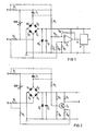
- Ausführungsbeispiele der Erfindung werden nachfolgend anhand der Figuren 1 und 2 näher erläutert. )
- In Fig. 1 ist ein an die Netzklemmen R (Phase) bzw. N (Mittelpunkt- oder Nulleiter) angeschlossenes Kondensatornetzgerät samt der Auskoppelstufe dargestellt. An die Netzklemmen R und N ist jeweils eine Schutzimpedanz R1 bzw. R2 angeschaltet, die die Schutzimpedanzbeschaltung bilden, deren jeweiliges Vorhandensein jedoch nicht zwingend ist. Ebenso nur fakultativ vorgesehen ist eine Überspannungsableiterbeschaltung VOR, die an die Schutzimpedanzen R1 und R2 angeschlossen ist, und zu der eine Serienschaltung aus einem Vorschaltkondensator C1 und einer Gleichrichterbrücke D1, D2, D3, D4 parallel ge-schaltet ist. Der Vorschaltkondensator C ist dabei phasenseitig angeschlossen. An den Brückenausgang der Gleichrichterbrücke D1, D2, D3, D4 ist eine Parallelschaltung aus einer Zenderdiode D5 und einem Ladekondensator C2 angeschlossen, wobei die Zenerdiode D5 durch eine entsprechende Beschaltung der Gleichrichterbrücke D1, D2, D39 D4 mittels Zenerdioden ersetzbar ist. Erfindungsgemäß ist dem Ladekondensator C2 stromversorgungsmäßig ein Operationsverstärker 01 parallel geschaltet. Der invertierende Eingang des Operationsverstärkers O1 ist über einen Vorwiderstand R5 an den Teilerpunkt eines Spannungsteilers angeschlossen, wobei für die Steuersignalzuführung der eine Teilerwiderstand R3 im weiteren an die phasenseitige Schutzimpedanz R1 der Schutzimpedanzbeschaltung angeschlossen ist und wobei der zweite Teilerwiderstand R4 an die masseseitige Klemme des Ladekondensators C2 angeschlossen ist. Der nichtinvertierende Eingang des Operationsverstärkers O1 ist an den Teilerpunkt eines weiteren Spannungsteilers angeschlossen, wobei der eine weitere Teilerwiderstand R6 an die mittelpunkts- bzw. nulleiterseitige Schutzimpedanz R2 der Schutzimpedanzbeschaltung angeschlossen ist, und wobei der zweite weitere Teilerwiderstand R7 an die masseseitige Klemme des Ladekondensators C2 angeschlossen ist. Als Gegenkopplung für den Operationsverstärker O1 ist zwischen Ausgang und invertierendem Eingang des Operationsverstärkers O1 ein Gegenkopplungswiderstand R8 geschaltet. Weitere Anschlußmöglichkeiten (strichliert gezeichnet) für die Steuerung bestehen direkt an der Netzklemme R, wobei zu berücksichtigen wäre, daß bei Fehlen der Schutzimpedanz R1 ein Stoßwellenschutz des nachgeschalteten Filters vorliegt, sowie direkt am Gleichrichtereingang D1, D2, D3, D4 nach dem Vorschaltkondensator C1. Dabei sind jedoch erhöhte Störungseinflüsse von Modulationsstörungen durch den Netzgleichrichter in Kauf zu nehmen. Der Steuersignalabgriff für die Auskoppelstufe als möglichst direkter Anschluß an den Netzabgriff hat den Vorteil, daß die Tonfrequenz dort am unverfälschtesten auftritt.
- Die ein- oder beidphasig vorgesehenen Schutzimpedanzen R1, R2 dienen als Schutz gegen Stoßwellen.
- Als Signalausgang A der Auskoppelschaltung dient der Ausgang des Operationsverstärkers O1.
- An den Netzklemmen R, N, werden die Netzspannung und die dieser überlagerte Tonfrequenzspannung eingespeist. Das nachgeschaltete Kondensatornetzgerät dient der Versorgung des Tonfrequenz-Rundsteuer-Empfängers. Dabei tritt durch die Wirkung der Gleichrichterbrücke D1, D2, D3, D4 am Gleichrichter D3 dieser Brücke eine abgekappte Sinusschwingung auf, die auf Masse bezogen der an den Netzklemmen R, N, angelegten Spannung überlagert ist. Diese Spannung tritt entsprechend dem Teilerverhältnis des einen Spannungsteilers R39 R4 und R5 am invertieren- .den Eingang des Operationsverstärkers 01 auf. Erfindungsgemäß wird die am Gleichrichter D3 auftretende störende Spannung bezogen auf Masse über den weiteren Spannungsteiler R6, R7 dem nichtinvertierenden Eingang des Operationsverstärkers 01 zugeführt. Somit tritt die störende Spannung am Gleichrichter D3 nicht mehr als steuernde Spannung auf und kann dort auch keine Mischprodukte zur Folge haben. Am Ausgang des Operationsverstärkers ist deshalb das Tonfrequenzsignal in unverzerrter bzw. in eindeutiger Form abnehmbar.
- Optimale Signalverhältnisse gemäß der Erfindung sind erzielbar, wenn die Teilerverhältnisse des an den invertierenden Eingang angeschlossenen einen Spannungsteilers unter Einbeziehung des Vorwiderstandes R5 und des an den nichtinvertierenden Eingang angeschlossenen weiteren Spannungsteilers gleich groß sind.
- Aufgrund der erfindungsgemäßen Lösung ergibt sich, daß die steuernde Spannung des Operationsverstärkers 01 in erster Näherung unabhängig von der Spannung des Null- bzw. Mittelpunktsleiters bezogen auf den zweiten Pol der Versorgung für den Ladekondensator (im allgemeinen Masse) ist und bei geeigneter Auslegung der Auskopplung deshalb auch von der Störung durch Mischung nicht beeinflußt wird.
- Die ausgangsseitigen Klemmen plus und minus sind auch für die Stromversorgung der weiteren Elektronik, beispielsweise eines Filters F vorgesehen.
- Beim Ausführungsbeispiel nach Figur 2 ist der Operationsverstärker O1 durch einen Transistor T1 ersetzt. Dabei ist dem Ladekondensator C2 die Reihenschaltung eines Kollektorwiderstands R7, eines Transistors T1 und eines Emitterwiderstands R8 parallel geschaltet. Außerdem ist dem Ladekondensator C2 ein Basisspannungsteiler, bestehend aus einem Widerstand R5 und einem weiteren Widerstand R6 parallel geschaltet. Der Emitter des Transistors T1 ist über einen Widerstand R4 an die nulleiter-bzw. mittelpunktsleiterseitige Schutzimpedanz R2 angeschlossen. Die Basissteuerung des Transistors erfolgt über einen Vorwiderstand R3, der an die phasenseitige Schutzimpedanz R1 angeschlossen ist. Der Vorwiderstand R3 kann auch direkt an die Netzklemme R angeschlossen werden, wobei zu berücksichtigen wäre, daß bei Fehlen der Schutzimpedanz R1 kein Stoßwellenschutz des nachgeschalteten Filters vorliegt. Der Vorwiderstand R3 könnte ferner direkt am Gleichrichtereingang D1, D2, D39 D4 nach dem Vorschaltkondensator C1 angeschlossen werden, wobei hier erhöhte Störungseinflüsse von Modulationsstörungen durch den Netzgleichrichter in Kauf zu nehmen sind.
- Der Steuersignalabgriff für die Auskoppelstufe als möglichst direkter Anschluß an den Netzabgriff hat den Vorteil, daß die Tonfrequenz dort am unverfälschtesten auftritt.
- Die ein- oder beidphasig vorgesehenen Schutzimpedanzen R1, R2 dienen als Schutz gegen Stoßwellen.
- Der Signalausgang A der Auskoppelschaltung ist an den Kollektor des Transistors D1 angeschlossen.
- Auch bei dieser Schaltung tritt durch die Wirkung der Gleichrichterbrücke am Gleichrichter D3 eine abgekappte Sinusschwingung auf, die auf Masse bezogen, der an die Netzklemmen R und N angelegten Spannung überlagert ist. Diese Spannung tritt entsprechend dem Teilerverhältnis der Widerstände R32 R5 und R6 am Basiseingang auf. Die am Gleichrichter D3 auftretende störende Spannung bezogen auf Masse wird über den Spannungsteiler aus den Widerständen R4, R8 dem Emitter zugeführt. Wie beim Ausführungsbeispiel nach Figur 1 tritt somit die störende Spannung am Gleichrichter D3 nicht mehr als steuernde Spannung an der Basis-Emitter-Diode des Transistors T1 auf und kann dort keine Mischprodukte zur Folge haben. Am Kollektor ist deshalb das Tonfrequenzsignal in unverzerrter bzw. in eindeutiger Form abnehmbar.
- Optimale Signalverhältnisse sind erzielbar, wenn die Teilerverhältnisse aus den Spannungsteilern Emitterwiderstand R8 zu Spannungsteilerwiderstand R4 sowie aus den Widerständen R5, R6 des Basisspannungsteilers zum Vorwiderstand R3 jeweils unter Berücksichtigung der Transistoreingangswiderstände gleich groß sind.
- Line entsprechende Ausführung der Auskoppelschaltung ist auch mit einem Transistor vom Typ pnp in analoger Weise möglich.
Claims (6)
Applications Claiming Priority (4)
| Application Number | Priority Date | Filing Date | Title |
|---|---|---|---|
| AT1127/82 | 1982-03-23 | ||
| AT0112882A AT373741B (de) | 1982-03-23 | 1982-03-23 | Auskoppelschaltung |
| AT112782A AT373740B (de) | 1982-03-23 | 1982-03-23 | Auskoppelschaltung |
| AT1128/82 | 1982-03-23 |
Publications (2)
| Publication Number | Publication Date |
|---|---|
| EP0089681A1 true EP0089681A1 (de) | 1983-09-28 |
| EP0089681B1 EP0089681B1 (de) | 1986-10-08 |
Family
ID=25594976
Family Applications (1)
| Application Number | Title | Priority Date | Filing Date |
|---|---|---|---|
| EP83102850A Expired EP0089681B1 (de) | 1982-03-23 | 1983-03-22 | Auskoppelschaltung |
Country Status (3)
| Country | Link |
|---|---|
| EP (1) | EP0089681B1 (de) |
| AT (1) | ATE22761T1 (de) |
| DE (1) | DE3366786D1 (de) |
Cited By (2)
| Publication number | Priority date | Publication date | Assignee | Title |
|---|---|---|---|---|
| EP0477660A3 (en) * | 1990-09-26 | 1993-05-19 | Zumtobel Aktiengesellschaft | Circuit for receiving information carried by power lines |
| EP3949905A1 (de) | 2010-02-24 | 2022-02-09 | Medtronic Ventor Technologies Ltd | Katheteranordnung mit klappencrimpzubehör |
Citations (1)
| Publication number | Priority date | Publication date | Assignee | Title |
|---|---|---|---|---|
| AT352209B (de) * | 1975-12-03 | 1979-09-10 | Zellweger Uster Ag | Schaltungsanordnung fuer einen fernsteuer- empfaenger |
-
1983
- 1983-03-22 EP EP83102850A patent/EP0089681B1/de not_active Expired
- 1983-03-22 AT AT83102850T patent/ATE22761T1/de not_active IP Right Cessation
- 1983-03-22 DE DE8383102850T patent/DE3366786D1/de not_active Expired
Patent Citations (1)
| Publication number | Priority date | Publication date | Assignee | Title |
|---|---|---|---|---|
| AT352209B (de) * | 1975-12-03 | 1979-09-10 | Zellweger Uster Ag | Schaltungsanordnung fuer einen fernsteuer- empfaenger |
Cited By (2)
| Publication number | Priority date | Publication date | Assignee | Title |
|---|---|---|---|---|
| EP0477660A3 (en) * | 1990-09-26 | 1993-05-19 | Zumtobel Aktiengesellschaft | Circuit for receiving information carried by power lines |
| EP3949905A1 (de) | 2010-02-24 | 2022-02-09 | Medtronic Ventor Technologies Ltd | Katheteranordnung mit klappencrimpzubehör |
Also Published As
| Publication number | Publication date |
|---|---|
| ATE22761T1 (de) | 1986-10-15 |
| EP0089681B1 (de) | 1986-10-08 |
| DE3366786D1 (en) | 1986-11-13 |
Similar Documents
| Publication | Publication Date | Title |
|---|---|---|
| DE2840778C2 (de) | ||
| EP0057840B1 (de) | Teilnehmerschaltung | |
| DE3032661C2 (de) | ||
| EP0089681B1 (de) | Auskoppelschaltung | |
| DE2826536C2 (de) | Schaltungsanordnung zur erdfreien Übertragung von Signalen über Trennstellen in Fernmeldeanlagen | |
| EP0023714A1 (de) | Schaltungsanordnung zum Speisen einer eine konstante Betriebsspannung liefernden Stromversorgungseinrichtung | |
| EP0196627B1 (de) | Integrierte Verstärkerschaltung | |
| DE2946952C2 (de) | ||
| EP0133618A1 (de) | Monolithisch integrierte Transistor-Hochfreqzenz-Quarzoszillatorschaltung | |
| AT373740B (de) | Auskoppelschaltung | |
| DE3029895C2 (de) | Schaltungsanordnung zum Speisen einer eine konstante Betriebsspannung liefernden Stromversorgungseinrichtung | |
| DE2844632C2 (de) | Elektronischer Zweipol | |
| DE2827936A1 (de) | Schaltungsanordnung zur strombegrenzung eines elektrischen signals | |
| DE3026551A1 (de) | Verstaerkerschaltung | |
| DE4228480A1 (de) | Gleichstrom-Versorgung mit LC-Filter | |
| DE3021960C2 (de) | Schaltungsanordnung in Form eines Vierpols zum Nachbilden einer Induktivität | |
| DE1803620A1 (de) | Schaltungsanordnung zum Erzeugen einer amplitudenmodulierten Schwingung mit unterdruecktem Traeger | |
| DE2946305C2 (de) | ||
| EP0191341B1 (de) | Aktives Sperrfilter | |
| DE2937424A1 (de) | Schaltungsanordnung fuer eine eine fernsprechleitung speisende speisebruecke | |
| DE2734112A1 (de) | Verstaerkende zweikreis-bandfilteranordnung | |
| DE10226889B4 (de) | Frequenzverdoppler | |
| DE1616511A1 (de) | Frequenzdiskriminator vereinfachter Bauweise | |
| DE2518916C3 (de) | Transistorstufe mit hoher kubischer Klirrdämpfung zur Speisung eines niederohmigen Lastwiderstandes | |
| AT235339B (de) | Frequenzdiskriminator |
Legal Events
| Date | Code | Title | Description |
|---|---|---|---|
| PUAI | Public reference made under article 153(3) epc to a published international application that has entered the european phase |
Free format text: ORIGINAL CODE: 0009012 |
|
| AK | Designated contracting states |
Designated state(s): AT CH DE FR LI NL |
|
| 17P | Request for examination filed |
Effective date: 19831026 |
|
| GRAA | (expected) grant |
Free format text: ORIGINAL CODE: 0009210 |
|
| AK | Designated contracting states |
Kind code of ref document: B1 Designated state(s): AT CH DE FR LI NL |
|
| REF | Corresponds to: |
Ref document number: 22761 Country of ref document: AT Date of ref document: 19861015 Kind code of ref document: T |
|
| REF | Corresponds to: |
Ref document number: 3366786 Country of ref document: DE Date of ref document: 19861113 |
|
| ET | Fr: translation filed | ||
| PGFP | Annual fee paid to national office [announced via postgrant information from national office to epo] |
Ref country code: AT Payment date: 19870227 Year of fee payment: 5 |
|
| PGFP | Annual fee paid to national office [announced via postgrant information from national office to epo] |
Ref country code: NL Payment date: 19870331 Year of fee payment: 5 |
|
| PLBI | Opposition filed |
Free format text: ORIGINAL CODE: 0009260 |
|
| 26 | Opposition filed |
Opponent name: ZELLWEGER USTER AG Effective date: 19870707 |
|
| NLR1 | Nl: opposition has been filed with the epo |
Opponent name: ZELLWEGER USTER AG |
|
| RDAG | Patent revoked |
Free format text: ORIGINAL CODE: 0009271 |
|
| STAA | Information on the status of an ep patent application or granted ep patent |
Free format text: STATUS: PATENT REVOKED |
|
| NLV4 | Nl: lapsed or anulled due to non-payment of the annual fee | ||
| 27W | Patent revoked |
Effective date: 19880208 |
|
| REG | Reference to a national code |
Ref country code: CH Ref legal event code: PL |
|
| PLAB | Opposition data, opponent's data or that of the opponent's representative modified |
Free format text: ORIGINAL CODE: 0009299OPPO |