EP0089836A2 - Statische Halbleiterspeicheranordnung - Google Patents
Statische Halbleiterspeicheranordnung Download PDFInfo
- Publication number
- EP0089836A2 EP0089836A2 EP83301539A EP83301539A EP0089836A2 EP 0089836 A2 EP0089836 A2 EP 0089836A2 EP 83301539 A EP83301539 A EP 83301539A EP 83301539 A EP83301539 A EP 83301539A EP 0089836 A2 EP0089836 A2 EP 0089836A2
- Authority
- EP
- European Patent Office
- Prior art keywords
- power
- source
- static
- type semiconductor
- voltage
- Prior art date
- Legal status (The legal status is an assumption and is not a legal conclusion. Google has not performed a legal analysis and makes no representation as to the accuracy of the status listed.)
- Withdrawn
Links
Images


Classifications
-
- G—PHYSICS
- G11—INFORMATION STORAGE
- G11C—STATIC STORES
- G11C11/00—Digital stores characterised by the use of particular electric or magnetic storage elements; Storage elements therefor
- G11C11/21—Digital stores characterised by the use of particular electric or magnetic storage elements; Storage elements therefor using electric elements
- G11C11/34—Digital stores characterised by the use of particular electric or magnetic storage elements; Storage elements therefor using electric elements using semiconductor devices
- G11C11/40—Digital stores characterised by the use of particular electric or magnetic storage elements; Storage elements therefor using electric elements using semiconductor devices using transistors
- G11C11/41—Digital stores characterised by the use of particular electric or magnetic storage elements; Storage elements therefor using electric elements using semiconductor devices using transistors forming static cells with positive feedback, i.e. cells not needing refreshing or charge regeneration, e.g. bistable multivibrator or Schmitt trigger
- G11C11/413—Auxiliary circuits, e.g. for addressing, decoding, driving, writing, sensing, timing or power reduction
- G11C11/417—Auxiliary circuits, e.g. for addressing, decoding, driving, writing, sensing, timing or power reduction for memory cells of the field-effect type
-
- G—PHYSICS
- G11—INFORMATION STORAGE
- G11C—STATIC STORES
- G11C5/00—Details of stores covered by group G11C11/00
- G11C5/14—Power supply arrangements, e.g. power down, chip selection or deselection, layout of wirings or power grids, or multiple supply levels
- G11C5/145—Applications of charge pumps; Boosted voltage circuits; Clamp circuits therefor
Definitions
- the present invention relates to a static-type semiconductor memory device, and more particularly to such a device having peripheral circuits, including at least a decoder, in addition to memory cells.
- a static random access memory (RAM) chip of the type shown in Fig. 1 of the accompanying drawings using metaloxide semiconductor (MOS) transistors, if alpha rays enter into the chip from the exterior, ionization can take place in the depletion layer of a transistor in the vicinity of the source or drain, as shown in Fig. 2, thereby giving rise to the generation of pairs of electrons and positive holes.
- the positive holes are absorbed by the grounded substrate and the electrons are absorbed by the drain.
- RL load resistor
- the potential does not drop since the source is directly grounded.
- the high potential side approaches the potential of the low potential side since the output level of the low potential side of the cell remains constant whereas the output level of the high potential side of the cell drops.
- the data in the cell may be inverted during a reading operation or, in the worst case, the data in the cell may be inverted even when it is being stored.
- alpha rays fall on the substrate perpendicularly, they traverse the depletion layer for a short distance, and a small number of electron-hole pairs are generated so that the drain potential drops little; but when they fall on the substrate at a small angle nearly parallel with the surface of the substrate, they traverse the depletion layer for a greater distance, and an increased number of electron-hole pairs are generated, with the result that the drain potential markedly decreases. Accordingly, the high potential level and low potential level produced by the cell may become inverted.
- the above-mentioned problems can be avoided if the high potential level of the drain is quickly restored when the drain is irradiated with alpha rays.
- the resistance of the load may be reduced. This, however, can cause difficulties in achieving a high degree of integration and results in an increase in electric power consumption when the data is being stored.
- a static-type semiconductor memory device comprising memory cells and peripheral circuitry including a decoder, characterized by means for supplying power to the said memory cells at a higher voltage than that at which power is supplied to the peripheral circuitry when the device is in use.
- Figure 1 is a diagram of an equivalent circuit of a conventional static memory cell in a general MOS static-type RAM in which RL denotes a load resistor, Q 1 and Q 2 denote transistors used as drivers, Q 3 and Q 4 denote transfer gates, BL and BL denote a pair of bit lines, and WL denotes a word line.
- a static memory device fundamentally uses flip-flop circuits. Therefore, either one of the transistors Q l and Q 2 is rendered conductive to hold data. For instance, if the transistor Q 1 is rendered conductive and the transistor Q 2 is rendered nonconductive, the bit line BL assumes a low-level L memory state and the bit line BL assumes a high-level H memory state.
- the level L is grounded (V SS ) via the transistor Q 1 .
- the level H is connected to the power source V CC via the load resistor R L .
- the construction of the transistor Q 2 which is an N-channel transistor, is shown.
- the substrate 1 is a P-type substrate, and the drain 2 and source 3 are an N +- type drain region and source region. Due to the wiring of Fig. 1, the source 2 is grounded and the drain 3 is connected to the power source V CC via the load resistor RL.
- the gate electrode 4 is connected to the drain of the transistor Q 1 , as is shown in Fig. 1, and the substrate 1 is usually grounded. Under the conditions given in Fig. 1, the gate electrode 4 has a low potential, and a channel inversion layer is not formed on the surface of the substrate 1.
- the potential of the drain 3 is maintained at a high level due to the power source V CC , and a depletion layer 5 surrounds the drain 3 in the substrate 1. Under these conditions, if alpha rays from an external source traverse the depletion layer 5, ionization takes place therein, giving rise to the generation of pairs of electrons ⁇ and positive holes ⁇ . The positive holes ⁇ are absorbed by the grounded substrate 1, and the electrons 8 are absorbed by the drain 3. The potential changes little in the substrate 1.
- the potential drops temporarily in the drain 3 since the drain is connected to the load resistor RL, which has a high resistance (on the order of several gigohms), and a given period of time is required to supply an electric charge (positive holes) to neutralize the absorbed electrons ⁇ .
- the load resistor RL which has a high resistance (on the order of several gigohms)
- a given period of time is required to supply an electric charge (positive holes) to neutralize the absorbed electrons ⁇ .
- the potential of the source does not drop since the source is directly grounded.
- the high potential approaches the low potential since the output level of the low potential side of the cell remains constant whereas the output level of the high potential side of the cell drops. Consequently, the data stored in the cell may be inverted during the reading operation or, in the worst case, the data may be inverted even when it is being stored.
- the alpha rays fall on the substrate perpendicularly, they traverse the depletion layer for a short distance, and a small number of electron-hole pairs are generated so that the drain potential drops little; but when they fall on the substrate at a small angle nearly in parallel with the surface of the substrate, they traverse the depletion layer for a greater distance, and an increased number of electron-hole pairs are generated, with the result that the drain potential markedly decreases. Accordingly, the high potential level and low potential level produced by the cell are often inverted.
- FIG. 3 being a diagram of a high-voltage generating unit provided in a chip
- Fig. 4 being a time chart showing voltage wave forms
- Fig. 5 being a diagram illustrating part of a static RAM embodying the present invention.
- the potential at one terminal of the capacitor C 1 is pushed up periodically by the output ⁇ of the ring oscillator 11, with the result that the potential at the other terminal A of the capacitor C 1 assumes a second power-source voltage which is higher than the voltage of the first power source V CC supplied from an external unit.
- the potential at point A is equal to a value (V CC - Vth l ) obtained by subtracting the threshold voltage Vth 1 of the diode-connected transistor Q 5 from the power-source voltage V CC .
- V CC a high potential level
- the potential at one terminal of the capacitor C 1 is pushed up, and the potential at point A increases from the initial level of (V CC - Vth 1 ) to where C 2 denotes the stray capacity at point A.
- the capacitor C l is suitably made up of an MOS capacitor in which the gate electrode (point A) of an MOS transistor assumes a negative polarity, and another electrode is made up of a source and a drain that are short-circuited.
- the capacitor C1 may, of course, be an ordinarily employed one.
- the wiring of the power-source system can be classified into two systems.
- One system is connected to the external power source V CC and includes peripheral circuits such as the row decoder 20, which has a NOR-gate construction, the column decoder 21, which is constructed in the same manner as the row decoder, the sense amplifier 22, the write amplifier 23, the bit-line load 24, and the like.
- the other system is connected to the above-mentioned high-voltage power source V CC generated in the chip.
- a high voltage is applied to the memory cells 25 only,in order to reduce the consumption of electric power.
- the power-source voltage V CC for the memory cells 25 is higher than the power-source voltage V CC , more electric charges are stored in the drain 3 than when the power-source voltage V CC is used. Therefore, even when the electrons ⁇ are injected due to alpha radiation, the high potential level of the drain 3 is not decreased much. Accordingly, erroneous operation stemming from the inversion of the cell data can be prevented. Further, despite the high power-source voltage V CC , the consumption of electric power increases very little, this being due to the high resistance of the load resistor RL. In terms of electric current, a current on the order of several microamperes flows into the cells, and a current on the order of 10 to 100 milliamperes flows into the peripheral circuits.
- peripheral circuits which consume a large amount of electric power, are operated by an ordinary power source V CC , the consumption of electric power as a whole increases by a negligibly small amount.
- the input data D IN is written into the memory by the write amplifier 23 and the data bus DB system by setting the bit lines BL, BL of the data bus DB system to a high potential level or a low potential level.
- the power source V cc is used for this purpose. Therefore, the high potential level of the cells 25 is electrically charged by the power source V CC via a high resistance after the data has been written, and the potential rises gradually. If alpha rays are irradiated during this period, the period during which the potential gradually rises, however, is very short compared with the period during which the memory is operated and can be regarded as being negligibly short.
- the data may also be written by the power-source voltage V CC .
- the transfer gate is opened to transmit the cell potential to the bit lines BL, BL, and the data is read by the sense amplifier 22 via the data bus DB to produce an output D OUT in a customary manner.
- the gate voltage of the transfer gate is V CC
- the cell potential of the high potential level transmitted to the bit lines is limited to V CC - Vth in a manner the same as that of the conventional devices.
- the bit-line potential is dropped to the low potential level (ground level) via the transfer gate in the conventional manner. That is, the data is read in a customary manner even when the memory cells are driven by the power- -source voltage V CC , which is higher than the power-source voltage V CC , with no difficulties resulting.
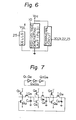
- Figure 6 shows the relationship between the source voltage V CC , the boosted source voltage V CC , the high--voltage generating unit 10, the cells 25, and the peripheral circuits 20, 21, 22, and 23.
- Figure 7 shows an embodiment of the ring oscillator 11 shown in Fig. 3.
- the ring oscillator in Fig. 7 is formed as a well-known ring oscillator having a three-stage negative inverter. That is, three pairs of transistors Q 11' Q 12 , Q 14 , Q 15 , and Q 17 , Q 18 form the negative inverter circuits.
- the transistors Q 11 , Q 14 , and Q 17 may be formed as depletion transistors, and the transistors Q 12 , Q 15 , and Q 18 may be formed as enhancement transistors.
- the transistors Q 13 ' Q 16 ' and Q 19 may be formed as depletion--type transistors or as enhancement-type transistors so as to form a resistor between the inverter stages.
- Capacitors C 11 , C 12 , and C 13 are used for delaying signal wave forms so that the output of the transistor Q 19 is fed back to the gate of the transistor Q 12 . These capacitors may be formed in the same manner as the capacitor C 1 shown in Fig. 3.
Landscapes
- Engineering & Computer Science (AREA)
- Microelectronics & Electronic Packaging (AREA)
- Computer Hardware Design (AREA)
- Power Engineering (AREA)
- Static Random-Access Memory (AREA)
- Dram (AREA)
- Semiconductor Memories (AREA)
- Power Sources (AREA)
Applications Claiming Priority (2)
| Application Number | Priority Date | Filing Date | Title |
|---|---|---|---|
| JP57043977A JPS58161195A (ja) | 1982-03-19 | 1982-03-19 | スタテイツク型半導体記憶装置 |
| JP43977/82 | 1982-03-19 |
Publications (2)
| Publication Number | Publication Date |
|---|---|
| EP0089836A2 true EP0089836A2 (de) | 1983-09-28 |
| EP0089836A3 EP0089836A3 (de) | 1985-12-04 |
Family
ID=12678771
Family Applications (1)
| Application Number | Title | Priority Date | Filing Date |
|---|---|---|---|
| EP83301539A Withdrawn EP0089836A3 (de) | 1982-03-19 | 1983-03-18 | Statische Halbleiterspeicheranordnung |
Country Status (2)
| Country | Link |
|---|---|
| EP (1) | EP0089836A3 (de) |
| JP (1) | JPS58161195A (de) |
Cited By (3)
| Publication number | Priority date | Publication date | Assignee | Title |
|---|---|---|---|---|
| EP0106222A3 (en) * | 1982-10-12 | 1986-01-22 | Kabushiki Kaisha Toshiba | Semiconductor memory device |
| DE3635344A1 (de) * | 1985-12-10 | 1987-06-11 | Mitsubishi Electric Corp | Wortzeilen-treiberschaltung |
| DE4037207A1 (de) * | 1990-09-19 | 1992-04-02 | Samsung Electronics Co Ltd | Stromeinstellschaltkreis fuer ein statisches ram |
Families Citing this family (1)
| Publication number | Priority date | Publication date | Assignee | Title |
|---|---|---|---|---|
| JP2003059273A (ja) | 2001-08-09 | 2003-02-28 | Hitachi Ltd | 半導体記憶装置 |
Family Cites Families (2)
| Publication number | Priority date | Publication date | Assignee | Title |
|---|---|---|---|---|
| JPS5570986A (en) * | 1978-11-24 | 1980-05-28 | Hitachi Ltd | Semiconductor intergrated circuit device |
| JPS5712481A (en) * | 1980-06-26 | 1982-01-22 | Mitsubishi Electric Corp | Semiconductor memory device |
-
1982
- 1982-03-19 JP JP57043977A patent/JPS58161195A/ja active Pending
-
1983
- 1983-03-18 EP EP83301539A patent/EP0089836A3/de not_active Withdrawn
Cited By (4)
| Publication number | Priority date | Publication date | Assignee | Title |
|---|---|---|---|---|
| EP0106222A3 (en) * | 1982-10-12 | 1986-01-22 | Kabushiki Kaisha Toshiba | Semiconductor memory device |
| DE3635344A1 (de) * | 1985-12-10 | 1987-06-11 | Mitsubishi Electric Corp | Wortzeilen-treiberschaltung |
| US4788664A (en) * | 1985-12-10 | 1988-11-29 | Mitsubishi Denki Kabushiki Kaisha | Word line drive circuit |
| DE4037207A1 (de) * | 1990-09-19 | 1992-04-02 | Samsung Electronics Co Ltd | Stromeinstellschaltkreis fuer ein statisches ram |
Also Published As
| Publication number | Publication date |
|---|---|
| JPS58161195A (ja) | 1983-09-24 |
| EP0089836A3 (de) | 1985-12-04 |
Similar Documents
| Publication | Publication Date | Title |
|---|---|---|
| US5600598A (en) | Memory cell and wordline driver for embedded DRAM in ASIC process | |
| US5010259A (en) | Voltage boosting circuit and operating method thereof | |
| EP0475407A2 (de) | DRAM mit einem Wortleitungsbetriebsschaltungssystem | |
| EP0100908A2 (de) | Halbleiterspeicheranordnung mit mehreren Ladungsspeichertypzellen | |
| US4532609A (en) | Semiconductor memory device | |
| EP0090632B1 (de) | Statische Randomspeicheranordnung | |
| US5051959A (en) | Complementary semiconductor memory device including cell access transistor and word line driving transistor having channels of different conductivity type | |
| US5886942A (en) | Word line driver and semiconductor device | |
| KR910007436B1 (ko) | 반도체 비휘발성 메모리 장치 | |
| US5132575A (en) | Method for providing multi-level potentials at a sense node | |
| KR0153847B1 (ko) | 반도체 기억장치 | |
| US4442481A (en) | Low power decoder circuit | |
| US4731552A (en) | Boost signal generator with bootstrap means | |
| EP0121798A2 (de) | Dynamische Halbleiterspeicheranordnung | |
| EP0073677B1 (de) | MIS Transistorschaltung mit einer Spannungshalteschaltung | |
| US5179535A (en) | Substrate bias voltage generating circuit including an internal frequency divider and driven by an externally applied clock signal | |
| EP0155117A2 (de) | Spannungsdetektor | |
| EP0089836A2 (de) | Statische Halbleiterspeicheranordnung | |
| US4496850A (en) | Semiconductor circuit for enabling a quick rise of the potential _on the word line for driving a clock signal line | |
| EP0055038B1 (de) | Steuerung einer Signalspannung für eine Halbleitervorrichtung | |
| EP0061271B1 (de) | Dynamische MOS-Speicheranordnung | |
| US4831589A (en) | EEPROM programming switch operable at low VCC | |
| EP0106222B1 (de) | Halbleiterspeicheranordnung | |
| EP0212946B1 (de) | Halbleiterspeicheranordnung | |
| US4833343A (en) | Clock generator having complementary transistors |
Legal Events
| Date | Code | Title | Description |
|---|---|---|---|
| PUAI | Public reference made under article 153(3) epc to a published international application that has entered the european phase |
Free format text: ORIGINAL CODE: 0009012 |
|
| AK | Designated contracting states |
Designated state(s): DE FR GB |
|
| PUAL | Search report despatched |
Free format text: ORIGINAL CODE: 0009013 |
|
| AK | Designated contracting states |
Designated state(s): DE FR GB |
|
| STAA | Information on the status of an ep patent application or granted ep patent |
Free format text: STATUS: THE APPLICATION IS DEEMED TO BE WITHDRAWN |
|
| 18D | Application deemed to be withdrawn |
Effective date: 19860805 |
|
| RIN1 | Information on inventor provided before grant (corrected) |
Inventor name: SEKI, TERUO Inventor name: AOYAMA, KEIZO Inventor name: YAMAUCHI, TAKAHIKO |