EP0090161A2 - Procédé de fabrication des cellules de ménoire dynamiques à accès aléatoires (RAM) selon la technologie à double grille en silicium polycrystallin - Google Patents
Procédé de fabrication des cellules de ménoire dynamiques à accès aléatoires (RAM) selon la technologie à double grille en silicium polycrystallin Download PDFInfo
- Publication number
- EP0090161A2 EP0090161A2 EP83101406A EP83101406A EP0090161A2 EP 0090161 A2 EP0090161 A2 EP 0090161A2 EP 83101406 A EP83101406 A EP 83101406A EP 83101406 A EP83101406 A EP 83101406A EP 0090161 A2 EP0090161 A2 EP 0090161A2
- Authority
- EP
- European Patent Office
- Prior art keywords
- oxide
- thick oxide
- region
- etching
- areas
- Prior art date
- Legal status (The legal status is an assumption and is not a legal conclusion. Google has not performed a legal analysis and makes no representation as to the accuracy of the status listed.)
- Granted
Links
Images
Classifications
-
- H—ELECTRICITY
- H10—SEMICONDUCTOR DEVICES; ELECTRIC SOLID-STATE DEVICES NOT OTHERWISE PROVIDED FOR
- H10P—GENERIC PROCESSES OR APPARATUS FOR THE MANUFACTURE OR TREATMENT OF DEVICES COVERED BY CLASS H10
- H10P30/00—Ion implantation into wafers, substrates or parts of devices
- H10P30/20—Ion implantation into wafers, substrates or parts of devices into semiconductor materials, e.g. for doping
- H10P30/202—Ion implantation into wafers, substrates or parts of devices into semiconductor materials, e.g. for doping characterised by the semiconductor materials
- H10P30/204—Ion implantation into wafers, substrates or parts of devices into semiconductor materials, e.g. for doping characterised by the semiconductor materials into Group IV semiconductors
-
- H—ELECTRICITY
- H10—SEMICONDUCTOR DEVICES; ELECTRIC SOLID-STATE DEVICES NOT OTHERWISE PROVIDED FOR
- H10B—ELECTRONIC MEMORY DEVICES
- H10B12/00—Dynamic random access memory [DRAM] devices
- H10B12/01—Manufacture or treatment
-
- H—ELECTRICITY
- H10—SEMICONDUCTOR DEVICES; ELECTRIC SOLID-STATE DEVICES NOT OTHERWISE PROVIDED FOR
- H10P—GENERIC PROCESSES OR APPARATUS FOR THE MANUFACTURE OR TREATMENT OF DEVICES COVERED BY CLASS H10
- H10P30/00—Ion implantation into wafers, substrates or parts of devices
- H10P30/20—Ion implantation into wafers, substrates or parts of devices into semiconductor materials, e.g. for doping
- H10P30/21—Ion implantation into wafers, substrates or parts of devices into semiconductor materials, e.g. for doping of electrically active species
- H10P30/212—Through-implantation
-
- H—ELECTRICITY
- H10—SEMICONDUCTOR DEVICES; ELECTRIC SOLID-STATE DEVICES NOT OTHERWISE PROVIDED FOR
- H10P—GENERIC PROCESSES OR APPARATUS FOR THE MANUFACTURE OR TREATMENT OF DEVICES COVERED BY CLASS H10
- H10P30/00—Ion implantation into wafers, substrates or parts of devices
- H10P30/20—Ion implantation into wafers, substrates or parts of devices into semiconductor materials, e.g. for doping
- H10P30/22—Ion implantation into wafers, substrates or parts of devices into semiconductor materials, e.g. for doping using masks
-
- H—ELECTRICITY
- H10—SEMICONDUCTOR DEVICES; ELECTRIC SOLID-STATE DEVICES NOT OTHERWISE PROVIDED FOR
- H10P—GENERIC PROCESSES OR APPARATUS FOR THE MANUFACTURE OR TREATMENT OF DEVICES COVERED BY CLASS H10
- H10P50/00—Etching of wafers, substrates or parts of devices
- H10P50/20—Dry etching; Plasma etching; Reactive-ion etching
- H10P50/28—Dry etching; Plasma etching; Reactive-ion etching of insulating materials
- H10P50/282—Dry etching; Plasma etching; Reactive-ion etching of insulating materials of inorganic materials
- H10P50/283—Dry etching; Plasma etching; Reactive-ion etching of insulating materials of inorganic materials by chemical means
-
- H—ELECTRICITY
- H10—SEMICONDUCTOR DEVICES; ELECTRIC SOLID-STATE DEVICES NOT OTHERWISE PROVIDED FOR
- H10P—GENERIC PROCESSES OR APPARATUS FOR THE MANUFACTURE OR TREATMENT OF DEVICES COVERED BY CLASS H10
- H10P76/00—Manufacture or treatment of masks on semiconductor bodies, e.g. by lithography or photolithography
- H10P76/40—Manufacture or treatment of masks on semiconductor bodies, e.g. by lithography or photolithography of masks comprising inorganic materials
-
- H—ELECTRICITY
- H10—SEMICONDUCTOR DEVICES; ELECTRIC SOLID-STATE DEVICES NOT OTHERWISE PROVIDED FOR
- H10W—GENERIC PACKAGES, INTERCONNECTIONS, CONNECTORS OR OTHER CONSTRUCTIONAL DETAILS OF DEVICES COVERED BY CLASS H10
- H10W10/00—Isolation regions in semiconductor bodies between components of integrated devices
- H10W10/01—Manufacture or treatment
- H10W10/011—Manufacture or treatment of isolation regions comprising dielectric materials
- H10W10/012—Manufacture or treatment of isolation regions comprising dielectric materials using local oxidation of silicon [LOCOS]
- H10W10/0125—Manufacture or treatment of isolation regions comprising dielectric materials using local oxidation of silicon [LOCOS] comprising introducing electrical impurities in local oxidation regions, e.g. to alter LOCOS oxide growth characteristics
- H10W10/0126—Manufacture or treatment of isolation regions comprising dielectric materials using local oxidation of silicon [LOCOS] comprising introducing electrical impurities in local oxidation regions, e.g. to alter LOCOS oxide growth characteristics introducing electrical active impurities in local oxidation regions to create channel stoppers
-
- H—ELECTRICITY
- H10—SEMICONDUCTOR DEVICES; ELECTRIC SOLID-STATE DEVICES NOT OTHERWISE PROVIDED FOR
- H10W—GENERIC PACKAGES, INTERCONNECTIONS, CONNECTORS OR OTHER CONSTRUCTIONAL DETAILS OF DEVICES COVERED BY CLASS H10
- H10W10/00—Isolation regions in semiconductor bodies between components of integrated devices
- H10W10/10—Isolation regions comprising dielectric materials
- H10W10/13—Isolation regions comprising dielectric materials formed using local oxidation of silicon [LOCOS], e.g. sealed interface localised oxidation [SILO] or side-wall mask isolation [SWAMI]
Definitions
- RAM random access memory
- the double polysilicon gate (Si 2 gate) process is to be regarded as the standard process for the implementation of dynamic RAM memories. Such a process for the manufacture of 16,384 bit dynamic random access memory is described in the IEEE Journal of Solid-State Circuits, Vol. Sc. 11, October 1976, pages 570 to 573.
- the minimum possible isolation distance of the LOCOS insulation is therefore twice the length of the bird's beak above the minimum structural dimension. It follows from this that in the case of the 256 K RAM memory cell known from the ISSCC 1980 volume, an additional space requirement of about 25% of the cell area is required. The higher space requirement for the insulation area leads to an increase in the total chip area. Another fundamental difficulty in reducing the insulation spacing arises from the so-called short channel effect of the thick oxide transistor. The thick oxide transistor loses its blocking capability for insulation distances of less than 2.5 / ⁇ m.
- HiC high capacity RAM cell concept
- the object on which the invention is based is now to produce dynamic RAM memory cells with double polysilicon gate technology in the direction of reducing the space requirement, simplifying the technological process and improving the electrical insulation between adjacent cells and thus increasing the dielectric strength.
- This object is achieved according to the invention by a method of the type mentioned at the outset in that the thickness of the oxide in the barrier region at the transitions between the thick oxide region and the thin oxide region is reduced both axially and laterally by etching using the photoresist mask provided for the arsenic and boron ion implantation , the photoresist edge being placed in the middle of the thick oxide region between the memory cell and thick oxide transistor.
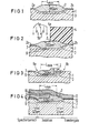
- FIGS. 1 to 4 illustrate the process flow according to an embodiment according to claim 2 in a sectional view.
- FIG. 1 shows a p-doped semiconductor body 1 (20 ohm.cm), on which the thick oxide layer 2 required for the separation of the active areas has been produced in a conventional manner using LOCOS technology.
- Boron doping has been introduced in a known manner under the thick oxide regions as a channel stop (setting the threshold voltage of about 1 volt), with boron ions having a dose of 2. 10 12 cm -2 and an energy of 120 keV before LOCOS oxidation using the nitride mask can be implanted on the active areas.
- the boron field implantation is designated by the reference number 3.
- the thick oxide layer 2 has a layer thickness of 650 nm, the thin oxide region 2a, 2b a layer thickness of 75 nm.
- the area of the minimum structural dimension List is shown above the sectional drawing.
- the storage areas are defined in which boron and arsenic ions 5a, 5b are implanted in the semiconductor body 1, the photoresist edge 4a being placed in the center of the insulation region (2, 2a, 2b).
- the oxide surface is then etched off, the thickness of the free thin oxide region 2a being reduced to 25 nm and the thickness of the free thick oxide region 2 being reduced to 600 nm.
- HiC implantation high capacity now takes place, with a lower-lying boron implantation 5a and then a flat arsenic implantation 5b being introduced into the storage area.
- the implantation parameters of the boron implantation 5a are selected so that both a maximum gain in the storage capacity and a sufficiently good dielectric strength of the storage diode is ensured, and the implantation is introduced sufficiently deep so that as much of the boron dose as possible covers the exposed thick oxide area 2 penetrates and increases the doping of the channel stop (3).
- the implantation dose is set to 7 ⁇ 10 12 Bcm -2 at an energy of 140 keV.
- the subsequent arsenic implantation 5b is used to set the threshold voltage in the storage area. Because of the low penetration depth (energy 100 keV, 1 x 10 14 Ascm -2 ), the arsenic cannot penetrate the thick oxide area 2.
- the implanted boron region is designated by reference number 6, the implanted arsenic region by 7.
- FIG. 3 In the next process step, the exposed thick and thin oxide areas (2, 2a) are overetched by 150 nm, whereby the bird's beak length (see arrow 8) is reduced to about 0.3 ⁇ m.
- the photoresist mask 4 is removed and a full overetch of the surface by 100 nm is connected.
- the bird's beak 8a of the storage area is reduced to approximately 0.25 ⁇ m at 350 nm field oxide thickness. For a typical 256 K cell design, this corresponds to a gain of 25 in the memory area.
- the bird's beak (8b) of the rest active areas is about 0.5 / ⁇ m.
- the insulation behavior of the thinned field oxide area (2) is significantly better than that of the undiluted areas (prior art) because of the increased boron doping.
- a gain in the reverse voltage of more than 10 V is achieved by the method according to the invention.
- FIG. 4 shows the arrangement after carrying out the gate oxidation (12), applying and structuring the polysilicon 1 electrode 9, producing the insulation oxide 10 and applying / structuring the polysilicon 2 electrode 11.
- FIG. 4 also shows the minimum structural dimensions L min and the length of the bird's beak L V.
- the active memory area of the cell, the area of a selection transistor and the isolation area are also marked in FIG. 4 by double or directional arrows.
- wet-chemical etching processes e.g. buffered hydrofluoric acid solutions
- reactive dry etching processes such as preferably the plasma etching process
- the entire overetching step can be carried out using the photoresist mask 4 (for the ion implantations) with 200 nm removal of the thick oxide transistor before the ion implantation (5a, 5b).
- the boron / arsenic ion implantation. is then introduced in the following step without scatter oxide, the energy of the boron ion implantation being reduced accordingly.
Landscapes
- Engineering & Computer Science (AREA)
- Manufacturing & Machinery (AREA)
- Semiconductor Memories (AREA)
- Element Separation (AREA)
Priority Applications (1)
| Application Number | Priority Date | Filing Date | Title |
|---|---|---|---|
| AT83101406T ATE23413T1 (de) | 1982-02-18 | 1983-02-14 | Verfahren zum herstellen von dynamischen halbleiter-speicherzellen mit wahlfreiem zugriff (ram) nach der doppel-polysilizium-gate- technologie. |
Applications Claiming Priority (2)
| Application Number | Priority Date | Filing Date | Title |
|---|---|---|---|
| DE3205858 | 1982-02-18 | ||
| DE19823205858 DE3205858A1 (de) | 1982-02-18 | 1982-02-18 | Verfahren zum herstellen von dynamischen halbleiter-speicherzellen mit wahlfreiem zugriff (ram) nach der doppel-polysilizium-gate-technologie |
Publications (3)
| Publication Number | Publication Date |
|---|---|
| EP0090161A2 true EP0090161A2 (fr) | 1983-10-05 |
| EP0090161A3 EP0090161A3 (en) | 1984-05-16 |
| EP0090161B1 EP0090161B1 (fr) | 1986-11-05 |
Family
ID=6156096
Family Applications (1)
| Application Number | Title | Priority Date | Filing Date |
|---|---|---|---|
| EP83101406A Expired EP0090161B1 (fr) | 1982-02-18 | 1983-02-14 | Procédé de fabrication des cellules de ménoire dynamiques à accès aléatoires (RAM) selon la technologie à double grille en silicium polycrystallin |
Country Status (5)
| Country | Link |
|---|---|
| US (1) | US4414058A (fr) |
| EP (1) | EP0090161B1 (fr) |
| JP (1) | JPS58153363A (fr) |
| AT (1) | ATE23413T1 (fr) |
| DE (2) | DE3205858A1 (fr) |
Cited By (1)
| Publication number | Priority date | Publication date | Assignee | Title |
|---|---|---|---|---|
| EP0209939A1 (fr) * | 1985-07-11 | 1987-01-28 | Koninklijke Philips Electronics N.V. | Procédé de fabrication d'un dispositif semi-conducteur |
Families Citing this family (11)
| Publication number | Priority date | Publication date | Assignee | Title |
|---|---|---|---|---|
| US4536947A (en) * | 1983-07-14 | 1985-08-27 | Intel Corporation | CMOS process for fabricating integrated circuits, particularly dynamic memory cells with storage capacitors |
| JPS60106142A (ja) * | 1983-11-15 | 1985-06-11 | Nec Corp | 半導体素子の製造方法 |
| US4570331A (en) * | 1984-01-26 | 1986-02-18 | Inmos Corporation | Thick oxide field-shield CMOS process |
| US4707457A (en) * | 1986-04-03 | 1987-11-17 | Advanced Micro Devices, Inc. | Method for making improved contact for integrated circuit structure |
| JP2886183B2 (ja) * | 1988-06-28 | 1999-04-26 | 三菱電機株式会社 | フィールド分離絶縁膜の製造方法 |
| US5234859A (en) * | 1988-06-28 | 1993-08-10 | Mitsubishi Denki Kabushiki Kaisha | LOCOS type field isolating film and semiconductor memory device formed therewith |
| WO1990005377A1 (fr) * | 1988-10-31 | 1990-05-17 | Micron Technology, Inc. | Reduction localisee de l'invasion par l'oxyde de champ |
| US4959325A (en) * | 1989-02-24 | 1990-09-25 | Micron Technology, Inc. | Reduction of electric field effect in the bird's beak region of a DRAM cell following expansion of active region through local encroachment reduction |
| CA2051686C (fr) * | 1990-01-22 | 2001-10-23 | Bing Yeh | Memoire monotransistor a remanence a contenu modifiable electriquement a grille flottante recristallisee |
| US5332682A (en) * | 1990-08-31 | 1994-07-26 | Micron Semiconductor, Inc. | Local encroachment reduction |
| US6767794B2 (en) * | 1998-01-05 | 2004-07-27 | Advanced Micro Devices, Inc. | Method of making ultra thin oxide formation using selective etchback technique integrated with thin nitride layer for high performance MOSFET |
Family Cites Families (5)
| Publication number | Priority date | Publication date | Assignee | Title |
|---|---|---|---|---|
| US4075045A (en) * | 1976-02-09 | 1978-02-21 | International Business Machines Corporation | Method for fabricating FET one-device memory cells with two layers of polycrystalline silicon and fabrication of integrated circuits containing arrays of the memory cells charge storage capacitors utilizing five basic pattern deliberating steps |
| US4112575A (en) * | 1976-12-20 | 1978-09-12 | Texas Instruments Incorporated | Fabrication methods for the high capacity ram cell |
| US4145803A (en) * | 1977-07-22 | 1979-03-27 | Texas Instruments Incorporated | Lithographic offset alignment techniques for RAM fabrication |
| DE2902665A1 (de) * | 1979-01-24 | 1980-08-07 | Siemens Ag | Verfahren zum herstellen von integrierten mos-schaltungen in silizium-gate- technologie |
| US4335502A (en) * | 1980-10-01 | 1982-06-22 | Standard Microsystems Corporation | Method for manufacturing metal-oxide silicon devices |
-
1982
- 1982-02-18 DE DE19823205858 patent/DE3205858A1/de not_active Withdrawn
- 1982-12-13 US US06/449,145 patent/US4414058A/en not_active Expired - Fee Related
-
1983
- 1983-02-14 EP EP83101406A patent/EP0090161B1/fr not_active Expired
- 1983-02-14 AT AT83101406T patent/ATE23413T1/de not_active IP Right Cessation
- 1983-02-14 DE DE8383101406T patent/DE3367484D1/de not_active Expired
- 1983-02-17 JP JP58025462A patent/JPS58153363A/ja active Pending
Cited By (1)
| Publication number | Priority date | Publication date | Assignee | Title |
|---|---|---|---|---|
| EP0209939A1 (fr) * | 1985-07-11 | 1987-01-28 | Koninklijke Philips Electronics N.V. | Procédé de fabrication d'un dispositif semi-conducteur |
Also Published As
| Publication number | Publication date |
|---|---|
| ATE23413T1 (de) | 1986-11-15 |
| EP0090161B1 (fr) | 1986-11-05 |
| EP0090161A3 (en) | 1984-05-16 |
| DE3205858A1 (de) | 1983-08-25 |
| DE3367484D1 (en) | 1986-12-11 |
| JPS58153363A (ja) | 1983-09-12 |
| US4414058A (en) | 1983-11-08 |
Similar Documents
| Publication | Publication Date | Title |
|---|---|---|
| DE3844388C2 (fr) | ||
| EP0002670B1 (fr) | Procédé pour la fabrication d'un transistor bipolaire dans un substrat semi-conducteur | |
| DE3916228C2 (de) | Halbleiterspeichervorrichtung mit Stapelkondensatorzellenstruktur und Verfahren zu ihrer Herstellung | |
| EP0018501B1 (fr) | Procédé de fabrication de transistors â effet de champ verticaux à haute densité et matrice de cellules fabriquée selon ce procédé | |
| DE69329376T2 (de) | Verfahren zur Herstellung einer SOI-Transistor-DRAM | |
| DE69221530T2 (de) | Verfahren zum Erhöhen der Kapazität eines DRAMs durch Anodisieren der Polysiliziumschicht einer unteren Kondensatorplatte | |
| DE4201004C2 (de) | Verfahren zur Bildung eines Kondensators | |
| DE3780369T2 (de) | Verfahren zum herstellen einer halbleiterstruktur. | |
| DE3880750T2 (de) | Vertikale Transistor-/Kapazitätspeicherzellen-Struktur und Herstellungsverfahren dafür. | |
| DE4136420C2 (de) | Verfahren zur Bildung eines Kondensators | |
| DE3012363C2 (de) | Verfahren zur Bildung der Kanalbereiche und der Wannen von Halbleiterbauelementen | |
| DE2756855A1 (de) | Verfahren zum herstellen einer matrix aus speicherzellen mit hoher speicherkapazitaet | |
| DE2809233A1 (de) | Halbleitervorrichtung und verfahren zu ihrer herstellung | |
| DE4301690A1 (fr) | ||
| DE3029125A1 (de) | Halbleiterspeicher | |
| DE2928923C2 (fr) | ||
| DE4229363A1 (de) | Verfahren zur bildung eines kondensators | |
| DE2741152A1 (de) | Speicherzelle fuer einen silizium- gate-n-kanal-mos-direktzugriffspeicher und verfahren zu ihrer herstellung | |
| DE3787687T2 (de) | Halbleiterspeicher. | |
| DE4028488A1 (de) | Halbleiterspeichervorrichtung und verfahren zu ihrer herstellung | |
| DE2716691A1 (de) | Feldeffekttransistor und verfahren zu dessen herstellung | |
| EP0090161B1 (fr) | Procédé de fabrication des cellules de ménoire dynamiques à accès aléatoires (RAM) selon la technologie à double grille en silicium polycrystallin | |
| DE69132998T2 (de) | Speicheranordnung mit wahlfreiem Zugriff und Herstellungsverfahren dafür | |
| DE3788120T2 (de) | Verfahren zur herstellung gestapelter mos-strukturen. | |
| DE69028245T2 (de) | Dynamische RAM-Zelle mit hoher Dichte |
Legal Events
| Date | Code | Title | Description |
|---|---|---|---|
| PUAI | Public reference made under article 153(3) epc to a published international application that has entered the european phase |
Free format text: ORIGINAL CODE: 0009012 |
|
| AK | Designated contracting states |
Designated state(s): AT DE FR GB IT |
|
| PUAL | Search report despatched |
Free format text: ORIGINAL CODE: 0009013 |
|
| AK | Designated contracting states |
Designated state(s): AT DE FR GB IT |
|
| 17P | Request for examination filed |
Effective date: 19840528 |
|
| 17Q | First examination report despatched |
Effective date: 19860121 |
|
| GRAA | (expected) grant |
Free format text: ORIGINAL CODE: 0009210 |
|
| AK | Designated contracting states |
Kind code of ref document: B1 Designated state(s): AT DE FR GB IT |
|
| REF | Corresponds to: |
Ref document number: 23413 Country of ref document: AT Date of ref document: 19861115 Kind code of ref document: T |
|
| REF | Corresponds to: |
Ref document number: 3367484 Country of ref document: DE Date of ref document: 19861211 |
|
| ET | Fr: translation filed | ||
| PGFP | Annual fee paid to national office [announced via postgrant information from national office to epo] |
Ref country code: AT Payment date: 19870128 Year of fee payment: 5 |
|
| ITF | It: translation for a ep patent filed | ||
| PLBE | No opposition filed within time limit |
Free format text: ORIGINAL CODE: 0009261 |
|
| STAA | Information on the status of an ep patent application or granted ep patent |
Free format text: STATUS: NO OPPOSITION FILED WITHIN TIME LIMIT |
|
| 26N | No opposition filed | ||
| PG25 | Lapsed in a contracting state [announced via postgrant information from national office to epo] |
Ref country code: GB Effective date: 19890214 Ref country code: AT Effective date: 19890214 |
|
| GBPC | Gb: european patent ceased through non-payment of renewal fee | ||
| PG25 | Lapsed in a contracting state [announced via postgrant information from national office to epo] |
Ref country code: FR Free format text: LAPSE BECAUSE OF NON-PAYMENT OF DUE FEES Effective date: 19891027 |
|
| PG25 | Lapsed in a contracting state [announced via postgrant information from national office to epo] |
Ref country code: DE Effective date: 19891101 |
|
| REG | Reference to a national code |
Ref country code: FR Ref legal event code: ST |