EP0090193A2 - Spannungsvervielfachervorrichtung für Hochspannungsanlage, besonders für Anwendungen in der Raumfahrt. - Google Patents
Spannungsvervielfachervorrichtung für Hochspannungsanlage, besonders für Anwendungen in der Raumfahrt. Download PDFInfo
- Publication number
- EP0090193A2 EP0090193A2 EP83102081A EP83102081A EP0090193A2 EP 0090193 A2 EP0090193 A2 EP 0090193A2 EP 83102081 A EP83102081 A EP 83102081A EP 83102081 A EP83102081 A EP 83102081A EP 0090193 A2 EP0090193 A2 EP 0090193A2
- Authority
- EP
- European Patent Office
- Prior art keywords
- voltage multiplier
- section
- circuit components
- voltage
- electric field
- Prior art date
- Legal status (The legal status is an assumption and is not a legal conclusion. Google has not performed a legal analysis and makes no representation as to the accuracy of the status listed.)
- Granted
Links
- 230000005684 electric field Effects 0.000 claims abstract description 10
- 239000003990 capacitor Substances 0.000 claims description 7
- 239000002184 metal Substances 0.000 claims description 7
- 238000009413 insulation Methods 0.000 claims description 5
- 238000009826 distribution Methods 0.000 claims description 4
- 229920005749 polyurethane resin Polymers 0.000 claims description 4
- 229920005989 resin Polymers 0.000 claims description 3
- 239000011347 resin Substances 0.000 claims description 3
- 238000005266 casting Methods 0.000 claims description 2
- 238000004519 manufacturing process Methods 0.000 claims description 2
- 238000003466 welding Methods 0.000 claims description 2
- 239000007788 liquid Substances 0.000 claims 1
- 230000001066 destructive effect Effects 0.000 description 3
- 230000015572 biosynthetic process Effects 0.000 description 2
- 238000000034 method Methods 0.000 description 2
- 238000007599 discharging Methods 0.000 description 1
- 230000000694 effects Effects 0.000 description 1
- 230000008676 import Effects 0.000 description 1
- 239000000463 material Substances 0.000 description 1
- 238000012986 modification Methods 0.000 description 1
- 230000004048 modification Effects 0.000 description 1
- 238000005457 optimization Methods 0.000 description 1
- 238000005549 size reduction Methods 0.000 description 1
- 230000003313 weakening effect Effects 0.000 description 1
Images


Classifications
-
- H—ELECTRICITY
- H05—ELECTRIC TECHNIQUES NOT OTHERWISE PROVIDED FOR
- H05K—PRINTED CIRCUITS; CASINGS OR CONSTRUCTIONAL DETAILS OF ELECTRIC APPARATUS; MANUFACTURE OF ASSEMBLAGES OF ELECTRICAL COMPONENTS
- H05K9/00—Screening of apparatus or components against electric or magnetic fields
- H05K9/0007—Casings
- H05K9/002—Casings with localised screening
- H05K9/0039—Galvanic coupling of ground layer on printed circuit board [PCB] to conductive casing
Definitions
- This invention relates to a voltage multiplier device for high tension equipment, in particular for spatial applications.
- a further object of the invention is to provide a voltage multiplier, wherein the likelihood of partial or destructive discharges occurring is minimized, thereby improving the apparatus durability.
- Another object of this invention is to provide a voltage multiplier as indicated, which features good insulation, both outside and inside between the individual components thereof.
- a voltage multiplier device for high tension equipment in particular for spatial applications, according to the invention, comprising a first section including such circuit components as resistors, capacitors, and diodes operatively and function-wise interconnected together and being carried on a common mounting base, said first section being adapted to supply a high voltage, and a second driving section, and characterized in that electrostatic screens external to said first section are provided for controlling the present electric field, and in that it comprises a means of optimizing the potential gradient present between the components making up said first section.
- Said device 1 comprises two sections, of which a first section, designated with the reference numeral 2, constitutes the voltage multiplier proper, and a second section, designated with the reference numeral 3, constitutes the drive section of the final stage or voltage multiplier.
- the voltage multiplier 2 is divided, in turn, into a first element 2a and second element 2b, forming a multiplier by twelve and multiplier by thirty six, respectively.
- both the element 2a and element 2b of this invention are completely enclosed by a screen 14 formed from a wire mesh which is grounded.
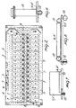
- FIG 2 illustrates schematically the multiplier by thirty six.
- Said multiplier comprises a base 4 having holes 5 (represented as thin line circles). Thick line circles represent the weld points 6 for assembling the components.
- Mounted on the base 4 are capacitors 7 (welded in the way shown in Figure 7), diodes 8 ( Figure 10), and a resistor 9 (Figure 8).
- Figure 3 shows a side view of the multiplier 36 of Figure 2, where the capacitors 7, diodes 8, and output cable 10 for the 36 kVolt high tension (welded as shown in Figure 9) may be seen.
- Figure 4 illustrates the multiplier-by-twelve element which, similarly to the multiplier-by-thirty six element shown in Figure 2, comprises a base 4' having holes 5' and weld points 6'. Welded to the base 4' are capacitors 7', diodes 8', resistors 9', resistors 11 (welded as shown in Figure 11), and a component 12 (assembled as shown in Figure 12).
- Figure 5 is a side view of the multiplier by twelve according to Figure 4. Said side view shows the capacitors 7', output cable 13 for the 12 kVolt high tension, and output cable 10' for the 36 kVolt high tension.
- Figures 6-12 illustrate the welding of the components and high tension cables, whereby a reduction in the applied electric field can be achieved, i.e. the optimization of the potential gradient.
- metal surfaces of various sizes such as balls or small cylinders 15, are provided. The dimensions of the metal surfaces 15 must be carefully determined, as is obvious to a person skilled in the art, to each time provide the best distribution.
- the method for manufacturing the voltage multiplier device of this invention is also of essential import and advantageous per se.
- bases are press formed with holes, onto which bases the components are then assembled while inserting at the same time the metal balls or cylinders 15. Thereafter, the thusly assembled bases are placed within electrostatic screens, wherefrom air is drawn out prior to casting the insulating polyurethane resins.
- the insulating polyurethane resins are cast, according to the invention, under a vacuum, in order to prevent the formation of air bubbles within the insulating dielectric which would represent weakening areas. In fact, there would otherwise be generated at said bubbles high potential differences, with attendant increased likelihood of destructive discharges taking place.
- the invention fully achieves its objects.
- the voltage multiplier device is highly reliable, by virtue of metal surfaces being inserted therein which afford an improved distribution of the potential existing between the components, with attendant reduction of the electric field where the tension is highest.
- a control of the electric field has been provided in the form of screens which completely enclose the voltage multiplier section and are grounded electrically.
- screens may be formed from wire mesh, thereby facilitating adhesion of the screen onto the insulating resins, and reducing the likelihood of air bubbles highly susceptible to discharging being formed between the screen and external surface of the dielectric.
- the insulating resins are cast under a vacuum to prevent the formation of air bubbles within the dielectric.
- the materials, as well as shapes and dimensions may be any ones meeting individual application requirements.
Landscapes
- Engineering & Computer Science (AREA)
- Microelectronics & Electronic Packaging (AREA)
- Electrostatic Separation (AREA)
- Rectifiers (AREA)
- Organic Insulating Materials (AREA)
Applications Claiming Priority (2)
| Application Number | Priority Date | Filing Date | Title |
|---|---|---|---|
| IT2048182 | 1982-03-30 | ||
| IT8220481A IT1151379B (it) | 1982-03-30 | 1982-03-30 | Dispositivo moltiplicatore di tensione per apparecchi ad alta tensione,in particolare per applicazioni spaziali |
Publications (3)
| Publication Number | Publication Date |
|---|---|
| EP0090193A2 true EP0090193A2 (de) | 1983-10-05 |
| EP0090193A3 EP0090193A3 (en) | 1984-02-15 |
| EP0090193B1 EP0090193B1 (de) | 1987-07-08 |
Family
ID=11167589
Family Applications (1)
| Application Number | Title | Priority Date | Filing Date |
|---|---|---|---|
| EP83102081A Expired EP0090193B1 (de) | 1982-03-30 | 1983-03-03 | Spannungsvervielfachervorrichtung für Hochspannungsanlage, besonders für Anwendungen in der Raumfahrt. |
Country Status (5)
| Country | Link |
|---|---|
| EP (1) | EP0090193B1 (de) |
| DE (1) | DE3372434D1 (de) |
| DK (1) | DK89483A (de) |
| ES (1) | ES520795A0 (de) |
| IT (1) | IT1151379B (de) |
Cited By (1)
| Publication number | Priority date | Publication date | Assignee | Title |
|---|---|---|---|---|
| EP0389976A3 (de) * | 1989-03-27 | 1992-08-26 | Matsushita Electric Industrial Co., Ltd. | Vorrichtung für eine Leistungs-Hochspannungsquelle |
Family Cites Families (4)
| Publication number | Priority date | Publication date | Assignee | Title |
|---|---|---|---|---|
| GB918834A (en) * | 1960-11-28 | 1963-02-20 | Westinghouse Electric Corp | High voltage rectifier apparatus |
| US3721746A (en) * | 1971-10-01 | 1973-03-20 | Motorola Inc | Shielding techniques for r.f. circuitry |
| GB1414625A (en) * | 1972-02-28 | 1975-11-19 | American Plasticraft Co | Insulation of electrical multiplier assemblies |
| FR2475792A1 (fr) * | 1980-02-12 | 1981-08-14 | Thomson Csf | Multiplicateur de tension integre |
-
1982
- 1982-03-30 IT IT8220481A patent/IT1151379B/it active
-
1983
- 1983-02-25 DK DK89483A patent/DK89483A/da not_active Application Discontinuation
- 1983-03-03 EP EP83102081A patent/EP0090193B1/de not_active Expired
- 1983-03-03 DE DE8383102081T patent/DE3372434D1/de not_active Expired
- 1983-03-21 ES ES520795A patent/ES520795A0/es active Granted
Cited By (1)
| Publication number | Priority date | Publication date | Assignee | Title |
|---|---|---|---|---|
| EP0389976A3 (de) * | 1989-03-27 | 1992-08-26 | Matsushita Electric Industrial Co., Ltd. | Vorrichtung für eine Leistungs-Hochspannungsquelle |
Also Published As
| Publication number | Publication date |
|---|---|
| IT8220481A0 (it) | 1982-03-30 |
| ES8402990A1 (es) | 1984-03-16 |
| DK89483A (da) | 1983-10-01 |
| DK89483D0 (da) | 1983-02-25 |
| DE3372434D1 (en) | 1987-08-13 |
| IT1151379B (it) | 1986-12-17 |
| EP0090193B1 (de) | 1987-07-08 |
| ES520795A0 (es) | 1984-03-16 |
| EP0090193A3 (en) | 1984-02-15 |
Similar Documents
| Publication | Publication Date | Title |
|---|---|---|
| US3816911A (en) | Shielding techniques for r.f. circuitry | |
| AU667974B2 (en) | Electrically balanced connector assembly | |
| EP0717390A2 (de) | Anzeigegerät mit einer Referenzpotential-Verdichtung | |
| US4783906A (en) | Method of making a customizable electrical article | |
| JPH04352305A (ja) | 三層構造スパイラルインダクタのインダクタンスの調整方法 | |
| US5113316A (en) | System for the assembly and connection of electronic circuit boards, particularly for use in motor vehicles | |
| DE69934659T2 (de) | Anordnung zum Zünden einer Entladungslampe und Herstellungsverfahren dafür | |
| EP0090193A2 (de) | Spannungsvervielfachervorrichtung für Hochspannungsanlage, besonders für Anwendungen in der Raumfahrt. | |
| DE19616195C2 (de) | Zündvorrichtung für einen Verbrennungsmotor | |
| EP0483820B1 (de) | Kopplungsstruktur für einen dielektrischen Filter | |
| DE4121449A1 (de) | Hoergeraet, insbesondere am kopf tragbares mini-hoergeraet, und verfahren zur herstellung | |
| DE8715073U1 (de) | Elektronische Baueinheit zur Steuerung von Funktionen eines Kraftfahrzeugs | |
| DE3464295D1 (en) | Electric discharge tube and method of manufacturing an electrically conductive layer on a wall portion of the envelope of such a tube | |
| US20060061944A1 (en) | Plasma display device | |
| DE19508625C1 (de) | Ableitung elektrostatischer Aufladungen an einem elektrisch isoliert gelagerten Drosselklappenstutzen einer Brennkraftmaschine | |
| JP3730137B2 (ja) | 電力変換装置 | |
| US4195278A (en) | High voltage terminal structure and flyback transformer | |
| JPH10215038A (ja) | 複合型回路基板 | |
| DE3436842C2 (de) | ||
| KR20010075399A (ko) | 집적화된 전자총 및 전자 모듈 | |
| DE4329991A1 (de) | Kopfhörer mit elektrostatischem Gegentaktwandler | |
| JP3203267B2 (ja) | イオン加速装置 | |
| EP1081996A2 (de) | Elektromagnetische Abschirmung für einen Kabelschacht und elektronisches Gerät mit einem Kabelschacht | |
| JPH05102671A (ja) | 電子回路基板 | |
| EP0136568A3 (de) | Elektrisches Gerät |
Legal Events
| Date | Code | Title | Description |
|---|---|---|---|
| PUAI | Public reference made under article 153(3) epc to a published international application that has entered the european phase |
Free format text: ORIGINAL CODE: 0009012 |
|
| AK | Designated contracting states |
Designated state(s): BE DE FR GB NL SE |
|
| PUAL | Search report despatched |
Free format text: ORIGINAL CODE: 0009013 |
|
| AK | Designated contracting states |
Designated state(s): BE DE FR GB NL SE |
|
| 17P | Request for examination filed |
Effective date: 19840802 |
|
| 17Q | First examination report despatched |
Effective date: 19860319 |
|
| GRAA | (expected) grant |
Free format text: ORIGINAL CODE: 0009210 |
|
| AK | Designated contracting states |
Kind code of ref document: B1 Designated state(s): BE DE FR GB NL SE |
|
| PG25 | Lapsed in a contracting state [announced via postgrant information from national office to epo] |
Ref country code: NL Effective date: 19870708 Ref country code: FR Free format text: THE PATENT HAS BEEN ANNULLED BY A DECISION OF A NATIONAL AUTHORITY Effective date: 19870708 Ref country code: BE Effective date: 19870708 |
|
| PG25 | Lapsed in a contracting state [announced via postgrant information from national office to epo] |
Ref country code: SE Effective date: 19870731 |
|
| REF | Corresponds to: |
Ref document number: 3372434 Country of ref document: DE Date of ref document: 19870813 |
|
| EN | Fr: translation not filed | ||
| NLV1 | Nl: lapsed or annulled due to failure to fulfill the requirements of art. 29p and 29m of the patents act | ||
| PLBE | No opposition filed within time limit |
Free format text: ORIGINAL CODE: 0009261 |
|
| STAA | Information on the status of an ep patent application or granted ep patent |
Free format text: STATUS: NO OPPOSITION FILED WITHIN TIME LIMIT |
|
| 26N | No opposition filed | ||
| GBPC | Gb: european patent ceased through non-payment of renewal fee | ||
| PG25 | Lapsed in a contracting state [announced via postgrant information from national office to epo] |
Ref country code: GB Free format text: LAPSE BECAUSE OF NON-PAYMENT OF DUE FEES Effective date: 19881122 |
|
| PG25 | Lapsed in a contracting state [announced via postgrant information from national office to epo] |
Ref country code: DE Effective date: 19881201 |