EP0090220B1 - Circuit "squid" supraconductif - Google Patents
Circuit "squid" supraconductif Download PDFInfo
- Publication number
- EP0090220B1 EP0090220B1 EP83102355A EP83102355A EP0090220B1 EP 0090220 B1 EP0090220 B1 EP 0090220B1 EP 83102355 A EP83102355 A EP 83102355A EP 83102355 A EP83102355 A EP 83102355A EP 0090220 B1 EP0090220 B1 EP 0090220B1
- Authority
- EP
- European Patent Office
- Prior art keywords
- squid
- stage
- current
- input
- circuit
- Prior art date
- Legal status (The legal status is an assumption and is not a legal conclusion. Google has not performed a legal analysis and makes no representation as to the accuracy of the status listed.)
- Expired
Links
- 241000238366 Cephalopoda Species 0.000 title claims description 141
- 230000008878 coupling Effects 0.000 claims description 22
- 238000010168 coupling process Methods 0.000 claims description 22
- 238000005859 coupling reaction Methods 0.000 claims description 22
- 230000010355 oscillation Effects 0.000 claims description 9
- 230000005540 biological transmission Effects 0.000 claims description 5
- 230000004907 flux Effects 0.000 description 19
- 230000005291 magnetic effect Effects 0.000 description 16
- 230000004044 response Effects 0.000 description 9
- 230000035945 sensitivity Effects 0.000 description 8
- 238000010586 diagram Methods 0.000 description 6
- 230000001965 increasing effect Effects 0.000 description 5
- 238000000034 method Methods 0.000 description 5
- 238000004088 simulation Methods 0.000 description 4
- 230000005428 wave function Effects 0.000 description 4
- 230000008901 benefit Effects 0.000 description 3
- 239000003990 capacitor Substances 0.000 description 3
- 238000001514 detection method Methods 0.000 description 3
- 230000003993 interaction Effects 0.000 description 3
- 230000004888 barrier function Effects 0.000 description 2
- 238000005516 engineering process Methods 0.000 description 2
- 239000002887 superconductor Substances 0.000 description 2
- 235000019892 Stellar Nutrition 0.000 description 1
- 230000002411 adverse Effects 0.000 description 1
- 230000008859 change Effects 0.000 description 1
- 238000005094 computer simulation Methods 0.000 description 1
- 230000001419 dependent effect Effects 0.000 description 1
- 230000000694 effects Effects 0.000 description 1
- 230000002708 enhancing effect Effects 0.000 description 1
- 230000001747 exhibiting effect Effects 0.000 description 1
- 239000011810 insulating material Substances 0.000 description 1
- 230000008569 process Effects 0.000 description 1
- 230000001629 suppression Effects 0.000 description 1
- 230000007704 transition Effects 0.000 description 1
Images





Classifications
-
- G—PHYSICS
- G01—MEASURING; TESTING
- G01R—MEASURING ELECTRIC VARIABLES; MEASURING MAGNETIC VARIABLES
- G01R33/00—Arrangements or instruments for measuring magnetic variables
- G01R33/02—Measuring direction or magnitude of magnetic fields or magnetic flux
- G01R33/035—Measuring direction or magnitude of magnetic fields or magnetic flux using superconductive devices
- G01R33/0354—SQUIDS
-
- H—ELECTRICITY
- H03—ELECTRONIC CIRCUITRY
- H03H—IMPEDANCE NETWORKS, e.g. RESONANT CIRCUITS; RESONATORS
- H03H7/00—Multiple-port networks comprising only passive electrical elements as network components
- H03H7/38—Impedance-matching networks
-
- Y—GENERAL TAGGING OF NEW TECHNOLOGICAL DEVELOPMENTS; GENERAL TAGGING OF CROSS-SECTIONAL TECHNOLOGIES SPANNING OVER SEVERAL SECTIONS OF THE IPC; TECHNICAL SUBJECTS COVERED BY FORMER USPC CROSS-REFERENCE ART COLLECTIONS [XRACs] AND DIGESTS
- Y10—TECHNICAL SUBJECTS COVERED BY FORMER USPC
- Y10S—TECHNICAL SUBJECTS COVERED BY FORMER USPC CROSS-REFERENCE ART COLLECTIONS [XRACs] AND DIGESTS
- Y10S505/00—Superconductor technology: apparatus, material, process
- Y10S505/825—Apparatus per se, device per se, or process of making or operating same
- Y10S505/856—Electrical transmission or interconnection system
- Y10S505/857—Nonlinear solid-state device system or circuit
- Y10S505/858—Digital logic
-
- Y—GENERAL TAGGING OF NEW TECHNOLOGICAL DEVELOPMENTS; GENERAL TAGGING OF CROSS-SECTIONAL TECHNOLOGIES SPANNING OVER SEVERAL SECTIONS OF THE IPC; TECHNICAL SUBJECTS COVERED BY FORMER USPC CROSS-REFERENCE ART COLLECTIONS [XRACs] AND DIGESTS
- Y10—TECHNICAL SUBJECTS COVERED BY FORMER USPC
- Y10S—TECHNICAL SUBJECTS COVERED BY FORMER USPC CROSS-REFERENCE ART COLLECTIONS [XRACs] AND DIGESTS
- Y10S505/00—Superconductor technology: apparatus, material, process
- Y10S505/825—Apparatus per se, device per se, or process of making or operating same
- Y10S505/856—Electrical transmission or interconnection system
- Y10S505/857—Nonlinear solid-state device system or circuit
- Y10S505/865—Nonlinear solid-state device system or circuit with josephson junction
Definitions
- This invention relates to a SQUID circuit (Superconducting Quantum Interference Devices), and more particularly to a circuit comprising at least two cascaded DC SQUID stages the first stage including a superconducting loop with two series connected Josephson devices shunted with resistors to render the devices non-hysteretic, terminals for providing a DC bias current to the loop, input means for applying input signals to the SQUID, and an output terminal for delivering output currents to the second SQUID stage.
- SQUID circuit Superconducting Quantum Interference Devices
- Both RF and DC SQUID's are known in the art, and have been proposed for use in volt meters, current meters, magnetometers, and amplifiers. These are very low intrinsic noise devices which have ultra-high intrinsic sensitivity to magnetic fields. In particular, DC SQUID's have intrinsic energy sensitivities on the order of Planck's constant and show promise for providing very sensitive instruments.
- a DC SQUID is a superconducting electronic device that is operated in a cryogenic environment.
- a SQUID acts as a two terminal element with a nonlinear current-voltage relationship.
- the exact current-voltage correspondence is dependent on the magnetic field applied to the device.
- Most of the applications for SQUID's make use of this magnetic flux dependence in order to read out signals.
- reading out the voltage fluctuations in a current- biased, unshielded SQUID provides a method for detecting changes in the local magnetic field.
- a coil is placed near a current- biased SQUID so that a signal may be introduced as a current in the coil.
- the magnetic field generated by the current couples to the SQUID, influencing the voltage across it.
- any Josephson technology SQUID is a superconducting loop interrupted by one or more Josephson devices.
- the Josephson device can be a Josephson junction, a weak link, or a point contact junction. All of these have advantages and disadvantages, but the most suitable for the present invention is the Josephson tunnel junction.
- This junction is formed from a thin tunnel barrier (generally an insulating material) located at the interface of two superconducting electrodes. The tunnel barrier is sufficiently thin that Josephson currents can tunnel through it, and is typically 50A.
- the resistanceless Josephson current is a sinusoidal function of the phase difference of the electron wave function across the junction: where l o is the critical current of the junction and 6 is the phase difference.
- the time rate of change of the phase is proportional to the voltage drop across the junction: where e is the electron charge, h is Planck's constant and V is the voltage drop across the junction.
- e is the electron charge
- h Planck's constant
- V is the voltage drop across the junction.
- junction current is increased to exceed the critical current, then the junction switches into the voltage state, and the current must be reduced to well below the critical current before the junction will switch back into the superconducting state.
- transitions between the superconducting and normal states may be accomplished in a nonhysteretic manner.
- the condition for nonhysteretic behavior being that the parameter 130 be less than unity, where: where l o , R, and C are the junction critical current, shunt resistance, and capacitance.
- the single flux quantum ⁇ 0 is given by where e is the electronic charge and h is Planck's constant.
- phase difference around the SQUID loop is an integer times 2n. Consequently, the oscillations in the phases of the two junctions of the DC SQUID are "coupled" by the superconducting loop. At all times, the phase is a well defined parameter which enables one to predict interference effects in multi-junction devices. If the phase around the loop is altered externally, such as by coupling a magnetic field into the superconducting loop, the critical current of the SQUID can be modulated. These modulations exhibit a period of ⁇ o (2.07 ⁇ 10 -15 webers) in the flux applied through the SQUID loop.
- SQUID's are evaluated based on several parameters, including noise, the efficiency of the interface between the input coil and the SQUID (gaged by the coupling constant), and a figure of merit called the "energy sensitivity referred to the input coil". These terms are well known in the art, and are considered by designers using SQUID devices in geophysical, biomedical, and scientific applications. While the single SQUID circuit is suitable for many applications, such circuits will not provide extremely high bandwidth for use in very high frequency applications. For example, in the area of far infrared detection, an IF amplifier is required having a bandwidth of approximately 1GHz. Conventional SQUID circuits cannot provide this bandwidth while having high sensitivity.
- a SQUID IF amplifier could be provided, it would be a key component for a fully integrated millimeter wave receiver, such as a heterodyne receiver comprised of a tunnel junction array as a mixer, another array or high Q SQUID as a local oscillator, and a SQUID IF amplifier.
- a heterodyne receiver comprised of a tunnel junction array as a mixer, another array or high Q SQUID as a local oscillator, and a SQUID IF amplifier.
- Such a receiver would be the lowest noise receiver available at wave lengths of about 1 millimeter, and would be invaluable for detection of inter- stellar organic molecules and other astronomy uses.
- a circuit for properly matching impedance and for keeping the impedance real to the highest frequency of the SQUID is used to effectively couple power from one SQUID stage to the next. Even though this circuit contains resistance, the bandwidth of the amplifier is not adversely affected. This is accomplished by an impedance matching network that allows essentially all of the current to be transferred to the next stage, including the currents through the shunt resistors, in a manner in which bandwidth is not lost.
- Another object of the invention is to provide cascading of DC SQUIDs on a single chip and to provide an amplifier circuit in which a minimum of off-chip circuit processing is required between the input to the amplifier and its output. It is also intended to provide an amplifier circuit wherein the need for room temperature electronic circuits for signal processing is minimized.
- the invention as claimed is intended to meet these objectives and to remedy the drawbacks hitherto encountered. It is characterized in that said shunt resistors are included in a network arranged in parallel with said series connected Josephson devices and that the electrical nodes between said shunt resistors and between said Josephson devices are connected to said output terminal and to one of said bias current terminals, respectively, and in that said output terminal of the first SQUID stage is connected to the input of the second stage via coupling means, said coupling means comprising a low pass filter having a substantially real impedance up to the frequency of oscillation of the Josephson devices and preventing the transmission of higher frequencies.
- the advantages offered by the invention are mainly that a circuit is provided having a bandwidth greater than that previously obtained in SQUID circuits, with the same sensitivity. This is accomplished by a coupling network the impedance of which is real up to a high frequency and which matches that of a coupling transmission line. The impedance is sufficiently small so that essentially all of the current is transferred from the first stage to the next but is large enough to provide for a large bandwidth.
- Figure 1.1 is a schematic illustration of a DC SQUID having an input coil adjacent thereto
- Figure 1.2 is an electrical circuit representation of the device of Figure 1.1, which shows the shunt resistors used to provide non- hysteretic junctions in the SQUID.
- the SQUID cascade of this invention is comprised of at least two stages, where each stage includes a DC SQUID.
- a means is connected to the output of the first stage for delivering current to the input of the second stage, where essentially all of the current in the first stage is transferred to the input of the second stage.
- the coupling network is comprised of a filter circuit having an essentially real impedance up to the frequencies of interest (that is, the frequency of oscillation of the Josephson junctions in the SQUIDS), where the real impedance of the filter is chosen to allow a high percentage of current to be transferred to the input of the second stage.
- This filter can be directly connected to the shunt resistor of the junctions in the DC SQUID, so that essentially all of the current which passes through the shunt resistors will also be delivered as an input to the second stage.
- negative feedback is used to improve the input dynamic range and linearity of the amplifier, although this slightly reduces the gain which can be provided.
- the negative feedback loop is from the output of the second DC SQUID to the input of the first DC SQUID.
- the invention is a fully integrated cascade circuit comprising two stages of DC SQUID's located on a single circuit chip, where a coupling means is connected to the shunt resistors of the first DC SQUID in order to extract power therefrom, and wherein the coupling means is connected to the input of the second SQUID.
- the DC SQUID's are comprised of superconducting loops including tunnel junctions, where the number of such junctions is arbitrary.
- a filter circuit is used as the coupling network, and provides a real impedance for the frequencies of interest, as well as providing a means for preventing the transfer of AC Josephson oscillations to the input of the second stage.
- Each SQUID stage can be optimized for a specific purpose, such as input dynamic range, gain, noise suppression, etc.
- FIG. 1.1 A typical DC SQUID 10 is shown in Figure 1.1, where the SQUID is comprised of a superconducting loop 12 and two Josephson junctions J1 and J2.
- a DC bias I dc is applied to the SQUID along superconductor 14.
- Josephson elements J1 and J2 are Josephson tunnel junctions which are represented by a resistively shunted junction model, as is well known in the art. Each junction has a critical current l o and is shunted by a linear resistance R s ( Figure 1.2) and a capacitance (not shown).
- Magnetic flux is coupled to the SQUID either by applying an external magnetic field, or by passing a current through an input coil 16 which is situated in close proximity to SQUID 10. The magnetic flux is coupled into the SQUID via the mutual inductance between the input coil 16 and the SQUID loop 12.
- the maximum zero voltage current 1 m that can be passed through the SQUID in the absence of an applied magnetic flux is 21 0 . If magnetic flux is applied to the SQUID in a linearly increasing fashion, 1m will decrease, reach a minimum, and then return to its original value. Further increases in the applied flux will result in repeated oscillations in 1 m , exhibiting a period of ⁇ 0 , where ⁇ 0 is the flux quantum. If J1, J2 are identical, a symmetrical SQUID will be provided where the output V is taken across terminals 18 and 20.
- Figure 1.2 is an electrical representation of the device of Figure 1.1, where Josephson junctions J1 and J2 are shunted by resistances R s , in order to make them nonhysteretic when a magnetic flux is applied to the SQUID loop.
- the total inductance of the loop 12 is L, so each of the inductors 22 and 24 represent an inductance U2.
- the inductance of input coil 16 is L ; , so each of the inductors shown in this coil has an inductance L i /2.
- Figure 2 is a current-voltage characteristic of the SQUID of Figure 1.1, showing a family of I-V curves for different values of applied flux.
- the top curve 26 applies when no flux is coupled to SQUID 10, while the second curve 28 applies when a flux of approximately ⁇ o/4 has been coupled to SQUID 10.
- Bottom curve 30 is the I-V curve for an applied flux of approximately ⁇ o/2.
- a voltage swing ⁇ V 1 will occur when magnetic flux having a magnitude between zero and ⁇ 0 /2 is applied by current in input coil 16.
- a greater voltage range AV 2 will be achieved as the input flux varies.
- this increased voltage range may also have increased noise. Therefore, the designer chooses the bias for the SQUID in accordance with considerations such as gain, noise, magnitude of input signal, and the noise level of the input signal.
- Figure 3 represents a conventional 2-junction DC SQUID, except that a new arrangement of load resistors is provided.
- Figure 3 shows a different arrangement of the load resistors and a different way for extracting the output of the SQUID 10. Note that the output from SQUID 10 in Figure 1.2 is taken across terminals 18 and 20 while the output l out from SQUID 10 in Figure 3 is the current through resistor R L .
- the desired goal is to deliver a maximum of current to a single load R L while maintaining close coupling between the load and the two junctions J1 and J2. It would be unsuitable to place only a single load resistor from terminal 1 to terminal 2 because such a resistor would be isolated by the SQUID inductors 22 and 24 from the junctions J1 and J2. Additionally, it is well known that a reactive load is incompatible with good SQUID performance. If desired, a capacitor or resistor can be connected in parallel across inductors 22 and 24 to minimize the SQUID resonance frequency and amplitude.
- Figure 4 is a symbol used to represent the SQUID circuit of Figure 3, where the terminals 1, 2, and 3 are as indicated.
- the load R L is not part of this symbolic representation, and is to be connected to terminal 3.
- this filter as a coupling network will provide a complete transfer of current from one SQUID stage to the next without undesirable interaction between SQUID stages due to AC Josephson currents. That is, the Josephson junctions J1 and J2 in the SQUID's have AC Josephson oscillations of approximately 20GHz. These current oscillations pass through capacitor C to ground, and will not be transferred to the next SQUID stage. On the other hand, the lower frequency components, which must be transferred to the next SQUID stage in order to provide high gain, are transmitted through inductor L, and are thereby coupled to the next SQUID stage. For present Josephson circuit technology, L and C are numerically equal when R is 1 ohm.
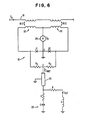
- Figure 7 shows a cascade of two SQUID stages 10, 10' coupled by the filter network 28.
- the symbolic representation of Figure 4 is used to represent the SQUID stages.
- the current input signal l in is applied to the first stage, and the current output from the first stage is taken from terminal 3 thereof and applied to the filter circuit 28, appearing as an input signal to the second SQUID stage.
- the current tout through R L is the output current from the amplifier.
- the voltage output V out from the amplifier is taken from superconductor 32.
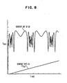
- Figure 8 depicts the output characteristic of a two-SQUID cascade of the type shown in Figure 7. This is a plot of the current tout from the second stage of the amplifier as a function of time, for a current l in which is a linearly increasing ramp. Normally, an operating point for the cascade would be chosen by adding a bias current to l in as was explained with respect to Figure 2. The bias current would be such that the operating point would be on one of the steep sections of the curve for lout shown in Figure 8.
- the dynamic range of the output is limited to the voltage modulation depth of the output stage of the two-stage cascade.
- the dynamic range of the input is limited to approximately the output dynamic range divided by the slope (gain) at the operating point.
- Figure 8 is a computer simulation of the operation of the two-SQUID cascade of Figure 7, where the gain of the cascade is approximately 90.
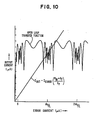
- Figure 10 is a graphical solution of the operating points of the SQUID cascade of Figure 9, where the output current is plotted against the "error current".
- the operating point of this circuit can be chosen without resorting to any ancillary bias.
- the error current represents the current flowing in the input coil to the first SQUID stage 10.
- the open loop characteristic (as in Figure 8) is plotted against the error current.
- the output current required to produce a given error current is plotted against error current, assuming zero input signal to SQUID 10, and taking into account the current split between R Io and R f in the circuit of Figure 9.
- Possible operating points exist wherever the straight line (l out ) and the open loop characteristic intersect. By changing the ratio of R f to R in , the operating point (defined as the intersection of tout and the open loop transfer function) can be moved.
- Figures 11 and 12 are simulations of the amplifier in operation with the negative feedback loop closed.
- Figure 11 shows the pulse response of the amplifier, plotting the current output which occurs in response to an input pulse 36 against time.
- Curve 38 shows the initial transients 40 occurring in the amplifier due to the onset of power.
- the pulse response 42 rests on a DC level determined by the bias to the amplifier.
- Figure 12 is the response of the amplifier to a linear ramp 44. Again, transients 46 occur before the linear output 48 is seen in the output current.
- Figures 11 and 12 illustrate a fairly linear response over the dynamic range of the output stage, and a broadband frequency response of nearly 1GHz.
- the gain in these simulations was between 4 and 5, which is close to the ratio of R in to R f .
- a SQUID cascade has been described using a plurality of stages of DC SQUID's, where the stages are coupled in a manner to provide efficient current transfer between stages, in order to provide an amplifier having a bandwidth greater than that previously obtained in SQUID circuits, for the same sensitivity.
- the principles described for coupling SQUID stages can be exemplified by circuits other than those shown herein, the principle of invention being that the current through the shunt resistors of the first SQUID stage can be delivered to the second SQUID stage by a coupling network whose impedance is real up to a high frequency, and whose impedance will match that of a coupling transmission line. This impedance is sufficiently small that essentially all of the current is transferred from the first SQUID stage to the second SQUID stage, but is large enough that the bandwidth of the amplifier is large.
Landscapes
- Physics & Mathematics (AREA)
- Condensed Matter Physics & Semiconductors (AREA)
- General Physics & Mathematics (AREA)
- Superconductor Devices And Manufacturing Methods Thereof (AREA)
- Measuring Magnetic Variables (AREA)
- Electronic Switches (AREA)
Claims (2)
Applications Claiming Priority (2)
| Application Number | Priority Date | Filing Date | Title |
|---|---|---|---|
| US362581 | 1982-03-29 | ||
| US06/362,581 US4496854A (en) | 1982-03-29 | 1982-03-29 | On-chip SQUID cascade |
Publications (2)
| Publication Number | Publication Date |
|---|---|
| EP0090220A1 EP0090220A1 (fr) | 1983-10-05 |
| EP0090220B1 true EP0090220B1 (fr) | 1985-12-27 |
Family
ID=23426662
Family Applications (1)
| Application Number | Title | Priority Date | Filing Date |
|---|---|---|---|
| EP83102355A Expired EP0090220B1 (fr) | 1982-03-29 | 1983-03-10 | Circuit "squid" supraconductif |
Country Status (4)
| Country | Link |
|---|---|
| US (1) | US4496854A (fr) |
| EP (1) | EP0090220B1 (fr) |
| JP (1) | JPS58173877A (fr) |
| DE (1) | DE3361600D1 (fr) |
Families Citing this family (47)
| Publication number | Priority date | Publication date | Assignee | Title |
|---|---|---|---|---|
| JPS60109314A (ja) * | 1983-11-17 | 1985-06-14 | Tsutomu Yamashita | 超伝導増巾回路 |
| JPS60247311A (ja) * | 1984-05-22 | 1985-12-07 | Mitsubishi Electric Corp | 直流超伝導量子干渉素子を用いた増幅装置 |
| EP0205120B1 (fr) * | 1985-06-07 | 1994-09-14 | Hitachi, Ltd. | Circuit détecteur supraconducteur |
| DE3529815A1 (de) * | 1985-08-20 | 1987-02-26 | Siemens Ag | Messvorrichtung mit einem squid-magnetometer |
| DE3738369C1 (de) * | 1987-11-12 | 1988-11-03 | Dornier System Gmbh | Analog/-Digital-Wandler mit interner Rueckkopplung |
| US4983971A (en) * | 1989-06-29 | 1991-01-08 | Westinghouse Electric Corp. | Josephson analog to digital converter for low-level signals |
| US5021658A (en) * | 1989-06-29 | 1991-06-04 | Westinghouse Electric Corp. | Superconducting infrared detector |
| US5053834A (en) * | 1990-08-31 | 1991-10-01 | Quantum Magnetics, Inc. | High symmetry dc SQUID system |
| US5420100A (en) * | 1991-04-05 | 1995-05-30 | Northeastern University | Planar squid magnetometer with inductively coupled microstrip resonator |
| US5126568A (en) * | 1991-07-19 | 1992-06-30 | Grumman Aerospace Corporation | Magnetometer input circuit for infrared detectors |
| US5331162A (en) * | 1991-11-22 | 1994-07-19 | Trw Inc. | Sensitive, low-noise superconducting infrared photodetector |
| US5491334A (en) * | 1994-08-22 | 1996-02-13 | Grumman Aerospace Corporation | Magneto-optical input system for infrared detectors |
| US5798722A (en) * | 1997-02-13 | 1998-08-25 | Northrop Grumman Corporation | UHF digital to analog converter for cryogenic radar system |
| FI112399B (fi) * | 1998-08-28 | 2003-11-28 | Neuromag Oy | Menetelmä ja laite taustahäiriön poistamiseksi monikanavaisista ilmaisinasetelmista |
| US6154044A (en) * | 1998-11-20 | 2000-11-28 | Trw Inc. | Superconductive logic gate and random access memory |
| US7057867B1 (en) * | 2004-05-21 | 2006-06-06 | National Semiconductor Corporation | Electrostatic discharge (ESD) protection clamp circuitry |
| US7533068B2 (en) | 2004-12-23 | 2009-05-12 | D-Wave Systems, Inc. | Analog processor comprising quantum devices |
| US7619437B2 (en) * | 2004-12-30 | 2009-11-17 | D-Wave Systems, Inc. | Coupling methods and architectures for information processing |
| US7898282B2 (en) * | 2005-04-26 | 2011-03-01 | D-Wave Systems Inc. | Systems, devices, and methods for controllably coupling qubits |
| US7468630B2 (en) * | 2006-08-25 | 2008-12-23 | Hypres, Inc. | Superconducting switching amplifier |
| CA2669816C (fr) | 2006-12-05 | 2017-03-07 | D-Wave Systems, Inc. | Systemes, procedes et appareil de programmation locale d'elements de processeur quantique |
| US8195596B2 (en) * | 2007-01-12 | 2012-06-05 | D-Wave Systems Inc. | Systems, devices, and methods for interconnected processor topology |
| CA2672695A1 (fr) * | 2007-01-23 | 2008-07-31 | D-Wave Systems, Inc. | Systemes, dispositifs et procedes permettant de coupler de maniere regulable des bits quantiques |
| US8234103B2 (en) | 2007-04-05 | 2012-07-31 | D-Wave Systems Inc. | Physical realizations of a universal adiabatic quantum computer |
| US7800395B2 (en) * | 2007-05-02 | 2010-09-21 | D-Wave Systems Inc. | Systems, devices, and methods for controllably coupling qubits |
| US7880529B2 (en) * | 2007-09-25 | 2011-02-01 | D-Wave Systems Inc. | Systems, devices, and methods for controllably coupling qubits |
| US8102185B2 (en) * | 2008-01-28 | 2012-01-24 | D-Wave Systems Inc. | Systems, devices, and methods for controllably coupling qubits |
| US7786748B1 (en) * | 2009-05-15 | 2010-08-31 | Northrop Grumman Systems Corporation | Method and apparatus for signal inversion in superconducting logic gates |
| US8571614B1 (en) | 2009-10-12 | 2013-10-29 | Hypres, Inc. | Low-power biasing networks for superconducting integrated circuits |
| WO2014197048A2 (fr) | 2013-03-11 | 2014-12-11 | Massachusetts Institute Of Technology | Dispositif supraconducteur à trois bornes et portes logiques |
| US10002107B2 (en) | 2014-03-12 | 2018-06-19 | D-Wave Systems Inc. | Systems and methods for removing unwanted interactions in quantum devices |
| US9344092B2 (en) * | 2014-08-07 | 2016-05-17 | International Business Machines Corporation | Tunable superconducting notch filter |
| WO2016171875A1 (fr) | 2015-04-03 | 2016-10-27 | Massachusetts Institute Of Technology | Afflux de courant dans des dispositifs supraconducteurs à trois bornes et procédés associés |
| US10222416B1 (en) | 2015-04-14 | 2019-03-05 | Hypres, Inc. | System and method for array diagnostics in superconducting integrated circuit |
| US9461588B1 (en) | 2015-06-09 | 2016-10-04 | Microsoft Technology Licensing, Llc | Doubly balanced josephson junction mixer |
| CN109478255B (zh) | 2016-05-03 | 2023-10-27 | D-波系统公司 | 用于超导电路和可扩展计算中使用的超导装置的系统和方法 |
| CN109964239B (zh) | 2016-06-07 | 2023-08-25 | D-波系统公司 | 用于量子处理器拓扑结构的系统和方法 |
| CN111788588B (zh) | 2017-12-20 | 2024-08-02 | D-波系统公司 | 量子处理器中耦合量子位的系统和方法 |
| WO2019152909A1 (fr) | 2018-02-05 | 2019-08-08 | Massachusetts Institute Of Technology | Processeur programmable à base de nanofils supraconducteurs |
| US11105866B2 (en) | 2018-06-05 | 2021-08-31 | D-Wave Systems Inc. | Dynamical isolation of a cryogenic processor |
| JP7318709B2 (ja) | 2019-07-19 | 2023-08-01 | 日本電気株式会社 | 発振装置、量子計算機、及び制御方法 |
| JP7279792B2 (ja) * | 2019-07-19 | 2023-05-23 | 日本電気株式会社 | 共振器、発振器、及び量子計算機 |
| US11839164B2 (en) | 2019-08-19 | 2023-12-05 | D-Wave Systems Inc. | Systems and methods for addressing devices in a superconducting circuit |
| EP4172883A4 (fr) | 2020-06-30 | 2024-08-14 | D-Wave Systems Inc. | Systèmes et procédés de couplage entre bits quantiques |
| US12501840B2 (en) | 2020-11-24 | 2025-12-16 | D-Wave Systems | Systems, articles, and methods for a tunable capacitor |
| US11533032B2 (en) * | 2021-03-26 | 2022-12-20 | Microsoft Technology Licensing, Llc | Superconducting output amplifiers with interstage filters |
| US12388452B2 (en) | 2021-11-03 | 2025-08-12 | 1372934 B.C. Ltd. | Systems and methods for duty cycle compensation of a digital to analog converter (DAC) |
Family Cites Families (2)
| Publication number | Priority date | Publication date | Assignee | Title |
|---|---|---|---|---|
| US4051393A (en) * | 1976-12-16 | 1977-09-27 | Bell Telephone Laboratories, Incorporated | Current switched josephson junction memory and logic circuits |
| US4280095A (en) * | 1979-03-22 | 1981-07-21 | The United States Of America As Represented By The Secretary Of The Navy | Extremely sensitive super conducting quantum interference device constructed as a double-helix array |
-
1982
- 1982-03-29 US US06/362,581 patent/US4496854A/en not_active Expired - Lifetime
-
1983
- 1983-02-28 JP JP58031066A patent/JPS58173877A/ja active Granted
- 1983-03-10 DE DE8383102355T patent/DE3361600D1/de not_active Expired
- 1983-03-10 EP EP83102355A patent/EP0090220B1/fr not_active Expired
Also Published As
| Publication number | Publication date |
|---|---|
| JPS58173877A (ja) | 1983-10-12 |
| JPS6126239B2 (fr) | 1986-06-19 |
| EP0090220A1 (fr) | 1983-10-05 |
| US4496854A (en) | 1985-01-29 |
| DE3361600D1 (en) | 1986-02-06 |
Similar Documents
| Publication | Publication Date | Title |
|---|---|---|
| EP0090220B1 (fr) | Circuit "squid" supraconductif | |
| US7772871B2 (en) | Method and apparatus for high density superconductor circuit | |
| EP3170259B1 (fr) | Système de déphasage supraconducteur | |
| US4585999A (en) | Radiofrequency amplifier based on a dc superconducting quantum interference device | |
| EP0545948B1 (fr) | Systeme de squid (dispositif d'interference quantique supraconducteur) a courant continu, ayant une tres grande symetrie | |
| CA2225803C (fr) | Dispositif et procede relatifs a l'information numerique | |
| Harada et al. | Basic operations of the quantum flux parametron | |
| US6483339B1 (en) | Single flux quantum series biasing technique using superconducting DC transformer | |
| US4621203A (en) | Transformer built of coupled flux shuttles | |
| Adelerhof et al. | (Double) relaxation oscillation SQUIDs with high flux‐to‐voltage transfer: Simulations and experiments | |
| AU2019240774B2 (en) | Superconducting quantum interference apparatus | |
| JP4066012B2 (ja) | 超電導ドライバ回路及び超電導機器 | |
| US4509018A (en) | Asymmetric superconducting quantum interference device in a linear amplifier circuit | |
| US3725819A (en) | Supercurrent devices with enhanced self-field effects | |
| Hioe | Quantum flux parametron: a single quantum flux superconducting logic device | |
| EP0074666B1 (fr) | Circuit utilisant l'effet Josephson | |
| Newhouse et al. | An ultrasensitive linear cryotron amplifier | |
| Martens et al. | S-parameter measurements and microwave applications of superconducting flux flow transistors | |
| Foglietti et al. | Performance of a flux locked series SQUID array | |
| US4342924A (en) | Nonhysteretic Josephson junction circuits with feedback | |
| McDonald | Superconducting electronics | |
| Radparvar et al. | An integrated digital SQUID magnetometer with high sensitivity input | |
| Adelerhof et al. | Relaxation oscillation SQUIDs with high delta V/delta Phi | |
| Adelerhof et al. | High sensitivity magnetic flux sensors with direct voltage readout: double relaxation oscillation SQUIDs | |
| Satchell et al. | Arrays of high temperature superconductor Josephson junctions |
Legal Events
| Date | Code | Title | Description |
|---|---|---|---|
| PUAI | Public reference made under article 153(3) epc to a published international application that has entered the european phase |
Free format text: ORIGINAL CODE: 0009012 |
|
| AK | Designated contracting states |
Designated state(s): DE FR GB |
|
| 17P | Request for examination filed |
Effective date: 19840126 |
|
| GRAA | (expected) grant |
Free format text: ORIGINAL CODE: 0009210 |
|
| AK | Designated contracting states |
Designated state(s): DE FR GB |
|
| REF | Corresponds to: |
Ref document number: 3361600 Country of ref document: DE Date of ref document: 19860206 |
|
| ET | Fr: translation filed | ||
| PLBE | No opposition filed within time limit |
Free format text: ORIGINAL CODE: 0009261 |
|
| STAA | Information on the status of an ep patent application or granted ep patent |
Free format text: STATUS: NO OPPOSITION FILED WITHIN TIME LIMIT |
|
| 26N | No opposition filed | ||
| GBPC | Gb: european patent ceased through non-payment of renewal fee | ||
| PG25 | Lapsed in a contracting state [announced via postgrant information from national office to epo] |
Ref country code: GB Effective date: 19881122 |
|
| PGFP | Annual fee paid to national office [announced via postgrant information from national office to epo] |
Ref country code: FR Payment date: 19890223 Year of fee payment: 7 |
|
| PG25 | Lapsed in a contracting state [announced via postgrant information from national office to epo] |
Ref country code: FR Effective date: 19901130 |
|
| REG | Reference to a national code |
Ref country code: FR Ref legal event code: ST |
|
| PGFP | Annual fee paid to national office [announced via postgrant information from national office to epo] |
Ref country code: DE Payment date: 19920321 Year of fee payment: 10 |
|
| PG25 | Lapsed in a contracting state [announced via postgrant information from national office to epo] |
Ref country code: DE Effective date: 19931201 |