EP0090330A2 - Appareil d'opération arithmétique utilisant des cellules solaires - Google Patents
Appareil d'opération arithmétique utilisant des cellules solaires Download PDFInfo
- Publication number
- EP0090330A2 EP0090330A2 EP83102835A EP83102835A EP0090330A2 EP 0090330 A2 EP0090330 A2 EP 0090330A2 EP 83102835 A EP83102835 A EP 83102835A EP 83102835 A EP83102835 A EP 83102835A EP 0090330 A2 EP0090330 A2 EP 0090330A2
- Authority
- EP
- European Patent Office
- Prior art keywords
- voltage
- power source
- source voltage
- lsi
- clock signal
- Prior art date
- Legal status (The legal status is an assumption and is not a legal conclusion. Google has not performed a legal analysis and makes no representation as to the accuracy of the status listed.)
- Granted
Links
Images


Classifications
-
- G—PHYSICS
- G06—COMPUTING OR CALCULATING; COUNTING
- G06F—ELECTRIC DIGITAL DATA PROCESSING
- G06F1/00—Details not covered by groups G06F3/00 - G06F13/00 and G06F21/00
- G06F1/24—Resetting means
-
- G—PHYSICS
- G06—COMPUTING OR CALCULATING; COUNTING
- G06F—ELECTRIC DIGITAL DATA PROCESSING
- G06F1/00—Details not covered by groups G06F3/00 - G06F13/00 and G06F21/00
- G06F1/26—Power supply means, e.g. regulation thereof
- G06F1/30—Means for acting in the event of power-supply failure or interruption, e.g. power-supply fluctuations
-
- Y—GENERAL TAGGING OF NEW TECHNOLOGICAL DEVELOPMENTS; GENERAL TAGGING OF CROSS-SECTIONAL TECHNOLOGIES SPANNING OVER SEVERAL SECTIONS OF THE IPC; TECHNICAL SUBJECTS COVERED BY FORMER USPC CROSS-REFERENCE ART COLLECTIONS [XRACs] AND DIGESTS
- Y10—TECHNICAL SUBJECTS COVERED BY FORMER USPC
- Y10S—TECHNICAL SUBJECTS COVERED BY FORMER USPC CROSS-REFERENCE ART COLLECTIONS [XRACs] AND DIGESTS
- Y10S323/00—Electricity: power supply or regulation systems
- Y10S323/906—Solar cell systems
Definitions
- the present invention relates to an arithmetic operation apparatus which uses solar cells as a power source and which is used with low power consumption for a compact electronic calculator and an electronic timepiece.
- LSI large scale integrated circuits
- CMOS complementary metal oxide semiconductor
- the development of LSI techniques allows the power source means to be used therefor to be greatly changed.
- Various types of dry cells have been used as the power source means for compact electronic equipment, such as compact electronic calculators and electronic timepieces. More particularly, a compact and lightweight dry cell which has a low current consumption has been adopted along with the low current consumption of the LSI. In this situation, a solar cell has been recently used for the above-mentioned arithmetic operation apparatuses.
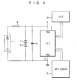
- Fig. 1 is a block diagram showing the general arrangement of a compact electronic calculator using solar cells as the power source.
- solar cells 1 are connected in series with each other.
- the negative terminals of the solar cells 1 are commonly connected to a V DD terminal 4 of an LSI 3 through a resistor 2.
- the V DD terminal 4 supplies a power source voltage V DD (negative voltage).
- the positive terminals of the solar cells 1 are commonly connected to a V SS terminal 5 of the LSI 3.
- the V SS terminal 5 supplies a reference voltage V SS (positive voltage).
- a bypass capacitor 6 is parallel-connected between the V DD terminal 4 and the V SS terminal 5.
- a series circuit of light-emitting diodes (LEDs) 7 and 8 is also parallel-connected between the V DD terminal 4 and the V SS terminal 5.
- the LEDs 7 and 8 serve to prevent a surge voltage from being applied across the LSI 3 when the intensity of light incident on the solar cells 1 is very high.
- the resistor 2 and the capacitor 6 are arranged to prevent variations in the voltage applied across the LSI 3 even if the intensity of light incident on the solar cells 1 is abruptly changed.
- the LSI 3 includes electronic circuits such as an arithmetic and logic unit, an oscillator and a display driver so as to execute a series of operations (i.e., from the execution of various types of operation to the generation of a display signal for displaying the operation results).
- a keyboard 9 and a liquid crystal display (LCD) 10 are connected to the LSI 3.
- Fig. 2 is a graph showing general voltage-current characteristic curves and the load characteristics of the LSI 3, using the illuminance (Lux) as a parameter.
- the power capacity of the solar cells increases when the illuminance increases.
- the power capacity of the solar cells decreases when the illuminance decreases. Therefore, when a solar cell is used as a power source, a constant voltage cannot be obtained, unlike a case in which any cell other than the solar cell, such as a silver-oxide cell, is used.
- An output voltage of the solar cell greatly changes in accordance with changes in the ambient illuminance and the orientation of the solar cell with respect to the light source.
- the compact electronic calculator has two statuses: a control signal reception ready status (i.e., key signal waiting status wherein the LSI 3 awaits a key signal from the keyboard 9); and an operating status wherein any desired operation may be executed after the key signal is received. Although some compact electronic calculators do not have these two statuses, a compact electronic calculator having the two functions is illustrated for the sake of simplicity. In general, the current consumption of the LSI 3 in the operating status is greater than that in the key signal waiting status. This is because the number of active circuits in the operating status is greater than that in the key signal waiting status.
- a line Ll in the graph shown in Fig. 2 indicates the load characteristics of the LSI 3 in the key signal waiting status
- a line L2 indicates the load characteristics in the operation status.
- illuminance is set corresponding to 150 Lux
- a voltage of about -2.22 V corresponding to an intersection between the line Ll and a curve L4 is applied across the LSI 3.
- a voltage of -1.93 V corresponding to an intersection between the line L2 and the curve L4 is applied across the LSI 3.
- the voltage of -2.22 V is changed to -1.93 V.
- the LSI 3 requires a minimum operating voltage V DDmin . If the voltage applied across the LSI 3 becomes lower than the minimum operating voltage V DDmin , the LSI 3 may operate erroneously or become inoperative.
- the voltage V DDmin is about -2 V for an LSI for a compact electronic calculator which has a rated operating voltage of -3 V.
- the LSI operates erroneously or becomes inoperative if illuminance is less than 150 L ux and hence the voltage V DDmin is less than -2 V.
- the apparatus In the conventional arithmetic operation apparatus which has solar cells as the power source, when the intensity of light incident on the solar cells is made lower than a predetermined level, the apparatus operates erroneously or becomes inoperative.
- an object of the present invention to provide an arithmetic operation apparatus using solar cells as a power source, and which may be stably operated across a wider intensity range of light incident on the solar cells.
- an arithmetic operation apparatus using solar cells as a power source comprising: an arithmetic and logic unit for executing various types of operations; a clock signal generator for generating a clock signal to be used as a sync signal in said arithmetic and logic unit; first and second voltage comparators for respectively comparing an absolute value of a first voltage with that of a power source voltage and an absolute value of a second voltage with that of the power source voltage, and for respectively producing logic signals in accordance with the comparison results, the absolute value of the first voltage being smaller than that of the second voltage; and a control circuit for interrupting generation of the clock signal from said clock signal generator when said first voltage comparator determines a coincidence between the absolute values of the first voltage and the power source voltage, and for restarting said clock signal generator when said second voltage comparator determines a coincidence between the absolute values of the second voltage and the power source voltage after a clock signal interruption.
- Fig. 3 shows the internal arrangement of an LSI 3 corresponding to the LSI 3 shown in Fig. 1.
- First and second voltage comparators 21 and 22 respectively compare set voltages Vl and V2 with a power source voltage V DD supplied to the V DD terminal 4 of the LSI 3. The first and second voltage comparators 21 and 22 then produce coincidence signals when the voltage Vl coincides with the power source voltage VDD, and the voltage V2 coincides with the power source voltage V DD' respectively.
- the first voltage comparator 21 produces a high-level signal.
- the first voltage comparator 21 produces a low-level signal.
- the second voltage comparator 22 When the absolute value of the power source voltage V DD is smaller than that of the voltage V2, the second voltage comparator 22 also produces a low-level signal. However, when the absolute value of the power source voltage V DD coincides with that of the voltage V2, the second voltage comparator 22 produces a high-level signal.
- the logic signal from the first voltage comparator 21 is supplied to one input terminal of a 2-input AND gate 24 through an inverter 23.
- the logic signal from the second voltage comparator 22 is supplied to one input terminal of a 2-input AND gate 25.
- a clock signal $ 2 to be described later is supplied to the other input terminal of each of the AND gates 24 and 25.
- An output signal from the AND gate 24 is supplied to one input terminal of a 2-input NOR gate 26, and an output signal from the AND gate 25 is supplied to one input terminal of a 2-input NOR gate 27.
- the other input terminal of the NOR gate 26 is connected to the output terminal of the NOR gate 27, and the other input terminal of the NOR gate 27 is connected to the output terminal of the NOR gate 26.
- the NOR gates 26 and 27 constitute a flip-flop 28.
- An output signal from the NOR gate 27 of the flip-flop 28 is supplied to an oscillator 29.
- a closed loop of an inverter 30, a 2-input NOR gate 31, an inverter 32 and a resistor 33 are formed in the oscillator 29.
- the oscillator 29 further includes: a capacitor 34 connected between the input terminal of the inverter 30 and the output terminal of the NOR gate 31; an inverter 35 for obtaining one oscillation signal CP by inverting the output signal from the NOR gate 31; two inverters 36 and 37 which are series-connected to sequentially invert the output signal from the NOR gate 31 to obtain the other oscillation signal CP.
- the oscillation signal CP corresponds to a signal obtained by inverting the oscillation signal CP.
- the output signal from the flip-flop 28 is supplied to one input terminal of the 2-input NOR gate 31.
- the oscillator 29 comprises a CR oscillator which has the NOR gate 31 as an inhibition gate. When the output signal from the flip-flop 28 is set at a low level, the oscillator 29 is operated to produce the oscillation signals CP and CP of a predetermined frequency.
- the oscillator 29 is kept inoperative by means of the NOR gate 31.
- the oscillation signals CP and CP from the oscillator 29 are supplied to a clock signal generator 38.
- the clock signal generator 38 includes a flip-flop 39 comprising a delay shift register in which a data input terminal D and an output terminal Q are coupled to each other and which is synchronized with the oscillation signals CP and CP.
- the clock signal generator 38 further includes two 2-input AND gates 40 and 41.
- the oscillation signal CP and the Q output signal from the flip-flop 39 are supplied to the AND gate 40 which then produces a signal ⁇ 1 which is one of two clock signals of different phases.
- the AND gate 41 receives the oscillation signal CP and the Q output signal from the flip-flop 39 and produces a signal ⁇ 2 which is the other of the two clock signals of different phases.
- the clock signals $ 1 and $ 2 of different phases produced by the clock signal generator 38 are supplied as sync signals to an arithmetic circuit 42.
- the clock signal ⁇ 2 is also supplied to the other input terminal of each of the 2-input AND gates 24
- the arithmetic circuit 42 executes various types of operations in synchronism with the clock signals of different phases when a key signal is supplied from the keyboard 9.
- the operation results are supplied to an LCD driver 43.
- the LCD driver 43 converts the operation results from the arithmetic circuit 42 to display signals so as to suitably display the operation results at the LCD 10.
- the output signal from the flip-flop 28 is supplied to the LCD driver 43.
- the conversion operation of the LCD driver 43 is controlled by the output signal from the flip-flop 28.
- the minimum operating voltage of the arithmetic circuit 42 is set at -2 V, and the solar cells 1 have the characteristics shown in Fig. 2, the voltage Vl of the first voltage comparator 21 is set at -2.1 V, whereas the voltage V2 of the second voltage comparator 22 is set at -2.5 V.
- the power source voltage V DD is set at a high level and the reference voltage V SS is set at a low level (i.e., the negative logic is adopted).
- the load characteristics of the LSI 3 are indicated by the line Ll.
- the power source voltage V DD applied to the V DD terminal 4 of the LSI 3 is kept at -2.22 V which is obtained at the intersection between the line Ll and the voltage-current characteristic curve L4 of the solar cells 1.
- the absolute value of the power source voltage V DD of -2.22 V is greater than that of the voltage Vl of -2.1 V and is smaller than that of the voltage V2 of -2.5 V.
- the first voltage comparator 21 then produces a high-level signal, whereas the second voltage comparator 22 produces a low-level signal.
- the NOR gate 31 of the oscillator 29 is not then disabled, and serves as an inverter.
- the oscillator 29 is then operated to sequentially produce the oscillation signals CP and CP.
- the clock signal generator sequentially produce the clock signals ⁇ 1 and ⁇ 2 .
- the arithmetic circuit 42 When a key signal is supplied from the keyboard 9 to the LSI 3, the arithmetic circuit 42 is initially set in the operating status. The load characteristics of the LSI 3 which are indicated by the line Ll are then changed to those which are indicated by the line L2. If the capacitance of the capacitor 6 shown in Fig. 1 is set at 5 ⁇ F, and an impedance between the terminals 4 and 5 of the LSI 3 is set at 200 K2, the time constant in the transition (from Ll to L2) of load characteristics of the LSI 3 is 1 second. The power source voltage V DD gradually decreases from -2.22 V obtained at the intersection between the line Ll and the curve L4 to -1.93 V obtained at the intersection between the line L2 and the curve L4.
- the decrease in the power source voltage V DD is sufficiently slower than the arithmetic operation speed of the arithmetic circuit 42.
- the first voltage comparator 21 detects a coincidence between the power source voltage V DD and the voltage Vl of -2.1 V.
- the first voltage comparator 21 then produces a low-level signal, so that the output signal from the inverter 23 goes high.
- the output signal from the flip-flop 28 goes high in response to the output signal from the AND gate 24 in synchronism with the clock signal $ 2 supplied thereto.
- the output signal from the NOR gate 31 is kept low irrespective of the output signal from the inverter 30, thereby interrupting the operation of the oscillator 29.
- the oscillation signal CP is kept high, whereas the oscillation signal CP is kept low. Therefore, the clock signal generator 38 stops generating the clock signals ⁇ 1 and ⁇ 2 .
- the clock signal ⁇ 1 is kept low, whereas the clock signal ⁇ 2 is kept high.
- the clock signals ⁇ 1 and ⁇ 2 are not supplied to the arithmetic circuit 42, and the arithmetic operation of the arithmetic circuit 42 is interrupted, so that internal data therein is held.
- the LCD driver 43 is stopped. It is noted that the arithmetic circuit 42 and the LCD driver 43 are simultaneously stopped, thereby greatly decreasing current consumption.
- the load characteristics of the LSI 3 are changed as indicated by a line LO in Fig. 2. Assume that the resistance of the resistor 2 is set at 1 KQ. Since the capacitance of the capacitor 6 is less than 5 uF, the transition speed from the load characteristics of the LSI 3 as indicated by the line L2 to those indicated by the line LO corresponds to a time constant of 5 msec. The power source voltage V DD applied across the LSI 3 abruptly increases.
- the second voltage comparator 22 detects a coincidence between the power source voltage V DD and the voltage V2 (-2.5 V). The coincidence signal of a high level is then produced by the second voltage comparator 22. Meanwhile, the clock signal $ 2 is kept high after the oscillator 29 is stopped. Therefore, the high-level signal from the second voltage comparator 22 is supplied to the AND gate 25, and the output signal from the AND gate 25 goes high. When the high-level output signal from the AND gate 25 is supplied to the flip-flop 28, the output signal from the flip-flop 28 goes low. When the output signal from the flip-flop 28 goes low, the NOR gate 31 of the oscillator 29 is enabled, thereby restarting the oscillator 29.
- the oscillator 29 sequentially produces the oscillation signals CP and CP.
- the clock signals ⁇ 1 and ⁇ 2 are sequentially produced by the clock signal generator 38.
- the arithmetic circuit 42 is restarted and executes arithmetic operations in synchronism with the clock signals ⁇ 1 and ⁇ 2 .
- the power source voltage V DD is sufficiently greater than the minimum operating voltage of -2 V so the arithmetic circuit 42 will not operate erroneously or become inoperative.
- the LCD driver 43 is enabled so as to receive the operation results from the arithmetic circuit 42 and to convert them to display signals.
- the arithmetic circuit 42 and the LCD driver 43 are simultaneously started.
- the load characteristics of the LSI 3 which are indicated by the line LO are changed to those indicated by the line L2 through those indicated by the line Ll. Since the capacitance of the capacitor 6 is set at 5 ⁇ F and the impedance between the terminals 4 and 5 of the LSI 3 is set at 200 kQ, the time constant of the transition speed is as long as 1 second. At least four or five operations are executed by the arithmetic circuit 42 during this 1-second period. More particularly, the normal operation is completed before the power source voltage reaches the voltage Vl. The LSI 3 is then set in the key signal waiting status.
- the load characteristics of the LSI 3 which are indicated by the line Ll are retained and may not be changed to the level as indicated by the line L2. Even if the power source voltage V DD should reach the voltage Vl before the arithmetic operation is completed, the output signal from the voltage comparator 21 goes low. Therefore, the above-mentioned operation is repeated, and the arithmetic operation is properly performed to its conclusion.
- the oscillator 29, the clock signal generator 38 and the arithmetic circuit 42 are temporarily stopped. While the arithmetic circuit 42 is stopped, the power source voltage V DD is recovered. Then, the clock signals ⁇ 1 and ⁇ 2 are generated by the clock signal generator 38 to restart the arithmetic circuit 42. Therefore, the apparatus can be stably operated across a wider intensity range of light incident on the solar cells 1.
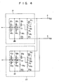
- Fig. 4 shows the detailed arrangement of the first and second voltage comparators 21 and 22 shown in Fig. 3.
- the first and second voltage comparators 21 and 22 have the same arrangement.
- the voltages Vl and V2 are respectively set in the first and second voltage comparators 21 and 22 in accordance with proper adjustments of the internal circuit constants.
- the first voltage comparator 21 comprises: a series circuit 54 1 which has an n-channel MOSFET 51 1 and resistors 52 1 and 53 1 and which is connected between the V DD terminal 4 for supplying the power source voltage V DD and the V SS terminal 5 for supplying the reference voltage V SS ; a series circuit 57 1 which has an n-channel MOSFET 55 1 and a resistor 56 1 and which is connected between the V DD terminal 4 and the V SS terminal 5; a CMOS inverter 60 1 which has an n-channel MOSFET 58 1 and a p-channel MOSFET 59 1 and which is connected between the V DD terminal 4 and the V SS terminal 5; and a CMOS inverter 63 1 which has an n-channel MOSFET 61 1 and a p-channel MOSFET 62 1 and which is connected between the V DD terminal 4 and the V SS terminal 5.
- the MOSFET 51 1 which constitutes a part of the series circuit 54 1 has a gate and drain which are short-circuited. Therefore, the MOSFET 51 1 serves as a constant voltage element.
- a voltage at a node Al between the gate and the drain of the MOSFET 51 1 is set at a voltage (V DD - V TH ) obtained by subtracting the threshold voltage V TH of the MOSFET 51 1 from the power source voltage V DD at the V DD terminal 4.
- the voltage at the node Al is divided by the resistors 52 1 and 53 1 , so that a divided voltage is supplied to the gate of the MOSFET 55 1 .
- resistances of the resistors 52 1 and 53 1 are given as Rll and R12, respectively.
- a voltage V B1 at a node Bl between the resistors 52 1 and 53 1 is then given as follows:
- the MOSFET 55 1 of the series circuit 57 1 which receives the voltage V B1 at its gate is turned on/off in accordance with the voltage V Bl .
- the MOSFET 55 1 is turned on in accordance with the voltage V B1
- the ON resistance of the MOSFET 55 1 and the resistance of the resistor 56 1 are given as R ONl and R13, respectively.
- is equal to
- V DD the gate-source voltage
- decreases, and the ON resistance R ONl of the MOSFET 55 1 increases.
- a change in the ON resistance R ONl of the MOSFET 55 1 can be controlled by properly selecting the resistance R13. Therefore, when the power source voltage V DD comes close to 0 V and reaches a predetermined voltage, the voltage V Cl at the node Cl can be controlled to abruptly come close to 0 V.
- the voltage V Cl is sequentially inverted and amplified by the CMOS inverters 60 1 and 63 1 .
- the output signal from the CMOS inverter 60 1 goes high level (V DD level).
- the output signal from the CMOS inverter 63 1 then goes low (V SS level).
- the first voltage comparator 21 compares the internal set voltage with the power source voltage V DD and produces a logic signal in accordance with a comparison result.
- the resistance R13 of the resistor 56 1 and any other circuit constant such as the threshold voltage of the MOSFET 55 1 can be properly determined.
- the second voltage comparator circuit 22 comprises: a series circuit 54 2 which has an n-channel MOSFET 51 2 and resistors 52 2 and 53 2 ; a series circuit 57 2 which has an n-channel MOSFET 55 and a resistor 56 2 ; a CMOS inverter 60 2 which comprises an n-channel MOSFET 58 2 and a p-channel MOSFET 59 2 ; and a CMOS inverter 63 2 which comprises an n-channel MOSFET 61 2 and a p-channel MOSFET 62 2 .
- the resistance of the resistor 56 2 , the threshold voltage of the MOSFET 55 2 and the like may be properly determined in the same manner as for the first voltage comparator 21.
- the present invention is applied to a compact electronic calculator.
- the present invention can also be applied to any other arithmetic operation apparatus using solar cells as a power source.
Landscapes
- Engineering & Computer Science (AREA)
- Theoretical Computer Science (AREA)
- Physics & Mathematics (AREA)
- General Engineering & Computer Science (AREA)
- General Physics & Mathematics (AREA)
- Calculators And Similar Devices (AREA)
- Power Sources (AREA)
- Direct Current Feeding And Distribution (AREA)
Applications Claiming Priority (2)
| Application Number | Priority Date | Filing Date | Title |
|---|---|---|---|
| JP52024/82 | 1982-03-30 | ||
| JP57052024A JPS58168122A (ja) | 1982-03-30 | 1982-03-30 | 演算処理装置 |
Publications (3)
| Publication Number | Publication Date |
|---|---|
| EP0090330A2 true EP0090330A2 (fr) | 1983-10-05 |
| EP0090330A3 EP0090330A3 (en) | 1985-03-13 |
| EP0090330B1 EP0090330B1 (fr) | 1988-05-18 |
Family
ID=12903239
Family Applications (1)
| Application Number | Title | Priority Date | Filing Date |
|---|---|---|---|
| EP83102835A Expired EP0090330B1 (fr) | 1982-03-30 | 1983-03-22 | Appareil d'opération arithmétique utilisant des cellules solaires |
Country Status (4)
| Country | Link |
|---|---|
| US (1) | US4571690A (fr) |
| EP (1) | EP0090330B1 (fr) |
| JP (1) | JPS58168122A (fr) |
| DE (1) | DE3376695D1 (fr) |
Cited By (2)
| Publication number | Priority date | Publication date | Assignee | Title |
|---|---|---|---|---|
| EP0208986A1 (fr) * | 1985-07-06 | 1987-01-21 | Junghans Uhren Gmbh | Appareil miniature électrique alimenté par cellules solaires, en particulier montre solaire |
| EP0591561A1 (fr) * | 1992-09-30 | 1994-04-13 | Siemens Aktiengesellschaft | Circuit intégré pour générer un signal de remise à l'état initial |
Families Citing this family (11)
| Publication number | Priority date | Publication date | Assignee | Title |
|---|---|---|---|---|
| JPS62225180A (ja) * | 1986-03-26 | 1987-10-03 | Murata Mfg Co Ltd | 放電管用高圧電源 |
| JPS6375877U (fr) * | 1986-11-07 | 1988-05-20 | ||
| US5339446A (en) * | 1986-12-26 | 1994-08-16 | Kabushiki Kaisha Toshiba | Power supply and method for use in a computer system to confirm a save operation of the computer system and to stop a supply of power to the computer system after confirmation |
| JPH0255590A (ja) * | 1988-08-16 | 1990-02-23 | Mitsubishi Electric Corp | モータ制御装置 |
| US5287286A (en) * | 1989-07-31 | 1994-02-15 | Kabushiki Kaisha Toshiba | Low-battery state detecting system and method for detecting the residual capacity of a battery from the variation in battery voltage |
| JP3291011B2 (ja) * | 1990-11-30 | 2002-06-10 | ナルデック株式会社 | 太陽電池を有する車両の電子デバイスのための保護装置 |
| JPH11202968A (ja) * | 1998-01-20 | 1999-07-30 | Mitsubishi Electric Corp | マイクロコンピュータ |
| US6348908B1 (en) * | 1998-09-15 | 2002-02-19 | Xerox Corporation | Ambient energy powered display |
| JP2004191333A (ja) | 2002-12-13 | 2004-07-08 | Matsushita Electric Ind Co Ltd | 2値電源電圧検出回路 |
| JP2008141013A (ja) * | 2006-12-01 | 2008-06-19 | Matsushita Electric Ind Co Ltd | 半導体装置 |
| US8063866B2 (en) * | 2007-11-15 | 2011-11-22 | Toshiba Matsushita Display Technology Co., Ltd. | Display device capable of measuring an illuminance and widening a dynamic range of the measured illuminance |
Family Cites Families (9)
| Publication number | Priority date | Publication date | Assignee | Title |
|---|---|---|---|---|
| JPS5013524B1 (fr) * | 1969-04-30 | 1975-05-20 | ||
| JPS584393B2 (ja) * | 1973-07-04 | 1983-01-26 | ミタニシヨウジ カブシキガイシヤ | 硬貨選別装置の為の選別発振回路 |
| US4264962A (en) * | 1978-02-07 | 1981-04-28 | Beam Engineering Kabushiki Kaisha | Small-sized electronic calculator |
| US4234920A (en) * | 1978-11-24 | 1980-11-18 | Engineered Systems, Inc. | Power failure detection and restart system |
| US4333136A (en) * | 1979-11-26 | 1982-06-01 | Baker Richard H | Solar powered automatic turn-on control (SPA-TOC) unit and method |
| US4375662A (en) * | 1979-11-26 | 1983-03-01 | Exxon Research And Engineering Co. | Method of and apparatus for enabling output power of solar panel to be maximized |
| JPS56147254A (en) * | 1980-04-18 | 1981-11-16 | Canon Inc | Electronic apparatus |
| JPS57208733A (en) * | 1981-06-18 | 1982-12-21 | Fujitsu Ltd | Preventing circuit for malfunction |
| US4428020A (en) * | 1981-10-14 | 1984-01-24 | Scm Corporation | Power supply sensing circuitry |
-
1982
- 1982-03-30 JP JP57052024A patent/JPS58168122A/ja active Pending
-
1983
- 1983-03-22 DE DE8383102835T patent/DE3376695D1/de not_active Expired
- 1983-03-22 EP EP83102835A patent/EP0090330B1/fr not_active Expired
- 1983-03-29 US US06/480,003 patent/US4571690A/en not_active Expired - Lifetime
Cited By (3)
| Publication number | Priority date | Publication date | Assignee | Title |
|---|---|---|---|---|
| EP0208986A1 (fr) * | 1985-07-06 | 1987-01-21 | Junghans Uhren Gmbh | Appareil miniature électrique alimenté par cellules solaires, en particulier montre solaire |
| EP0591561A1 (fr) * | 1992-09-30 | 1994-04-13 | Siemens Aktiengesellschaft | Circuit intégré pour générer un signal de remise à l'état initial |
| US5442312A (en) * | 1992-09-30 | 1995-08-15 | Siemens Ag | Integrated circuit for generating a reset signal |
Also Published As
| Publication number | Publication date |
|---|---|
| JPS58168122A (ja) | 1983-10-04 |
| EP0090330B1 (fr) | 1988-05-18 |
| DE3376695D1 (en) | 1988-06-23 |
| EP0090330A3 (en) | 1985-03-13 |
| US4571690A (en) | 1986-02-18 |
Similar Documents
| Publication | Publication Date | Title |
|---|---|---|
| US3824447A (en) | Booster circuit | |
| US4571690A (en) | Arithmetic operation apparatus using solar cells | |
| KR100299884B1 (ko) | 낮은항복전압을갖는출력버퍼회로 | |
| US5323066A (en) | Method and apparatus for performing power on reset initialization in a data processing system | |
| US5990753A (en) | Precision oscillator circuit having a controllable duty cycle and related methods | |
| US4653931A (en) | Self-charging electronic timepiece | |
| US4285043A (en) | Power transmission controller for electronic calculators | |
| US11245360B2 (en) | Oscillator circuit, chip and electronic device | |
| US4115706A (en) | Integrated circuit having one-input terminal with selectively varying input levels | |
| GB2142489A (en) | Low power consumption electronic circuit | |
| US6763471B1 (en) | Single chip microcomputer with reduced channel leakage current during a stable low speed operation state | |
| US6388479B1 (en) | Oscillator based power-on-reset circuit | |
| EP0872784B1 (fr) | Circuit oscillateur, circuit électronique utilisant celui-ci, et dispositif sémi-conducteur, appareil électronique, et pièce d'horlogerie utilisant celui-ci | |
| JPH10190416A (ja) | フリップフロップ回路 | |
| US4141064A (en) | Booster circuit | |
| US4825407A (en) | Method and circuit for controlling single chip microcomputer | |
| US5398001A (en) | Self-timing four-phase clock generator | |
| US4365203A (en) | Multi-frequency clock generator with error-free frequency switching | |
| EP0403047B1 (fr) | Circuit diviseur de fréquence | |
| GB2061645A (en) | Power supply system | |
| US3906256A (en) | Drive pulse generator for use in electronic analog display clock apparatus | |
| US4551716A (en) | Display control for electronic calculator | |
| EP0217283A2 (fr) | Circuit pour touche | |
| JPH0795680B2 (ja) | 電圧変換回路 | |
| US4340871A (en) | Low power oscillator having clamping transistors across its timing capacitors |
Legal Events
| Date | Code | Title | Description |
|---|---|---|---|
| PUAI | Public reference made under article 153(3) epc to a published international application that has entered the european phase |
Free format text: ORIGINAL CODE: 0009012 |
|
| 17P | Request for examination filed |
Effective date: 19830419 |
|
| AK | Designated contracting states |
Designated state(s): DE FR GB |
|
| RAP1 | Party data changed (applicant data changed or rights of an application transferred) |
Owner name: KABUSHIKI KAISHA TOSHIBA |
|
| PUAL | Search report despatched |
Free format text: ORIGINAL CODE: 0009013 |
|
| AK | Designated contracting states |
Designated state(s): DE FR GB |
|
| 17Q | First examination report despatched |
Effective date: 19860523 |
|
| GRAA | (expected) grant |
Free format text: ORIGINAL CODE: 0009210 |
|
| AK | Designated contracting states |
Kind code of ref document: B1 Designated state(s): DE FR GB |
|
| REF | Corresponds to: |
Ref document number: 3376695 Country of ref document: DE Date of ref document: 19880623 |
|
| ET | Fr: translation filed | ||
| PLBE | No opposition filed within time limit |
Free format text: ORIGINAL CODE: 0009261 |
|
| STAA | Information on the status of an ep patent application or granted ep patent |
Free format text: STATUS: NO OPPOSITION FILED WITHIN TIME LIMIT |
|
| 26N | No opposition filed | ||
| PGFP | Annual fee paid to national office [announced via postgrant information from national office to epo] |
Ref country code: GB Payment date: 19970313 Year of fee payment: 15 |
|
| PGFP | Annual fee paid to national office [announced via postgrant information from national office to epo] |
Ref country code: DE Payment date: 19970401 Year of fee payment: 15 |
|
| PGFP | Annual fee paid to national office [announced via postgrant information from national office to epo] |
Ref country code: FR Payment date: 19980310 Year of fee payment: 16 |
|
| PG25 | Lapsed in a contracting state [announced via postgrant information from national office to epo] |
Ref country code: GB Free format text: LAPSE BECAUSE OF NON-PAYMENT OF DUE FEES Effective date: 19980322 |
|
| GBPC | Gb: european patent ceased through non-payment of renewal fee |
Effective date: 19980322 |
|
| PG25 | Lapsed in a contracting state [announced via postgrant information from national office to epo] |
Ref country code: DE Free format text: LAPSE BECAUSE OF NON-PAYMENT OF DUE FEES Effective date: 19981201 |
|
| PG25 | Lapsed in a contracting state [announced via postgrant information from national office to epo] |
Ref country code: FR Free format text: LAPSE BECAUSE OF NON-PAYMENT OF DUE FEES Effective date: 19991130 |
|
| REG | Reference to a national code |
Ref country code: FR Ref legal event code: ST |