EP0090421A2 - Logische Schaltung - Google Patents
Logische Schaltung Download PDFInfo
- Publication number
- EP0090421A2 EP0090421A2 EP83103171A EP83103171A EP0090421A2 EP 0090421 A2 EP0090421 A2 EP 0090421A2 EP 83103171 A EP83103171 A EP 83103171A EP 83103171 A EP83103171 A EP 83103171A EP 0090421 A2 EP0090421 A2 EP 0090421A2
- Authority
- EP
- European Patent Office
- Prior art keywords
- logic
- node
- terminal
- field effect
- electrical path
- Prior art date
- Legal status (The legal status is an assumption and is not a legal conclusion. Google has not performed a legal analysis and makes no representation as to the accuracy of the status listed.)
- Ceased
Links
Images

Classifications
-
- H—ELECTRICITY
- H03—ELECTRONIC CIRCUITRY
- H03K—PULSE TECHNIQUE
- H03K19/00—Logic circuits, i.e. having at least two inputs acting on one output; Inverting circuits
- H03K19/02—Logic circuits, i.e. having at least two inputs acting on one output; Inverting circuits using specified components
- H03K19/08—Logic circuits, i.e. having at least two inputs acting on one output; Inverting circuits using specified components using semiconductor devices
- H03K19/094—Logic circuits, i.e. having at least two inputs acting on one output; Inverting circuits using specified components using semiconductor devices using field-effect transistors
- H03K19/0944—Logic circuits, i.e. having at least two inputs acting on one output; Inverting circuits using specified components using semiconductor devices using field-effect transistors using MOSFET or insulated gate field-effect transistors, i.e. IGFET
- H03K19/09441—Logic circuits, i.e. having at least two inputs acting on one output; Inverting circuits using specified components using semiconductor devices using field-effect transistors using MOSFET or insulated gate field-effect transistors, i.e. IGFET of the same canal type
- H03K19/09443—Logic circuits, i.e. having at least two inputs acting on one output; Inverting circuits using specified components using semiconductor devices using field-effect transistors using MOSFET or insulated gate field-effect transistors, i.e. IGFET of the same canal type using a combination of enhancement and depletion transistors
- H03K19/09445—Logic circuits, i.e. having at least two inputs acting on one output; Inverting circuits using specified components using semiconductor devices using field-effect transistors using MOSFET or insulated gate field-effect transistors, i.e. IGFET of the same canal type using a combination of enhancement and depletion transistors with active depletion transistors
Definitions
- the present invention relates to a logic circuit and more particularly to an E/D logic circuit constituted by a depletion mode field-effect transistor (referred to as “D-mode FET” hereinafter) and an enhancement mode field-effect transistor (referred to as “E-mode FET” hereinafter).
- D-mode FET depletion mode field-effect transistor
- E-mode FET enhancement mode field-effect transistor
- an E/D logic circuit e.g., an E/D inverter employing a D-mode FET as a load transistor and an E-mode FET as an input transistor
- an E/D logic circuit has widely been used as a logic circuit integrated in a semiconductor integrated circuit, since such an E/D logic circuit has the following advantages. Namely, the utilization efficiency of the voltage source is high because as a high level of the output a power source level can be obtained as it is without level reduction, and moreover, since the D-mode FET operates as a constant current source, a load capacitance to be driven can be charged at high speed to enhance the switching speed.
- At least one input transistor is made conductive, and via this conducting transistor, a current flows through a D-mode FET as a load.
- the power consumption by this current naturally generates heat, resulting in a rise in temperature of the semiconductor chip, which makes the circuit operation conditions unstable and hinders logic circuits from being arranged with a high density.
- the conventional E/D logic circuit has a large power consumption as well as a limited operating speed. Therefore, it has been difficult to realize a large-scale integration thereof on a semiconductor chip.
- the conventional semiconductor integrated circuit has a power consumption of not greater than about 1 watt in the case where the integration scale is smaller than 2000 gates and can be put into practical use by considering the heat dissipation of the chip.
- the power consumption thereof becomes more than 5 watts, so that the circuit is no more practical.
- the operating speed of the conventional E/D logic circuit is unsatisfactory under the above-mentioned limitation of suppressing the power consumption.
- the total operating speed has been obliged to be unsatisfactory in the circuit formed by cascading logic circuits over a multiplicity of stages.
- an object of the invention to provide an E/D logic circuit which operates with a small power consumption and at a high speed.
- the logic circuit according to the invention has at least two cascaded logic stages.
- the first logic stage has first and second logic sections.
- the first logic section includes an FET for receiving a first input signal and an FET for receiving a second input signal opposite in phase to the first input signal and generates a first output signal
- the second logic section includes an FET for receiving the second input signal and an FET for receiving the first input signal and generates a second output.signal opposite in phase to the first output signal.
- the second logic stage has a third logic section having an FET receiving the first output signal and an FET receiving the second output signal thereby to generate a third output signal, and a fourth logic section having an FET receiving the second output signal and an FET receiving the first output signal thereby to generate a fourth output signal complementary to the third output signal.
- all the first through fourth logic sections are adapted to be driven in a push-pull manner in response to at least a pair of complementary signals and hence hardly consume power.
- each logic section since each logic section has no DC path, the capacitance loaded onto the output of each logic section is connected to only one of a power source and the ground depending on the input state of the logic section, and charged and discharged rapidly. Therefore, each logic section can operate at a high speed.
- the logic circuit according to the invention has logic stages each constituted by a pair of circuits adapted to generate respective output signals complementary to each other in accordance with at least a pair of input signals.
- Such a logic stage has a pair of circuits adapted to operate in a push-pull manner on receipt of at least a pair of input signals and generate output signals complementary to each other.
- the subsequent logic stage which operates on receipt of the outputs of the first-mentioned logic stage is able to operate in a push-pull manner by means of the pair of outputs.
- the logic circuit according to the invention having the above construction will be referred to as "Complementary Push-pull Pair MOS" (CP 3 MOS) hereinafter in connection with the fact that each logic stage is constituted by a pair of push-pull circuits complementary to each other.
- CP 3 MOS Complementary Push-pull Pair MOS
- the CP 3 M OS logic circuit has the following features.
- Fig. 1 showing an inverter circuit as one stage according to the conventional circuit system called the E/D arrangement employing E- and D-mode FETs as constituent elements.
- the drain electrode of a D-mode FET P 1 is connected to a power source V DD , and both the gate and source electrodes thereof are connected to the drain electrode of an E-mode FET Q 1 .
- the source electrode of the FET Q 1 is grounded, and input terminal A and an output terminal Y are led out from the gate and drain electrodes of the FET Q 1 .
- the conventional circuit generally employs the D-mode FET as a constant-current source type load element. Consequently, when the E mode FET Q 1 is in the conducting state, a constant current flows from the power source V DD via the D-mode FET P to the ground, and power is consumed. The conventional circuit is unable to decrease effectively the power consumed at that time due to the following reason.
- the time required to charge a parasitic capacitance C 1 present between the output terminal Y and the ground so that the state of potential at the output terminal Y is inverted is substantially inversely proportional to the above-mentioned constant current flowing through the D-mode FET P 1 . Consequently, if the above-mentioned power consumed when the E-mode FET Q 1 is in the conducting state is contrived to be smaller, the operating speed of the inverter is inevitably lowered.
- the E-mode FET Q 1 Immediately before the time t 0 , the E-mode FET Q 1 is in the conducting state, therefore, the output potential V Y is 0 V on the assumption that ß D /ß E ⁇ O.
- the gate potential of the E-mode FET Q 1 is 0[v], therefore, the E-mode FET Q 1 is in the nonconducting state on the assumption that V TE > 0[V]. and the parasitic capacitant C 1 present between the output terminal Y and the ground is charged through the D-mode FET P 1 functioning as a constant-current source.
- the output potential Vy rises to be equal to the high potential V DD and thereafter the output potential is maintained constant at the high potential V DD . In this case, the time required for the output potential Vy to become V DD/ 2 after the time to is expressed by tp dr .
- the gate potential of the E-mode FET Q 1 becomes the high potential V DD' therefore, the E-mode FET Q 1 is made conductive, causing the electric charge stored in the capacitor C 1 until the time t 1 to be started to be discharged. Consequently, the output potential V Y lowers from the value V DD' and after the time has sufficiently passed, the output potential Vy becomes O[V] on the assumption that ß D /ß E ⁇ 0 and thereafter the output potential is maintained constant at 0[V].
- an average power consumption W 1 of the conventional inverter circuit is calculated during one period from the time t 0 to the time t 2 .
- the energy P L consumed from the time to to the time t 1 , i.e., during the period T L t 1 -t 0 , is represented as follows: P L CV DD 2 J
- T H denotes the period that V A takes a high level within one cycle period T as shown in Fig. 2. Therefore, the average power consumption W 1 is calculated from the following formula:
- First-stage logic sections C 1A and C 1B generate outputs Y 1 and Y 1 on receipt of pairs of input signal systems (A 1 , A 1 ) and (A 1 , A 1 ), respectively.
- each of the signal systems (A 1 , A 1 ) may be either a single bit signal (a 1 , a 1 ) or a group of signals of a plurality of bits (a 1 , b 1 ... )(a 1 , b 1 ... ) as long as the signals constituting the signal systems are complementary to each other.
- the logic section C 1A has switching circuits S 1 and S 2 series-connected between a power source V DD and the ground, and an output signal Y 1 is drawn out from an intermediate connection point between the circuits S 1 and S 2 .
- the switching circuit S 1 has the signal A 1 fed thereto, while the switching circuit S 2 has the signal A 1 fed thereto so that either one of the two switching circuits S 1 and S 2 is turned ON and the other is turned OFF.
- the switching circuit S 1 is OFF, while the switching circuit S 2 is ON, and the output signal Y 1 has a ground level.
- Each of the switching circuits S 1 and S 2 is constituted by a single FET in the case where each of the signal systems A 1 and A 1 is a single bit signal.
- a plurality of FETs are connected in parallel or series so as to function as each of the switching circuits S 1 and S 2 .
- Each of switching circuits S 3 through S 8 is also constituted by any desired number of FETs in the input signal system fed thereto.
- the logic section C 1B includes the switching circuit S 3 having the signal system A 1 fed thereto and the switching circuit S 4 having the signal system A 1 fed thereto. These switching circuits S 3 and S 4 are connected in series between the power source V DD and the ground, and from an intermediate connection point between the circuits S 3 and S 4 an output signal Y 1 is obtained which is complementary to the output Y 1 of the logic section C 1A . Each of pairs of the switching circuits (S 1 , S 2 ) and (S 3 , S 4 ) is adapted to operate in a push-pull manner in response to the signal systems A and A 1 .
- Second-stage logic sections C 2A and C 2B are constituted by the switching circuits S 5 through S 8 so as to receive the signals Y 1 and Y 1 as inputs and deliver output signals Y 2 and Y 2 complementary to each other, respectively.
- the switching circuits S 5 and S 6 are adapted to operate in a push-pull manner in response to the signals Y 1 and Y 1 fed thereto respectively, while the switching circuits S 7 and S 8 are adapted to operate in a push-pull manner in response to the signals Y 1 and Y 1 fed thereto respectively.
- complementary signals B and B delivered from other sections may be fed to the logic sections C 2A and C2B, as shown in Fig. 3, to constitute the circuits S 5 through S 8 .
- all the logic sections are adapted to operate in a push-pull manner in response to the respective complementary signal systems. Therefore, no DC path is produced at all, and the logic circuit operates with a low power consumption.
- the capacitance loaded onto the output of each logic section is rapidly charged and discharged through the corresponding switching circuit turned ON, it is possible to realize a high-speed operation.
- the gate electrodes of a pair of FETs are connected to a pair of terminals (A, A), respectively.
- the drain and source electrodes of the D-mode FET P 1 are connected to a power source terminal V DD and an output terminal Y, respectively.
- the drain and source electrodes of the E-mode FET Q 1 are connected to the output terminal Y and the ground, respectively, to form a circuit C 1A '
- the gate electrodes of a pair of FETs (P 2' Q 2 ) are connected to the pair of terminals (A, A), respectively.
- the drain and source electrodes of the D-mode FET Q 2 are connected to the power source terminal V DD and the output terminal Y, respectively, while the drain and source electrodes of the E-mode FET P 2 are connected to the output terminal Y and the ground, respectively, to form a circuit C 1B , thereby constituting a pair of circuits (C 1A , C 1B ).
- a parasitic capacitance C 1 (C 2 ) is present between the output terminal Y (Y) and the ground.
- the propagation delay t pa ' of the inverte circuit pair as one stage in accordance with this embodiment will be calculated as follows.
- Fig. 5 shows currents I P1 and I Q2 flowing through the respective D-mode FETs P 1 and Q 2 and potentials Vy and V Y at the respective terminals Y and Y, with the horizontal axis taken as a time axis, in case of applying to the input terminal A(A) shown in Fig.
- the FETs P 1 , Q 1 and Q 2 are in the conducting state, while the FET P 2 is in the nonconducting state, and on the assumption that ß D /ß E ⁇ 0, the output potential Vy is 0 [V] , while the output potential Vy is as high as V DD .
- the gate potentials of the FETs Q 1 and Q 2 are 0 [V] , while the gate potentials of the FETs P 1 and P 2 are as high as V DD .
- the E-mode FET P 2 is in the conducting state, while t-he D-mode FET Q 2 is in a conducting state closer to the nonconducting state than that immediately before the time t 0 ', so that the electric charge stored in the capacitance C 2 until the time t 0 ' is started to be discharged through the E-mode FET P 2 . Consequently, the output potential V Y at the output terminal Y lowers with time, and after the time has sufficiently passed, the output potential Vy becomes 0 V and thereafter, it is maintained constant at a voltage of 0 V.
- the time required for the output potential V Y (V Y ,) to become V DD/ 2 after the time t 0 ' is expressed by t pdr (t pdf ") .
- the gate potentials of the respective FETs Q 1 and Q 2 are V DD' while the gate potentials of the respective FETs P 1 and P 2 are low 0 [V] . Consequently, the FET Q 1 is in the conducting state, while the FET P 1 is in a conducting stage closer to the nonconducting state than that immediately before the time t 1 " so that the electric charge stored in the capacitance C 1 until the time t' 1 is started to be discharged through the FET Q 1 . Accordingly, the output potential Vy lowers from the value V DD toward the value 0 [V] .
- the circuit C 1A delivers a low potential 0 [V] to the output terminal Y.
- the circuit C 1B delivers an output potential V DD .
- the time required for the output potential Vy(Vy) to become V DD/ 2 after the time t 1 is expressed by t pdf (t pdr ").
- the inverter circuit pair (C 1A , C 1B ) deliver potentials (signals) different from each other to the output terminals of the circuits C 1A and C 1B in response to the input signals fed to the input terminal pair, respectively.
- ) 2 , t pdf ' CV DD /ß E (DD -V TE) 2 . Therefore, the delay-power product t pd ' of the embodiment is calculated from the following formula:
- an average power consumption W' of the inverter circuit pair (C 1A , C 1B ) in accordance with the embodiment will be calculated during one period T' from the time t 0 ' to the time t 2 '.
- the average power consumption W' is calculated from the following formula:
- the average power consumption per stage formed by one inverter circuit pair agrees with the above-mentioned W', owing to the symmetricalness between the circuit pair, independently of the number of inverter stages even in the case where an inverter circuit pair arrangement with n stages is imagined which is obtained by cascading n number of circuit pairs (C 1A , C l B ), (C 2A , C 2B ), ...
- the inverter circuit pair in accordance with the embodiment has a significant advantage as follows. Namely, as will be apparent from the formulae for calculating the proparation delay tp d ' and tp d " although the propagation delay of the conventional inverter circuit increases in inverse proportion to the square of the threshold voltage I VTD of the D-mode FET, the propagation delay of the inverter circuit pair in accordance with the embodiment hardly depends on the threshold voltage V TD and will never exceed the critical value:
- the required propagation delay exceeds the critical value, it is possible to reduce the average power consumption of the inverter circuit pair to W' ⁇ 2CV DD 2 /T' by decreasing the threshold voltage V TD of each of the D-mode FETs P 1 and Q 2 .
- the reduction in the average power consumption is found to be remarkable since CV DD 2 /T' V DD B D V TD 2 /4 under the general MOS integrated circuit manufacturing conditions.
- Figs. 6(c) and (d) show examples of pattern layouts for the CP 3 MOS and the conventional E/D MOS inverter, respectively.
- Fig. 7(a) shows the calculated t PD as a function of
- the propagation delay t PD improvement in the CP 3 MOS inverter is ascribed to the smaller t PLH .
- the CP 3 MOS inverter's load capacitance is always less than twice that of the conventional E/D MOS, so the CP 3 MOS inverter's t PD in the range
- Power dissipation in the CP 3 MOS inverter is about twice as large as that for the conventional E/D MOS, as shown in Table 1.
- delay-power product is about one-tenth as large as that for a conventional E/D MOS at low
- Fig. 7(a) indicates that the conventional E/D MOS inverter's V TD must be greater than that of the CP 3 MOS inverter to get small propagation delay. Ehen, it is concluded from that the C P 3 MOS circuit has a wider operating voltage range that the conventional E/D MOS circuit.
- V TE + in the conventional E/D MOS inverter V TE + in the conventional E/D MOS inverter.
- V C >V GE ⁇ 0 V corresponds to the logic signal "0”.
- noise margin is V DD - V C for logic signal "1” and is V C - V OL for "0".
- the noise margin for the conventional E/D MOS circuit design is (V DD - V OL )/2 at best.
- the CP 3 MOS inverter noise margin is quite different from that for the conventional E/D MOS.
- noise margin becomes
- V DD -V OL the noise immunity of CP 3 MOS inverter is at least twice as large as that for the conventional E/D MOS.
- the noise margin for the conventional E/D MOS varies with V TE , V TD , B DI ß E' V DD for the logic signal "1". However, for the signal "0", the noise margin is fixed with no relation to V DD . This causes a narrow operating voltage-range and severe circuit design for the conventional E/D MOS.
- the CP 3 MOS inverter's noise margin for both logic signals "0" and "1" is not only proportional to VDD, but is also almost independent from V TE , V TD , ß E , B D . This enables a wide operating voltage range and easy circuit design for the CP 3 MOS circuit.
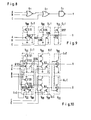
- Fig. 9 shows the conventional E/D logic circuit realizing the circuit of Fig. 8.
- a gate G 1P equivalent to the gate G 1 shown in Fig. 8 is constituted, as is generally known, by a D-mode FET Q 91 as a load and E-mode FETs Q 92 and Q 93 as input transistors.
- a gate G 2P corresponding to the gate G 2 shown in Fig. 8 is constituted by a D-mode FET Q 94 as a load and E-mode FETs Q 95 , Q 96 as input transistors.
- the gate G 3 shown in Fig. 8 is realized as an inverter G 3P constituted by a D-mode FET Q 97 and an E-mode FET Q 98 .
- a DC path is produced when at least one of the three logic gates G l p, G 2 p and G 3P generates a low level signal as its output.
- the logic circuit shown in Fig. 9 when the output Y is low level a DC path is produced in each of the gates G l p and G 3 p, and when the output Y is high level a DC path is produced in the gate G 2P . Therefore, the power consumption is large, and each gate is.adapted to operate in a ratio manner, so that the operating speed is inevitably low.
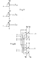
- Fig. 10 shows a practical arrangement of the logic circuit, shown in Fig. 8, realized according to the invention.
- the gate G 1 is constituted by a logic section G 1T adapted to generate outputs A ⁇ B at an output node N 1 on receipt of inputs A, A and B, B, and a logic section G 1C adapted to generate an output A + B at an output node N 2 on receipt of the inputs A, A and B, B similarly.
- the logic section G 1T is a push-pull NOR circuit including D-mode FETs Q 101 and Q 102 which are series-connected between a power source V DD and the output node N 1 and ave the signals Band A applied to their respective gates, and E-mode FETs Q 103 and Q 104 which are parallel-connected between the output node N 1 and the ground and have the signals A and B applied to their respective gates.
- the logic section G 1C is a push-pull OR circuit adapted to generate a logic opposite to that of the section G 1T and delivers the output A + B which is NOT the outputs A ⁇ B of the section G 1T . Consequently, the circuit of the logic section G 1C is constituted by replacing the power source V DD and the ground in the circuit of the section G 1T with each other and moreover employing D-mode FETs Q 107 and Q 108 as the transistors on the power source side.
- the gate G 2 is constituted by a logic section G 2T adapted to receive inputs C and C and the complementary output pair A ⁇ B and the output A +B fed thereto from the logic sections G 1T and G 1C , respectively, and generate the NOR logic thereof, and a logic section G 2C adapted to generate the OR of the above-mentioned inputs.
- the logic section G 2T and the logic section G 2C have the same circuit configurations as the logic section G 1T and the logic section G 1C , respectively.
- a pair of complementary signals generated from the sections G 2T and G 2C are applied to the sections G 3T and G 3C in combination constituting the gate G 3 to generate the outputs Y and Y, respectively.
- the section G 3T or G 3C may be omitted.
- the invention requires to form a pair of complementary signals from the input signals in the case where the input signals applied from the outside are not in the form of a pair of complementary signals.
- the complementary signals can be formed by inverting the input signals through the conventional inverter. More specifically, in order to combine the conventional circuit and the CP 3 MOS circuit by the invention, it is only necessary to employ such inverter circuits as shown in Fig. 11 for forming a pair of signals. Conversely, in case of combining the circuit pair of the invention and the conventional circuit, either one of the pair of signals is employed.
- a semiconductor integrated circuit utilizing a plurality of circuit pairs of the invention in combination offers the following advantages.
- the semiconductor integrated circuit employing the circuit pairs of the invention has signals about twice as many as those generated and coupled in a semiconductor integrated circuit having the same function as the former constituted by combining the conventional circuits.
- Figs. 9 and 10 are compared with each other, that it needs transistors and wirings about twice as many as those in the conventional circuit to realize a logic circuit having the same function as the conventional one by combining a plurality of circuit pairs of the invention.
- the numbers of required transistors and wirings are almost the same as those of the conventional circuit, since although the conventional integrated circuit has necessity to combine basic gates such as inverters, AND circuits, NAND circuits, OR circuits, etc.
- the invention has no necessity to combine basic gates owing to an advantage that any desired logic circuit can be constituted by a gate as one stage due to the fact that it is possible to utilize also the NOT signal of any desired signal simultaneously therewith and that the AND and OR of signals can be obtained by connecting transistors in series and in parallel, respectively.
- the conventional integrated circuit needs 8 transistors, while the invention needs 12 transistor, therefore, the number of transistors required for the invention is not twice but 1.5 times as large as the conventional integrated circuit.
- the invention has the following advantages as described above. Namely, the propagation delay and delay-power product are largely improved, the operating speed is made higher through the reduction in number of logic stages occurring in case of combining a plurality of circuit pairs of the invention, and a ratio-less circuit design is feasible. Therefore, the invention is able to greatly contribute to the realization of a large-scale integrated circuit capable of operating at high speed and with small power consumption.
Landscapes
- Engineering & Computer Science (AREA)
- Power Engineering (AREA)
- Physics & Mathematics (AREA)
- Computer Hardware Design (AREA)
- Computing Systems (AREA)
- General Engineering & Computer Science (AREA)
- Mathematical Physics (AREA)
- Logic Circuits (AREA)
- Electronic Switches (AREA)
Applications Claiming Priority (2)
| Application Number | Priority Date | Filing Date | Title |
|---|---|---|---|
| JP57052031A JPS58170120A (ja) | 1982-03-30 | 1982-03-30 | 半導体集積回路 |
| JP52031/82 | 1982-03-30 |
Publications (2)
| Publication Number | Publication Date |
|---|---|
| EP0090421A2 true EP0090421A2 (de) | 1983-10-05 |
| EP0090421A3 EP0090421A3 (de) | 1984-07-04 |
Family
ID=12903436
Family Applications (1)
| Application Number | Title | Priority Date | Filing Date |
|---|---|---|---|
| EP83103171A Ceased EP0090421A3 (de) | 1982-03-30 | 1983-03-30 | Logische Schaltung |
Country Status (3)
| Country | Link |
|---|---|
| US (1) | US4631424A (de) |
| EP (1) | EP0090421A3 (de) |
| JP (1) | JPS58170120A (de) |
Families Citing this family (7)
| Publication number | Priority date | Publication date | Assignee | Title |
|---|---|---|---|---|
| FR2587516B1 (fr) * | 1985-09-13 | 1987-11-20 | Eurotechnique Sa | Sequenceur d'instructions pour microprocesseur a architecture en reseau |
| US5023480A (en) * | 1990-01-04 | 1991-06-11 | Digital Equipment Corporation | Push-pull cascode logic |
| JP3229164B2 (ja) * | 1994-07-28 | 2001-11-12 | インターナショナル・ビジネス・マシーンズ・コーポレーション | ラッチ回路 |
| US6035110A (en) * | 1996-12-09 | 2000-03-07 | International Business Machines Corporation | Identifying candidate nodes for phase assignment in a logic network |
| US6018621A (en) * | 1996-12-09 | 2000-01-25 | International Business Machines Corporation | Identifying an optimizable logic region in a logic network |
| US5903467A (en) * | 1996-12-10 | 1999-05-11 | International Business Machines Corporation | Selecting phase assignments for candidate nodes in a logic network |
| US10922465B2 (en) * | 2018-09-27 | 2021-02-16 | Arm Limited | Multi-input logic circuitry |
Family Cites Families (4)
| Publication number | Priority date | Publication date | Assignee | Title |
|---|---|---|---|---|
| BE758068A (fr) * | 1969-10-27 | 1971-04-01 | Teletype Corp | Circuits logiques |
| US3953743A (en) * | 1975-02-27 | 1976-04-27 | Rca Corporation | Logic circuit |
| JPS6035756B2 (ja) * | 1977-12-27 | 1985-08-16 | 日本電気株式会社 | 論理回路 |
| US4489246A (en) * | 1980-12-24 | 1984-12-18 | Fujitsu Limited | Field effect transistor logic circuit having high operating speed and low power consumption |
-
1982
- 1982-03-30 JP JP57052031A patent/JPS58170120A/ja active Pending
-
1983
- 1983-03-30 US US06/480,610 patent/US4631424A/en not_active Expired - Lifetime
- 1983-03-30 EP EP83103171A patent/EP0090421A3/de not_active Ceased
Also Published As
| Publication number | Publication date |
|---|---|
| EP0090421A3 (de) | 1984-07-04 |
| JPS58170120A (ja) | 1983-10-06 |
| US4631424A (en) | 1986-12-23 |
Similar Documents
| Publication | Publication Date | Title |
|---|---|---|
| US6154088A (en) | Clocking scheme and charge transfer switch for increasing the efficiency of a charge pump or other circuit | |
| TW476179B (en) | Charge pump circuit applied in low supply voltage | |
| JP2996301B2 (ja) | 負荷及び時間適応電流供給ドライブ回路 | |
| US7586361B2 (en) | Semiconductor device comprising a charge pump operated by clock signals | |
| US20020125935A1 (en) | Semiconductor booster circuit having cascaded MOS transistors | |
| US5270581A (en) | Semiconductor integrated circuit device having step-down circuit associated with component circuits arranged in low-power consumption manner | |
| US6670841B2 (en) | Level shifting circuit | |
| JP3400124B2 (ja) | パストランジスタ型セレクタ回路及び論理回路 | |
| US4628218A (en) | Driving circuit suppressing peak value of charging current from power supply to capacitive load | |
| US5151620A (en) | CMOS input buffer with low power consumption | |
| JPH0897701A (ja) | 半導体回路 | |
| US5300823A (en) | Internal voltage dropping circuit for semiconductor device | |
| US6304120B1 (en) | Buffer circuit operating with a small through current and potential detecting circuit using the same | |
| CN115242106A (zh) | 高频mosfet半桥智能功率模块 | |
| EP0090421A2 (de) | Logische Schaltung | |
| US6838928B2 (en) | Boosting circuit configured with plurality of boosting circuit units in series | |
| EP0095767A2 (de) | Ausgangsschaltung | |
| US5543668A (en) | Charge stacking on-chip high-voltage generator and method | |
| CN115622389A (zh) | 电荷泵电路和存储器 | |
| JP2004153577A (ja) | インバータ回路 | |
| WO2001056084A1 (en) | Low power dissipation mos jam latch | |
| US5457405A (en) | Complementary logic recovered energy circuit | |
| JP3162561B2 (ja) | Cmos論理回路 | |
| Blotti et al. | A comparison of some circuit schemes for semi-reversible adiabatic logic | |
| US6100720A (en) | Low dissipation inverter circuit |
Legal Events
| Date | Code | Title | Description |
|---|---|---|---|
| PUAI | Public reference made under article 153(3) epc to a published international application that has entered the european phase |
Free format text: ORIGINAL CODE: 0009012 |
|
| AK | Designated contracting states |
Designated state(s): DE FR GB IT NL |
|
| RAP1 | Party data changed (applicant data changed or rights of an application transferred) |
Owner name: NEC CORPORATION |
|
| PUAL | Search report despatched |
Free format text: ORIGINAL CODE: 0009013 |
|
| AK | Designated contracting states |
Designated state(s): DE FR GB IT NL |
|
| 17P | Request for examination filed |
Effective date: 19840601 |
|
| STAA | Information on the status of an ep patent application or granted ep patent |
Free format text: STATUS: THE APPLICATION HAS BEEN REFUSED |
|
| 18R | Application refused |
Effective date: 19870322 |
|
| RIN1 | Information on inventor provided before grant (corrected) |
Inventor name: MIYAGI, ISAMU |