EP0090565A2 - Process for selectively cutting an electrical conductive layer by irradiation with an energy beam - Google Patents
Process for selectively cutting an electrical conductive layer by irradiation with an energy beam Download PDFInfo
- Publication number
- EP0090565A2 EP0090565A2 EP83301534A EP83301534A EP0090565A2 EP 0090565 A2 EP0090565 A2 EP 0090565A2 EP 83301534 A EP83301534 A EP 83301534A EP 83301534 A EP83301534 A EP 83301534A EP 0090565 A2 EP0090565 A2 EP 0090565A2
- Authority
- EP
- European Patent Office
- Prior art keywords
- conductive layer
- electrical conductive
- energy beam
- film
- layer
- Prior art date
- Legal status (The legal status is an assumption and is not a legal conclusion. Google has not performed a legal analysis and makes no representation as to the accuracy of the status listed.)
- Granted
Links
Images

Classifications
-
- H—ELECTRICITY
- H10—SEMICONDUCTOR DEVICES; ELECTRIC SOLID-STATE DEVICES NOT OTHERWISE PROVIDED FOR
- H10W—GENERIC PACKAGES, INTERCONNECTIONS, CONNECTORS OR OTHER CONSTRUCTIONAL DETAILS OF DEVICES COVERED BY CLASS H10
- H10W20/00—Interconnections in chips, wafers or substrates
- H10W20/40—Interconnections external to wafers or substrates, e.g. back-end-of-line [BEOL] metallisations or vias connecting to gate electrodes
- H10W20/49—Adaptable interconnections, e.g. fuses or antifuses
- H10W20/493—Fuses, i.e. interconnections changeable from conductive to non-conductive
- H10W20/494—Fuses, i.e. interconnections changeable from conductive to non-conductive changeable by the use of an external beam, e.g. laser beam or ion beam
-
- H—ELECTRICITY
- H10—SEMICONDUCTOR DEVICES; ELECTRIC SOLID-STATE DEVICES NOT OTHERWISE PROVIDED FOR
- H10P—GENERIC PROCESSES OR APPARATUS FOR THE MANUFACTURE OR TREATMENT OF DEVICES COVERED BY CLASS H10
- H10P34/00—Irradiation with electromagnetic or particle radiation of wafers, substrates or parts of devices
- H10P34/40—Irradiation with electromagnetic or particle radiation of wafers, substrates or parts of devices with high-energy radiation
- H10P34/42—Irradiation with electromagnetic or particle radiation of wafers, substrates or parts of devices with high-energy radiation with electromagnetic radiation, e.g. laser annealing
-
- H—ELECTRICITY
- H10—SEMICONDUCTOR DEVICES; ELECTRIC SOLID-STATE DEVICES NOT OTHERWISE PROVIDED FOR
- H10W—GENERIC PACKAGES, INTERCONNECTIONS, CONNECTORS OR OTHER CONSTRUCTIONAL DETAILS OF DEVICES COVERED BY CLASS H10
- H10W20/00—Interconnections in chips, wafers or substrates
- H10W20/01—Manufacture or treatment
- H10W20/031—Manufacture or treatment of conductive parts of the interconnections
- H10W20/067—Manufacture or treatment of conductive parts of the interconnections by modifying the pattern of conductive parts
- H10W20/068—Manufacture or treatment of conductive parts of the interconnections by modifying the pattern of conductive parts by using a laser, e.g. laser cutting or laser direct writing
Definitions
- the present invention relates to a process for selectively cutting an electrical conductive layer by irradiation with an energy beam.
- the smallest diameter of a practical laser beam is about 3 ⁇ m.
- the width of aluminium wirings and the space between them may be no more than 1 4m.
- a process for selectively cutting an electrical conductive layer by irradiation with an energy beam includes the steps of depositing, a film of an energy beam absorbing material having a greater energy beam absorbtion than the electrical conductive layer on a portion of the electrical conductive layer to be cut and then irradiating the film with the energy beam, the film absorbing energy from the energy beam and transferring the absorbed energy to the layer thereby melting the portion of the electrical conductive layer.
- This invention enables minute sections of an electrical conductive layer to be cut accurately without damaging regions adjacent the cut portion.
- the energy beam is.a laser beam. It is convenient when the electrical conductive layer is aluminium for the energy absorbing film to be amorphous silicon, and when the electrical conductive layer is a refractory metal for the heat-absorbing film to be polysilicon or amorphous silicon.
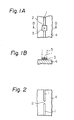
- Figures 1A and 1B illustrate the general principle of the invention.
- a linear aluminum layer 1 is provided on a silicon substrate 4.
- Portion 2 to be cut is coated with an amorphous silicon layer 3 (Fig. lA).
- the reflectivity of aluminum and silicon is 0.92 and 0.41, respectively at wave length of 0.5 ⁇ m.
- the amorphous silicon layer 3 is irradiated by a laser beam 5 (Fig. 1B).
- the laser beam melts the silicon layer 3 and just the portion of the aluminum layer 1 under the silicon layer 3, while leaving the other portions intact. Surface tension then causes the molten aluminum to separate, completing the cut (Fig. 2). During this process, the silicon becomes alloyed with the molten aluminium.
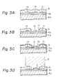
- FIG. 3A An embodiment of the present invention will now be described in detail referring to Figs. 3A to 3D and Figs. 4A and 4B.
- Three linear aluminum layers la.to lc having 1 p m width and spaced 1 ⁇ m from each other are deposited at a thickness of 1 ⁇ m on a silicon dioxide film 4b formed on the silicon substrate 4a.
- a protective phosphorus silicate glass (PSG) film 6 is formed by chemical vapour deposition (Fig. 3A).
- a window 7 is opened in the PSG film 6 by etching it with a mixture of hydrogen fluoride and ammonium fluoride solutions.
- a window 7 is opened in the PSG film 6 by etching it with a mixture of hydrogen fluoride and ammonium fluoride solutions.
- the portion of aluminum layer lb to be cut is exposed (Fig. 3B).
- An amorphous silicon layer 3 is deposited at a thickness of 0.01 to 0.1 ⁇ m (Fig. 3C).
- the layer 3 is then removed, except for the region of aluminum layer lb to be cut, by plasma etching using tetrafluorocarbon (Fig. 3D).
- a continuous wave argon laser beam 5 with an intensity of 9 W having a 5 ⁇ m beam diameter irradiates for 0.1 second the amorphous silicon layer 3, through the window 7, and the PSG film 6 surrounding the window 7 (Figs. 3D, 4A).
- the amorphous silicon layer 3 and the underlying section of the aluminum layer lb melt.
- the aluminum layer lb is then separated at the portion 2 owing to the surface tension of the molten aluminum.
- the other aluminum layers la and lc are not affected by the irradiation of the laser beam (Fig. 4B).
- the amorphous silicon layer 3 is deposited on the aluminum layer lb, whereas the protective PSG film 6 is deposited on the other aluminum layers la and lc (Fig. 3C).
- the protective film is silicon oxynitride (SiON) or polyimide, which can be deposited at a relatively low temperature at which aluminum and amorphous silicon do not alloy with each other, such protective films may be deposited after the amorphous silicon layer is deposited on the aluminum layer.
- polysilicon having higher melting point may be deposited instead of amorphous silicon.
- the present invention enables easy, selective cutting of the electrical conductive layer at the exactly intended portion without damaging other portions, thereby increasing the yield of the products, such as semiconductor devices, and improving the reliability thereof.
Landscapes
- Internal Circuitry In Semiconductor Integrated Circuit Devices (AREA)
- Design And Manufacture Of Integrated Circuits (AREA)
- Semiconductor Memories (AREA)
Abstract
Description
- The present invention relates to a process for selectively cutting an electrical conductive layer by irradiation with an energy beam.
- Increasing integration of elements in semiconductor devices such as a dynamic random access memory has made it desirable not to have to scrap an entire semiconductor chip just because of a failure in one element in the chip. Toward this end, semiconductor chips which include "redundant" circuits have been developed. To salvage a chip found to have a faulty element in one cell, one of the redundant circuits is activated to replace the cell with the faulty element and the circuit which leads to the faulty cell is cut. Selective cutting of an electrical conductive layer has been developed to meet this requirement in the production of random access memories (RAMs), read only memories (ROMs), and other devices.
- It is-well known in the art selectively to cut conductive layers by partial removal of the metallic layer with an etchant or by melting the metallic layer with an excess current. Recently, selective cutting by laser beams has been used. Accurate, selective cutting of a layer can be realised, since scanning of a laser beam can be controlled accurately.
- However, the smallest diameter of a practical laser beam is about 3µm. On the other hand, in an integrated circuit with a high packing desnity, the width of aluminium wirings and the space between them may be no more than 1 4m. Thus, the spot irradiated by a laser beam covers adjacent wirings and so it is not possible to use such a laser beam to cut a single wiring.
- According to this invention a process for selectively cutting an electrical conductive layer by irradiation with an energy beam, includes the steps of depositing, a film of an energy beam absorbing material having a greater energy beam absorbtion than the electrical conductive layer on a portion of the electrical conductive layer to be cut and then irradiating the film with the energy beam, the film absorbing energy from the energy beam and transferring the absorbed energy to the layer thereby melting the portion of the electrical conductive layer.
- This invention enables minute sections of an electrical conductive layer to be cut accurately without damaging regions adjacent the cut portion.
- Preferably the energy beam is.a laser beam. It is convenient when the electrical conductive layer is aluminium for the energy absorbing film to be amorphous silicon, and when the electrical conductive layer is a refractory metal for the heat-absorbing film to be polysilicon or amorphous silicon.
- A particular example of a process in accordance with this invention will now be described with reference to the accompanying drawings; in which:-
- Figure 1A is a plan of an electrical conductive layer, a portion of which is coated with a heat-absorbing material;
- Figure 1B is a section taken along line B-B shown in Figure lA;
- Figure 2 is a plan of a cut electrical conductive layer;
- Figures 3A to 3D are detailed sections illustrating the steps of selective cutting the layers according to'the present invention;
- Figure 4A is a plan of the layers shown in Figure 3D; and,
- Figure 4B is a plan after cutting.
- Figures 1A and 1B illustrate the general principle of the invention. A linear aluminum layer 1 is provided on a
silicon substrate 4.Portion 2 to be cut is coated with an amorphous silicon layer 3 (Fig. lA). The reflectivity of aluminum and silicon is 0.92 and 0.41, respectively at wave length of 0.5 µm. - The
amorphous silicon layer 3 is irradiated by a laser beam 5 (Fig. 1B). The laser beam melts thesilicon layer 3 and just the portion of the aluminum layer 1 under thesilicon layer 3, while leaving the other portions intact. Surface tension then causes the molten aluminum to separate, completing the cut (Fig. 2). During this process, the silicon becomes alloyed with the molten aluminium. - An embodiment of the present invention will now be described in detail referring to Figs. 3A to 3D and Figs. 4A and 4B. Three linear aluminum layers la.to lc having 1 pm width and spaced 1 µm from each other are deposited at a thickness of 1 µm on a
silicon dioxide film 4b formed on thesilicon substrate 4a. A protective phosphorus silicate glass (PSG)film 6 is formed by chemical vapour deposition (Fig. 3A). - A
window 7 is opened in thePSG film 6 by etching it with a mixture of hydrogen fluoride and ammonium fluoride solutions. Thus, the portion of aluminum layer lb to be cut is exposed (Fig. 3B). Anamorphous silicon layer 3 is deposited at a thickness of 0.01 to 0.1 µm (Fig. 3C). Thelayer 3 is then removed, except for the region of aluminum layer lb to be cut, by plasma etching using tetrafluorocarbon (Fig. 3D). A continuous waveargon laser beam 5 with an intensity of 9 W having a 5 µm beam diameter irradiates for 0.1 second theamorphous silicon layer 3, through thewindow 7, and thePSG film 6 surrounding the window 7 (Figs. 3D, 4A). - The
amorphous silicon layer 3 and the underlying section of the aluminum layer lb melt. The aluminum layer lb is then separated at theportion 2 owing to the surface tension of the molten aluminum. On the other hand, the other aluminum layers la and lc are not affected by the irradiation of the laser beam (Fig. 4B). - In the above-mentioned embodiment, the
amorphous silicon layer 3 is deposited on the aluminum layer lb, whereas theprotective PSG film 6 is deposited on the other aluminum layers la and lc (Fig. 3C). In the case where the protective film is silicon oxynitride (SiON) or polyimide, which can be deposited at a relatively low temperature at which aluminum and amorphous silicon do not alloy with each other, such protective films may be deposited after the amorphous silicon layer is deposited on the aluminum layer. - i If refractory metals, such as molybdenum, tungsten, and platinum are used as electrical conductive layers, polysilicon having higher melting point may be deposited instead of amorphous silicon.
- The present invention enables easy, selective cutting of the electrical conductive layer at the exactly intended portion without damaging other portions, thereby increasing the yield of the products, such as semiconductor devices, and improving the reliability thereof.
Claims (4)
Applications Claiming Priority (2)
| Application Number | Priority Date | Filing Date | Title |
|---|---|---|---|
| JP57052100A JPS58169940A (en) | 1982-03-30 | 1982-03-30 | Manufacture of semiconductor device |
| JP52100/82 | 1982-03-30 |
Publications (3)
| Publication Number | Publication Date |
|---|---|
| EP0090565A2 true EP0090565A2 (en) | 1983-10-05 |
| EP0090565A3 EP0090565A3 (en) | 1985-06-19 |
| EP0090565B1 EP0090565B1 (en) | 1989-09-20 |
Family
ID=12905422
Family Applications (1)
| Application Number | Title | Priority Date | Filing Date |
|---|---|---|---|
| EP83301534A Expired EP0090565B1 (en) | 1982-03-30 | 1983-03-18 | Process for selectively cutting an electrical conductive layer by irradiation with an energy beam |
Country Status (4)
| Country | Link |
|---|---|
| US (1) | US4476375A (en) |
| EP (1) | EP0090565B1 (en) |
| JP (1) | JPS58169940A (en) |
| DE (1) | DE3380616D1 (en) |
Cited By (11)
| Publication number | Priority date | Publication date | Assignee | Title |
|---|---|---|---|---|
| EP0189598A1 (en) * | 1984-12-27 | 1986-08-06 | Kabushiki Kaisha Toshiba | Method for manufacturing a semiconductor device |
| EP0208463A1 (en) * | 1985-06-24 | 1987-01-14 | GOVERNMENT OF THE UNITED STATES OF AMERICA as represented by the US department of energy | Planarization of metal films for multilevel interconnects |
| DE3634167A1 (en) * | 1985-10-09 | 1987-04-16 | Mitsubishi Electric Corp | REDUNDANCY CIRCUIT OF A SEMICONDUCTOR DEVICE AND METHOD FOR THE PRODUCTION THEREOF |
| DE3741706A1 (en) * | 1987-12-09 | 1989-06-22 | Asea Brown Boveri | Method for producing spiral thin-film flat coils |
| EP0388341A3 (en) * | 1989-03-14 | 1991-07-17 | International Business Machines Corporation | Method and apparatus for causing an open circuit in a conductive line |
| EP0608764A1 (en) * | 1993-01-21 | 1994-08-03 | Matsushita Electric Industrial Co., Ltd. | Conductor cutting method and coil parts |
| US5374590A (en) * | 1993-04-28 | 1994-12-20 | International Business Machines Corporation | Fabrication and laser deletion of microfuses |
| EP0720229A3 (en) * | 1994-12-29 | 1998-01-07 | Siemens Aktiengesellschaft | Double density fuse bank for the laser break-link programming of an integrated circuit |
| GB2338201A (en) * | 1998-06-13 | 1999-12-15 | Exitech Ltd | Laser drilling of holes in materials |
| FR2921752A1 (en) * | 2007-10-01 | 2009-04-03 | Aplinov Sarl | METHOD FOR HEATING A PLATE BY A LUMINOUS FLOW |
| CN107283075A (en) * | 2017-08-02 | 2017-10-24 | 武汉华星光电半导体显示技术有限公司 | Improve the method for chamfered area defect in laser cutting parameter |
Families Citing this family (17)
| Publication number | Priority date | Publication date | Assignee | Title |
|---|---|---|---|---|
| US4604513A (en) * | 1985-05-07 | 1986-08-05 | Lim Basilio Y | Combination of a laser and a controller for trimming a metallized dielectric film capacitor |
| US4745258A (en) * | 1985-08-27 | 1988-05-17 | Mitsubishi Denki Kabushiki Kaisha | Apparatus for laser-cutting metal interconnections in a semiconductor device |
| US5329152A (en) * | 1986-11-26 | 1994-07-12 | Quick Technologies Ltd. | Ablative etch resistant coating for laser personalization of integrated circuits |
| JPS63262621A (en) * | 1987-04-21 | 1988-10-28 | Alps Electric Co Ltd | Trimming method for thin film transistor array |
| DE3834361A1 (en) * | 1988-10-10 | 1990-04-12 | Lsi Logic Products Gmbh | CONNECTION FRAME FOR A VARIETY OF CONNECTIONS |
| JPH02112890A (en) * | 1988-10-20 | 1990-04-25 | Showa Denko Kk | Method for cutting diamond |
| US5102830A (en) * | 1990-07-24 | 1992-04-07 | Micron Technology, Inc. | Integrated circuit fabrication process for preventing overprocessing during a laser scan |
| JPH05235170A (en) * | 1992-02-24 | 1993-09-10 | Nec Corp | Semiconductor device |
| US5963825A (en) * | 1992-08-26 | 1999-10-05 | Hyundai Electronics America | Method of fabrication of semiconductor fuse with polysilicon plate |
| US5747868A (en) * | 1995-06-26 | 1998-05-05 | Alliance Semiconductor Corporation | Laser fusible link structure for semiconductor devices |
| US5759428A (en) * | 1996-03-15 | 1998-06-02 | International Business Machines Corporation | Method of laser cutting a metal line on an MR head |
| DE19924153B4 (en) * | 1999-05-26 | 2006-02-09 | Infineon Technologies Ag | Circuit arrangement for repair of a semiconductor memory |
| US6650519B1 (en) | 1999-08-17 | 2003-11-18 | Seagate Technology Llc | ESD protection by a high-to-low resistance shunt |
| US6432760B1 (en) * | 2000-12-28 | 2002-08-13 | Infineon Technologies Ag | Method and structure to reduce the damage associated with programming electrical fuses |
| JP2003200279A (en) * | 2001-10-24 | 2003-07-15 | Seiko Epson Corp | Substrate electrical wiring cutting method and apparatus, and electronic device manufacturing method and apparatus |
| JP4006994B2 (en) * | 2001-12-18 | 2007-11-14 | 株式会社リコー | Three-dimensional structure processing method, three-dimensional product manufacturing method, and three-dimensional structure |
| FR2938116B1 (en) * | 2008-11-04 | 2011-03-11 | Aplinov | METHOD AND DEVICE FOR HEATING A LAYER OF A PLATE BY PRIMING AND LUMINOUS FLUX |
Family Cites Families (6)
| Publication number | Priority date | Publication date | Assignee | Title |
|---|---|---|---|---|
| DE2705444A1 (en) * | 1977-02-09 | 1978-08-10 | Siemens Ag | Semiconductor prodn. process using locally limited heating - involves electromagnetic irradiation in specified pulses through mask |
| US4272775A (en) * | 1978-07-03 | 1981-06-09 | National Semiconductor Corporation | Laser trim protection process and structure |
| US4238839A (en) * | 1979-04-19 | 1980-12-09 | National Semiconductor Corporation | Laser programmable read only memory |
| JPS5847596Y2 (en) * | 1979-09-05 | 1983-10-29 | 富士通株式会社 | semiconductor equipment |
| JPS5860560A (en) * | 1981-10-07 | 1983-04-11 | Toshiba Corp | Cutting method for redundant circuit of semiconductor device and fuse part thereof |
| JPS5948543B2 (en) * | 1981-10-13 | 1984-11-27 | 株式会社東芝 | semiconductor equipment |
-
1982
- 1982-03-30 JP JP57052100A patent/JPS58169940A/en active Granted
-
1983
- 1983-03-18 DE DE8383301534T patent/DE3380616D1/en not_active Expired
- 1983-03-18 EP EP83301534A patent/EP0090565B1/en not_active Expired
- 1983-03-25 US US06/478,721 patent/US4476375A/en not_active Expired - Fee Related
Cited By (15)
| Publication number | Priority date | Publication date | Assignee | Title |
|---|---|---|---|---|
| EP0189598A1 (en) * | 1984-12-27 | 1986-08-06 | Kabushiki Kaisha Toshiba | Method for manufacturing a semiconductor device |
| EP0208463A1 (en) * | 1985-06-24 | 1987-01-14 | GOVERNMENT OF THE UNITED STATES OF AMERICA as represented by the US department of energy | Planarization of metal films for multilevel interconnects |
| DE3634167A1 (en) * | 1985-10-09 | 1987-04-16 | Mitsubishi Electric Corp | REDUNDANCY CIRCUIT OF A SEMICONDUCTOR DEVICE AND METHOD FOR THE PRODUCTION THEREOF |
| DE3741706A1 (en) * | 1987-12-09 | 1989-06-22 | Asea Brown Boveri | Method for producing spiral thin-film flat coils |
| EP0388341A3 (en) * | 1989-03-14 | 1991-07-17 | International Business Machines Corporation | Method and apparatus for causing an open circuit in a conductive line |
| US5455389A (en) * | 1993-01-21 | 1995-10-03 | Matsushita Electric Industrial Co., Ltd. | Conductor cutting method and coil parts |
| EP0608764A1 (en) * | 1993-01-21 | 1994-08-03 | Matsushita Electric Industrial Co., Ltd. | Conductor cutting method and coil parts |
| US5374590A (en) * | 1993-04-28 | 1994-12-20 | International Business Machines Corporation | Fabrication and laser deletion of microfuses |
| EP0720229A3 (en) * | 1994-12-29 | 1998-01-07 | Siemens Aktiengesellschaft | Double density fuse bank for the laser break-link programming of an integrated circuit |
| GB2338201A (en) * | 1998-06-13 | 1999-12-15 | Exitech Ltd | Laser drilling of holes in materials |
| FR2921752A1 (en) * | 2007-10-01 | 2009-04-03 | Aplinov Sarl | METHOD FOR HEATING A PLATE BY A LUMINOUS FLOW |
| WO2009050381A3 (en) * | 2007-10-01 | 2009-06-11 | Aplinov | Method for heating a plate with a light stream |
| US8324530B2 (en) | 2007-10-01 | 2012-12-04 | Soitec | Method for heating a wafer by means of a light flux |
| CN107283075A (en) * | 2017-08-02 | 2017-10-24 | 武汉华星光电半导体显示技术有限公司 | Improve the method for chamfered area defect in laser cutting parameter |
| CN107283075B (en) * | 2017-08-02 | 2019-01-15 | 武汉华星光电半导体显示技术有限公司 | Improve the method for chamfered area defect in laser cutting parameter |
Also Published As
| Publication number | Publication date |
|---|---|
| US4476375A (en) | 1984-10-09 |
| JPS6412095B2 (en) | 1989-02-28 |
| DE3380616D1 (en) | 1989-10-26 |
| EP0090565B1 (en) | 1989-09-20 |
| JPS58169940A (en) | 1983-10-06 |
| EP0090565A3 (en) | 1985-06-19 |
Similar Documents
| Publication | Publication Date | Title |
|---|---|---|
| EP0090565B1 (en) | Process for selectively cutting an electrical conductive layer by irradiation with an energy beam | |
| EP0162145B1 (en) | Method of melting a fuse using a laser beam | |
| EP0083211B1 (en) | Semiconductor device with fuse | |
| US4665295A (en) | Laser make-link programming of semiconductor devices | |
| US6521971B2 (en) | Metal fuse in copper dual damascene | |
| US4912066A (en) | Make-link programming of semiconductor devices using laser-enhanced thermal breakdown of insulator | |
| US4748491A (en) | Redundant circuit of semiconductor device and method of producing same | |
| US4968643A (en) | Method for fabricating an activatable conducting link for metallic conductive wiring in a semiconductor device | |
| KR920000227B1 (en) | Redundancy Circuit of Semiconductor Device | |
| US5936297A (en) | Programmable semiconductor element having an antifuse structure | |
| US5100834A (en) | Method of planarizing metal layer | |
| EP0189598B1 (en) | Method for manufacturing a semiconductor device | |
| JP3489088B2 (en) | Semiconductor device having redundant means and method of manufacturing the same | |
| EP0999592B1 (en) | Fuse layout for improved fuse blow process window | |
| US5235154A (en) | Laser removal of metal interconnects | |
| JP2793232B2 (en) | Semiconductor device suitable for cutting and connecting wiring by ion beam | |
| JPS6193643A (en) | Semiconductor programmable with laser beam and manufacture thereof | |
| JPS6084837A (en) | Semiconductor integrated circuit device | |
| JPH09172087A (en) | Semiconductor device | |
| US20050205965A1 (en) | Semiconductor device having a fuse including an aluminum layer | |
| JPH05166935A (en) | Semiconductor device and manufacturing method thereof | |
| JPS6122652A (en) | Semiconductor device | |
| JPH1050852A (en) | Method for manufacturing semiconductor device | |
| JPH0616536B2 (en) | Semiconductor device having fuse ROM and method of conducting fuse ROM | |
| JPH079942B2 (en) | Method of connecting a conductor to a doped region of a substrate of an integrated circuit by a laser, and an integrated circuit obtained by implementing the method |
Legal Events
| Date | Code | Title | Description |
|---|---|---|---|
| PUAI | Public reference made under article 153(3) epc to a published international application that has entered the european phase |
Free format text: ORIGINAL CODE: 0009012 |
|
| AK | Designated contracting states |
Designated state(s): DE FR GB |
|
| PUAL | Search report despatched |
Free format text: ORIGINAL CODE: 0009013 |
|
| AK | Designated contracting states |
Designated state(s): DE FR GB |
|
| 17P | Request for examination filed |
Effective date: 19851202 |
|
| 17Q | First examination report despatched |
Effective date: 19870327 |
|
| GRAA | (expected) grant |
Free format text: ORIGINAL CODE: 0009210 |
|
| AK | Designated contracting states |
Kind code of ref document: B1 Designated state(s): DE FR GB |
|
| REF | Corresponds to: |
Ref document number: 3380616 Country of ref document: DE Date of ref document: 19891026 |
|
| ET | Fr: translation filed | ||
| PLBE | No opposition filed within time limit |
Free format text: ORIGINAL CODE: 0009261 |
|
| STAA | Information on the status of an ep patent application or granted ep patent |
Free format text: STATUS: NO OPPOSITION FILED WITHIN TIME LIMIT |
|
| 26N | No opposition filed | ||
| PGFP | Annual fee paid to national office [announced via postgrant information from national office to epo] |
Ref country code: FR Payment date: 19911231 Year of fee payment: 10 |
|
| PGFP | Annual fee paid to national office [announced via postgrant information from national office to epo] |
Ref country code: GB Payment date: 19920311 Year of fee payment: 10 |
|
| PGFP | Annual fee paid to national office [announced via postgrant information from national office to epo] |
Ref country code: DE Payment date: 19920522 Year of fee payment: 10 |
|
| PG25 | Lapsed in a contracting state [announced via postgrant information from national office to epo] |
Ref country code: GB Effective date: 19930318 |
|
| GBPC | Gb: european patent ceased through non-payment of renewal fee |
Effective date: 19930318 |
|
| PG25 | Lapsed in a contracting state [announced via postgrant information from national office to epo] |
Ref country code: FR Effective date: 19931130 |
|
| PG25 | Lapsed in a contracting state [announced via postgrant information from national office to epo] |
Ref country code: DE Effective date: 19931201 |
|
| REG | Reference to a national code |
Ref country code: FR Ref legal event code: ST |