EP0090634A2 - Mehrschichtkondensatoren mit keramischen Dielektrikum - Google Patents
Mehrschichtkondensatoren mit keramischen Dielektrikum Download PDFInfo
- Publication number
- EP0090634A2 EP0090634A2 EP83301739A EP83301739A EP0090634A2 EP 0090634 A2 EP0090634 A2 EP 0090634A2 EP 83301739 A EP83301739 A EP 83301739A EP 83301739 A EP83301739 A EP 83301739A EP 0090634 A2 EP0090634 A2 EP 0090634A2
- Authority
- EP
- European Patent Office
- Prior art keywords
- metal
- silver
- lead
- pseudo
- ceramic powder
- Prior art date
- Legal status (The legal status is an assumption and is not a legal conclusion. Google has not performed a legal analysis and makes no representation as to the accuracy of the status listed.)
- Withdrawn
Links
Images
Classifications
-
- H—ELECTRICITY
- H01—ELECTRIC ELEMENTS
- H01G—CAPACITORS; CAPACITORS, RECTIFIERS, DETECTORS, SWITCHING DEVICES, LIGHT-SENSITIVE OR TEMPERATURE-SENSITIVE DEVICES OF THE ELECTROLYTIC TYPE
- H01G4/00—Fixed capacitors; Processes of their manufacture
- H01G4/002—Details
- H01G4/228—Terminals
- H01G4/232—Terminals electrically connecting two or more layers of a stacked or rolled capacitor
- H01G4/2325—Terminals electrically connecting two or more layers of a stacked or rolled capacitor characterised by the material of the terminals
-
- Y—GENERAL TAGGING OF NEW TECHNOLOGICAL DEVELOPMENTS; GENERAL TAGGING OF CROSS-SECTIONAL TECHNOLOGIES SPANNING OVER SEVERAL SECTIONS OF THE IPC; TECHNICAL SUBJECTS COVERED BY FORMER USPC CROSS-REFERENCE ART COLLECTIONS [XRACs] AND DIGESTS
- Y10—TECHNICAL SUBJECTS COVERED BY FORMER USPC
- Y10T—TECHNICAL SUBJECTS COVERED BY FORMER US CLASSIFICATION
- Y10T29/00—Metal working
- Y10T29/43—Electric condenser making
- Y10T29/435—Solid dielectric type
Definitions
- This invention relates to electrical components such as multilayer ceramic dielectric capacitors and in particular, but not exclusively, to metal-impregnated- electrode multilayer-ceramic-dielectric capacitors.
- an electrical solderable connection termination in an electrical component comprising forming on an exposed surface of the component a very porous pseudo termination in which the pores are lead wettable, and impregnating the pseudo termination with lead or a lead alloy to produce the solderable connection termination.
- a method of manufacturing an electrical solderable connection termination in an electrical component comprising forming a porous pseudo termination on the component substrate by firing a frit containing glass and a coarse ceramic powder thereon, the ceramic powder having a coating of a first metal, and impregnating the pseudo termination with a second metal whereby to provide a connection termination comprised by the second metal held in place by the fired-on ceramic powder,
- a method of manufacturing a multilayer ceramic dielectric capacitor including the steps of applying a frit containing glass and a coarse ceramic powder, having a coating of a first metal, to end faces of the capacitor to which electrodes of the capacitor extend, firing the frit to provide pseudo end terminations and impregnating the pseudo end terminations with a second metal to provide end terminations in contact with the capacitor electrodes and comprised by the second metal held in place by the fired-on ceramic powder.
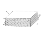
- the basic capacitor comprises a stack of ceramic dielectric layers 1 with electrodes 2a and 2b therebetween.
- Alternate electrodes 2a terminate at the right hand face 3 and do not extend completely to the left hand face 4, whereas alternate electrodes 2b extend to the left hand face 4, but do not reach the right hand face 3.
- the electrodes 2b can be electrically interconnected at the end face 4 (end terminated) and the electrodes 2a can be likewise electrically interconnected at the end face 3, to form two electrically insulated sets of electrodes 2a and 2h.
- the electrode sets are shown as extending to the lateral sides of the stack. However, in practice neither set of electrodes extend to the lateral sides, which in the finished device are all ceramic.
- the internal electrodes 2a and 2b may alternatively, for example, have elongate portions which cross cne another, as described in our co-pending Application No. 41677/78 (Serial No. 2032683) (A.L.Qliver-G.Mills 1-1), or instead of being rectangular the electrodes may be comprised of pluralities of parallel conductive lines, as described in our co-pending British Appllcation No.82Q4777 (Serial No. ) (J.H.Alexander 21).
- the manufacture of multilayer-ceramic-dielectric capacitors with the basic structure shown in the drawing comprises the following steps.
- Green (unfired) ceramic sheets of barium titanate, for example, are prepared in a conventional manner, for example tape casting, tape drawing or printing.
- a screen-printing technique is employed to print a large number of electrodes side by side on one relatively large sheet of green ceramic, although alternatively a single electrode may be provided on a suitably sized sheet of green ceramic.
- the electrodes may be printed by means of a conductive ink or, in the case of metal-impregnated electrodes, the printed electrodes on the green ceramic comprise fugitive electrodes printed by means of a fugitive electrode ink comprising a charcoal powder with a binder and solvent such as to make it compatible with the green ceramic. Further sheets are similarly printed. A number of such sheets, the number corresponding to the number of electrodes in each c-apacitor, are stacked one on top of the other with the electrodes staggered and partially overlying one another as illustrated in the drawing. A blank green ceramic sheet is applied to the top of the stack. Extra blank green ceramic sheets may be applied to the top and bottom of the stack in order to protect the outer electrodes and to give adequate strength to the finished device.
- the block Q f stacked green ceramic sheets thus formed is cut to make individual green capacitor elements. The electrodes do not extend up to the lateral cut faces as previously mentioned.
- the capacitors are fired.
- the green capacitor elements are heated at for example, 1 C/min to 350°C, to bake out the binders in the fugitive ink and the green ceramic, before firing at, for example, 200°C/hour to 1120°C for 2 hours in a conventional manner, during which firing the charcoal of the fugitive ink burns, providing spaces between the dielectric layers comprised by the fired ceramic sheets which become sealed together during the firing process.
- the fired capacitor elements are then end terminated at faces 3 and 4 whereby to connect the alternate electrodes 2a and 2b of the drawing, or in the case of fugitive electrodes, to connect the alternate spaces between the dielectric layers.
- the illustrated gaps at the end faces 3 and 4 provided by the staggered overlying arrangement of the electrodes being closed by ceramic of the dielectric layers 1 during the manufacturing process.
- the lateral faces are closed by ceramic.
- end terminations of multilayer ceramic capacitors in particular fugitive electrode (lead-impregnated) capacitors, are conventionally formed from precious metals such as silver or silver/palladium mixtures. These metals are used as fine powders and are bonded to the ceramic by firing on together with glass frits. Such terminations are expensive, in view of the precious metal content, and subject to silver leaching by the lead of lead impregnated capacitors. Whilst we have successfully used aluminium and aluminium/silver terminations in an attempt to solve the dissolution problem and provide cheaper end terminations, as is described for example in our co-pending British Application No. 8203644 (Serial No.
- silver/glass frit terminations can be treated such as to overcome the dissolution problem and solderability problem in one step. This is accomplished by lightly sulphiding the silver of silver/glass frit terminations as is described in our co-pending European Application No. (Serial No. ) (J.H.Alexander 22). In the case of lead impregnated capacitors, the silver sulphide layer formed on the silver provides a barrier between the lead and the silver which prevents silver leaching by the lead, and the lead wets the silver sulphide layer to provide a lead layer thereon which renders the termination readily solderable. These sulphided terminations still include a high proportion of silver and are thus expensive to produce.
- the terminations of the present invention are made by lightly coating the surfaces of ceramic powders, such as alumina Al 2 O 3 , silica, SiO 2 , for example, with silver.
- the silver-coated ceramic powder is then mixed with a glass frit and made into a termination paste which is applied to a capacitor, or other suitable electrical component, such as film circuits, in a conventional manner and fired to bond it thereto at a temperature of the order of, for example, 700°C.
- the firing temperature is dependent on the glass frit used and may be in the range 500-800°C.
- the end terminations thus formed contain so little silver that they do not conduct enough to give a good contact with the electrodes of the capacitor, and are thus termed "pseudo end terminations".
- the exposed silver coating on the pseudo end terminations is then lightly sulphided. This may be accomplished by heating the capacitors to 350-400°C in a chamber that can be evacuated to remove air from the voids in the pseudo end terminations and the capacitors and subsequently admitting small quantities of hydrogen sulphide or sulphur vapour, for example, into the evacuated chamber where it forms silver sulphide Ag 2 S on contact with the silver.
- the capacitors are then transferred to lead impregnation equipment where air is evacuated from voids in the capacitors, which are then immersed in molten lead that is forced into the pseudo end terminations by nitrogen under pressure, whereby the terminations become filled with and coated by lead.
- the end terminations thus formed are comprised substantially by lead which is held in place by the fritted ceramic powder.
- the silver and silver sulphide coating processes serve to ensure that the lead is held to the ceramic powder by virtue of the lead wetting the silver sulphide layer.
- the end terminations thus formed are readily solderable, whereby to facilitate, for example, the soldering of connection wires thereto. There are no silver leaching problems resulting in lack of end terminations, in view of the low proportion of silver employed and the barrier effect provided by the silver sulphide layer.
- the ceramic powder employed are necessarily of a relatively coarse nature such that the pseudo end terminations are very porous in order to facilitate the sulphiding and lead impregnation steps.
- the ceramic powders may be coated with silver in solution. Typically the silver coating is of the order of O ⁇ l/-O.3 ⁇ m thick, and the ceramic powders are of 20-50 ⁇ m particle size.
- the sulphiding agents may alternatively comprise organic materials such as CH 3 SH, C 2 H 5 SH, for example.
Landscapes
- Engineering & Computer Science (AREA)
- Power Engineering (AREA)
- Manufacturing & Machinery (AREA)
- Microelectronics & Electronic Packaging (AREA)
- Ceramic Capacitors (AREA)
- Fixed Capacitors And Capacitor Manufacturing Machines (AREA)
Applications Claiming Priority (2)
| Application Number | Priority Date | Filing Date | Title |
|---|---|---|---|
| GB08209285A GB2119571B (en) | 1982-03-30 | 1982-03-30 | Terminals for multilayer ceramic dielectric capacitors |
| GB8209285 | 1982-03-30 |
Publications (2)
| Publication Number | Publication Date |
|---|---|
| EP0090634A2 true EP0090634A2 (de) | 1983-10-05 |
| EP0090634A3 EP0090634A3 (de) | 1985-05-22 |
Family
ID=10529390
Family Applications (1)
| Application Number | Title | Priority Date | Filing Date |
|---|---|---|---|
| EP83301739A Withdrawn EP0090634A3 (de) | 1982-03-30 | 1983-03-29 | Mehrschichtkondensatoren mit keramischen Dielektrikum |
Country Status (4)
| Country | Link |
|---|---|
| US (1) | US4455590A (de) |
| EP (1) | EP0090634A3 (de) |
| JP (1) | JPS58207615A (de) |
| GB (1) | GB2119571B (de) |
Cited By (2)
| Publication number | Priority date | Publication date | Assignee | Title |
|---|---|---|---|---|
| FR2568053A1 (fr) * | 1984-07-23 | 1986-01-24 | Avx Corp | Procede de fabrication d'un condensateur ceramique multicouche et condensateur ainsi obtenu |
| US11152155B2 (en) * | 2018-10-29 | 2021-10-19 | Samsung Electro-Mechanics Co., Ltd. | Capacitor component having secondary phase material contained in external electrode thereof |
Families Citing this family (7)
| Publication number | Priority date | Publication date | Assignee | Title |
|---|---|---|---|---|
| US4791006A (en) * | 1987-06-04 | 1988-12-13 | Avx Corporation | High accuracy variable thickness laydown method for electronic components |
| AT391770B (de) * | 1987-07-31 | 1990-11-26 | Siemens Bauelemente Ohg | Elektrisches vielschichtbauelement mit einem gesinterten, monolithischen keramikkoerper und verfahren zur herstellung des elektrischen vielschichtbauelementes |
| US4881308A (en) * | 1988-07-01 | 1989-11-21 | Avx Corporation | Method of terminating lead filled capacitor |
| JP2872446B2 (ja) * | 1991-06-10 | 1999-03-17 | ローム株式会社 | 積層セラミックコンデンサ |
| US5495386A (en) * | 1993-08-03 | 1996-02-27 | Avx Corporation | Electrical components, such as capacitors, and methods for their manufacture |
| US6819540B2 (en) * | 2001-11-26 | 2004-11-16 | Shipley Company, L.L.C. | Dielectric structure |
| US20130026425A1 (en) * | 2011-07-29 | 2013-01-31 | Giga Solar Materials Corporation | Conductive Composition and Method for Manufacturing |
Family Cites Families (9)
| Publication number | Priority date | Publication date | Assignee | Title |
|---|---|---|---|---|
| DE1639554B1 (de) * | 1961-07-01 | 1969-12-04 | Meinhard Dipl-Phys Bethe | Elektrischer Kondensator hoher Kapazitaetsdichte und Verfahren zu seiner Herstellung |
| US3237066A (en) * | 1963-02-25 | 1966-02-22 | Sprague Electric Co | Capacitor with electrodes of metal coated particles |
| US3755723A (en) * | 1968-02-26 | 1973-08-28 | Du Pont | Novel glasses, silver compositions and capacitors therefrom |
| US3604082A (en) * | 1968-10-30 | 1971-09-14 | Corning Glass Works | Method of making a capacitor |
| US3612963A (en) * | 1970-03-11 | 1971-10-12 | Union Carbide Corp | Multilayer ceramic capacitor and process |
| IL41904A (en) * | 1972-07-24 | 1976-03-31 | Nl Industries Inc | Sintered ceramic bodies for use as electrical components and their manufacture |
| US3965552A (en) * | 1972-07-24 | 1976-06-29 | N L Industries, Inc. | Process for forming internal conductors and electrodes |
| JPS5212452A (en) * | 1975-07-18 | 1977-01-31 | Taiyo Yuden Kk | Ceramic capacitor |
| JPS5225253A (en) * | 1975-08-21 | 1977-02-25 | Murata Manufacturing Co | Method of manufacturing laminated ceramic capacitor |
-
1982
- 1982-03-30 GB GB08209285A patent/GB2119571B/en not_active Expired
-
1983
- 1983-02-17 US US06/467,533 patent/US4455590A/en not_active Expired - Fee Related
- 1983-03-29 JP JP58053465A patent/JPS58207615A/ja active Pending
- 1983-03-29 EP EP83301739A patent/EP0090634A3/de not_active Withdrawn
Cited By (2)
| Publication number | Priority date | Publication date | Assignee | Title |
|---|---|---|---|---|
| FR2568053A1 (fr) * | 1984-07-23 | 1986-01-24 | Avx Corp | Procede de fabrication d'un condensateur ceramique multicouche et condensateur ainsi obtenu |
| US11152155B2 (en) * | 2018-10-29 | 2021-10-19 | Samsung Electro-Mechanics Co., Ltd. | Capacitor component having secondary phase material contained in external electrode thereof |
Also Published As
| Publication number | Publication date |
|---|---|
| GB2119571A (en) | 1983-11-16 |
| EP0090634A3 (de) | 1985-05-22 |
| JPS58207615A (ja) | 1983-12-03 |
| US4455590A (en) | 1984-06-19 |
| GB2119571B (en) | 1985-12-11 |
Similar Documents
| Publication | Publication Date | Title |
|---|---|---|
| EP0100175B1 (de) | Chip-Kondensator mit biegsamem Anschluss | |
| CN113593906B (zh) | 陶瓷电子部件以及陶瓷电子部件的制造方法 | |
| JP7562249B2 (ja) | セラミック電子部品およびその製造方法 | |
| JP2992570B2 (ja) | セラミック多層コンデンサおよびその製造方法 | |
| EP0412259B1 (de) | Elektronische Verbindungen, Verfahren zur Bildung von Endverbindern dafür und Paste zur Ausbildung derselben | |
| US4953273A (en) | Process for applying conductive terminations to ceramic components | |
| US4455590A (en) | Multilayer ceramic dielectric capacitors | |
| JP2943380B2 (ja) | 積層セラミックコンデンサとその製造方法 | |
| US4470098A (en) | Multilayer ceramic dielectric capacitors | |
| JP2970030B2 (ja) | 積層セラミックコンデンサとその製造方法およびそれに用いる外部電極用ペースト | |
| GB2110878A (en) | Batch process for making capacitors | |
| US4956744A (en) | Multilayer capacitor | |
| US4450502A (en) | Multilayer ceramic dielectric capacitors | |
| JP3120703B2 (ja) | 導電性ペースト及び積層セラミック電子部品 | |
| JPH08330173A (ja) | 積層セラミックコンデンサならびにその製造方法 | |
| EP0072126A2 (de) | Mehrlagige Kondensatoren mit Keramikdielektrikum | |
| KR100807217B1 (ko) | 세라믹 부품 및 그 제조방법 | |
| JPH0348415A (ja) | ペースト組成物および積層セラミックコンデンサの製造方法 | |
| JPH07201637A (ja) | 積層セラミック電子部品 | |
| JPH0494517A (ja) | 積層インダクタの製造方法 | |
| JPH03191596A (ja) | コンデンサ内蔵多層セラミック基板の製造方法 | |
| JP2002313664A (ja) | 導電性ペーストおよび積層セラミック電子部品 | |
| JP3485328B2 (ja) | 積層型部品の製造方法 | |
| JPH0729769A (ja) | セラミック電子部品 | |
| JPH04105310A (ja) | 積層セラミックコンデンサ |
Legal Events
| Date | Code | Title | Description |
|---|---|---|---|
| PUAI | Public reference made under article 153(3) epc to a published international application that has entered the european phase |
Free format text: ORIGINAL CODE: 0009012 |
|
| AK | Designated contracting states |
Designated state(s): DE FR IT SE |
|
| PUAL | Search report despatched |
Free format text: ORIGINAL CODE: 0009013 |
|
| AK | Designated contracting states |
Designated state(s): DE FR IT SE |
|
| 17P | Request for examination filed |
Effective date: 19850409 |
|
| RAP1 | Party data changed (applicant data changed or rights of an application transferred) |
Owner name: STC PLC |
|
| RAP1 | Party data changed (applicant data changed or rights of an application transferred) |
Owner name: STC PLC |
|
| STAA | Information on the status of an ep patent application or granted ep patent |
Free format text: STATUS: THE APPLICATION IS DEEMED TO BE WITHDRAWN |
|
| 18D | Application deemed to be withdrawn |
Effective date: 19861001 |
|
| RIN1 | Information on inventor provided before grant (corrected) |
Inventor name: ALEXANDER, JOHN HENRY |