EP0090669A2 - Détecteur de radiation électromagnétique - Google Patents
Détecteur de radiation électromagnétique Download PDFInfo
- Publication number
- EP0090669A2 EP0090669A2 EP83301844A EP83301844A EP0090669A2 EP 0090669 A2 EP0090669 A2 EP 0090669A2 EP 83301844 A EP83301844 A EP 83301844A EP 83301844 A EP83301844 A EP 83301844A EP 0090669 A2 EP0090669 A2 EP 0090669A2
- Authority
- EP
- European Patent Office
- Prior art keywords
- layer
- detector
- semiconductor
- minority carriers
- semiconductor device
- Prior art date
- Legal status (The legal status is an assumption and is not a legal conclusion. Google has not performed a legal analysis and makes no representation as to the accuracy of the status listed.)
- Withdrawn
Links
Images
Classifications
-
- H—ELECTRICITY
- H10—SEMICONDUCTOR DEVICES; ELECTRIC SOLID-STATE DEVICES NOT OTHERWISE PROVIDED FOR
- H10F—INORGANIC SEMICONDUCTOR DEVICES SENSITIVE TO INFRARED RADIATION, LIGHT, ELECTROMAGNETIC RADIATION OF SHORTER WAVELENGTH OR CORPUSCULAR RADIATION
- H10F77/00—Constructional details of devices covered by this subclass
- H10F77/10—Semiconductor bodies
- H10F77/12—Active materials
- H10F77/124—Active materials comprising only Group III-V materials, e.g. GaAs
- H10F77/1248—Active materials comprising only Group III-V materials, e.g. GaAs having three or more elements, e.g. GaAlAs, InGaAs or InGaAsP
-
- H—ELECTRICITY
- H10—SEMICONDUCTOR DEVICES; ELECTRIC SOLID-STATE DEVICES NOT OTHERWISE PROVIDED FOR
- H10D—INORGANIC ELECTRIC SEMICONDUCTOR DEVICES
- H10D64/00—Electrodes of devices having potential barriers
- H10D64/01—Manufacture or treatment
- H10D64/011—Manufacture or treatment of electrodes ohmically coupled to a semiconductor
-
- H—ELECTRICITY
- H10—SEMICONDUCTOR DEVICES; ELECTRIC SOLID-STATE DEVICES NOT OTHERWISE PROVIDED FOR
- H10F—INORGANIC SEMICONDUCTOR DEVICES SENSITIVE TO INFRARED RADIATION, LIGHT, ELECTROMAGNETIC RADIATION OF SHORTER WAVELENGTH OR CORPUSCULAR RADIATION
- H10F30/00—Individual radiation-sensitive semiconductor devices in which radiation controls the flow of current through the devices, e.g. photodetectors
- H10F30/10—Individual radiation-sensitive semiconductor devices in which radiation controls the flow of current through the devices, e.g. photodetectors the devices being sensitive to infrared radiation, visible or ultraviolet radiation, and having no potential barriers, e.g. photoresistors
-
- H—ELECTRICITY
- H10—SEMICONDUCTOR DEVICES; ELECTRIC SOLID-STATE DEVICES NOT OTHERWISE PROVIDED FOR
- H10F—INORGANIC SEMICONDUCTOR DEVICES SENSITIVE TO INFRARED RADIATION, LIGHT, ELECTROMAGNETIC RADIATION OF SHORTER WAVELENGTH OR CORPUSCULAR RADIATION
- H10F30/00—Individual radiation-sensitive semiconductor devices in which radiation controls the flow of current through the devices, e.g. photodetectors
- H10F30/20—Individual radiation-sensitive semiconductor devices in which radiation controls the flow of current through the devices, e.g. photodetectors the devices having potential barriers, e.g. phototransistors
- H10F30/21—Individual radiation-sensitive semiconductor devices in which radiation controls the flow of current through the devices, e.g. photodetectors the devices having potential barriers, e.g. phototransistors the devices being sensitive to infrared, visible or ultraviolet radiation
- H10F30/22—Individual radiation-sensitive semiconductor devices in which radiation controls the flow of current through the devices, e.g. photodetectors the devices having potential barriers, e.g. phototransistors the devices being sensitive to infrared, visible or ultraviolet radiation the devices having only one potential barrier, e.g. photodiodes
- H10F30/222—Individual radiation-sensitive semiconductor devices in which radiation controls the flow of current through the devices, e.g. photodetectors the devices having potential barriers, e.g. phototransistors the devices being sensitive to infrared, visible or ultraviolet radiation the devices having only one potential barrier, e.g. photodiodes the potential barrier being a PN heterojunction
-
- H—ELECTRICITY
- H10—SEMICONDUCTOR DEVICES; ELECTRIC SOLID-STATE DEVICES NOT OTHERWISE PROVIDED FOR
- H10F—INORGANIC SEMICONDUCTOR DEVICES SENSITIVE TO INFRARED RADIATION, LIGHT, ELECTROMAGNETIC RADIATION OF SHORTER WAVELENGTH OR CORPUSCULAR RADIATION
- H10F77/00—Constructional details of devices covered by this subclass
- H10F77/10—Semiconductor bodies
- H10F77/12—Active materials
- H10F77/123—Active materials comprising only Group II-VI materials, e.g. CdS, ZnS or HgCdTe
- H10F77/1237—Active materials comprising only Group II-VI materials, e.g. CdS, ZnS or HgCdTe having at least three elements, e.g. HgCdTe
Definitions
- the present invention relates generally to semiconductor electromagnetic radiation detectors.
- Photosensitive semiconductors are basically of two types, photoconductive and photovoltaic. When radiation of the proper energy falls upon a photoconductive semiconductor, the conductivity of the semiconductor increases. Energy supplied to the semiconductor causes covalent bonds to be broken, and electron-hole pairs in excess of those generated thermally are created. These increased current carriers decrease the resistance of the material. This "photoconductive effect" in semiconductor materials is used in photoconductive detectors.
- the semiconductor sensor is such that it incorporates a pn junction, it gives rise to electron-hole pairs which create a potential difference in response to radiation of the proper energy. This is referred to as a "photovoltaic" effect.
- the semiconductor electromagnetic radiation detectors which we are concerned with are photoconductive detectors.
- a photoconductive detector can be a bar of semiconductor material having electrical contacts at the ends.
- the photoconductive detector is connected in series with a direct-current voltage source and a load resistor. The change in resistivity of the photoconductive detector in response to incident radiation is sensed.
- the prior art teaches methods to reduce the rate of annihilation of the minority carriers within the detector bulk.
- One well known method for detectors of visible radiation is to incorporate impurities or lattice defects into the detector material which act to temporarily trap the minority carriers and thus reduce the rate of annihilation. Such a technique is described in R.B. Bube, "Photoconductivity of Solids” New York (1960), at p.69.
- the prior art has provided means for improving the responsivity of infrared detectors by reducing the rate of annihilation of minority carriers within the bulk of the infrared detector materials, and by preventing annihilation of minority carriers at surfaces of the detector that are not used for making electrical contacts to the detector.
- the prior art has further disclosed means of prolonging the lifetime of the minority carrier by using a geometry in which the electrical contacts are placed at an increased distance from the absorbed incident radiation.
- an improved semiconductor device comprising a substrate; a first layer on said substrate of electromagnetic radiation sensitive semiconductor material of a given conductivity type and having a first energy bandgap; and at least one ohmic contact for providing electrical communication with said first layer; characterized by a second layer of semiconductor material of the same conductivity type as said first layer but having a second energy bandgap greater than said first energy bandgap, said second layer being located on said first layer beneath the or each ohmic contact to which minority carriers are attracted from said first layer.
- Infrared detectors include a class of materials with energy bandgaps in the range of infrared radiation, typically below 0.8 electron volts. This class includes, for example, materials such as InAs x Sb 1-x , In x Ga 1-x Sb, PbS 1-x Sn x Te, and Hg1 Cd Te, where the quantity x is a number between 0 and 1 as appropriate to the properties desired. This class of detectors is referred to as "intrinsic" detectors.
- a second class of infrared detectors have larger energy bandgaps, but are doped with or have impurities added to provide sensitivity to infrared radiation.
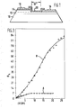
- both the layer 12 and the layer 14 may be formed by a growth process in which a thin layer is grown by liquid phase epitaxy onto the detector substrate material 10. Subsequently, a metal layer 16, compatible with and known to form an ohmic contact to either layer 12 or 14, is deposited as a thin layer onto the surface of layers 12 and 14 in the desired geometry to form the electrical contacts. The photoactive areas beneath the arrow at 18 may be provided with a thin surface passivation layer 20. Finally metal wires, not shown, are bonded to metal layers 16.
- This layer ultimately formed the photosensitive layer of the detector and was approximately 10- 3 cm in thickness.
- a second thin layer 14 was grown on the first layer by similar techniques. The second layer reflected a small change in composition toward a higher bandgap alloy and was doped to the same concentration as the photosensitive layer.
- an overlayer 14 of composition Hg 0.78 Cd 0.22 Te was used in one embodiment.
- the photoconductor structure now included a top layer 14 of wider bandgap material approximately 5 microns in thickness.
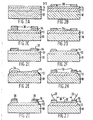
- the surface was then solvent cleaned in a well-known manner and then pretreated with HMDS (hexamethyldisilizane) to promote surface adhesion followed by a photolithographic step ( Figure 2B) using the photoresist material SC100 (Hunt Chemical).
- HMDS hexamethyldisilizane
- SC100 Heunt Chemical
- the first photolithographic step protected areas 30 on the wafer for delineation of the contacts.
- the photoresist was then exposed and developed HMDS (hexamethyldisilizane) to promote surface adhesion followed by a photolithographic step (Figure 2B) using the photoresist material SC100 (Hunt Chemical).
- the first photolithographic step protected areas 30 on the wafer for delineation of the contacts.
- the photoresist was then exposed and developed leaving the resist in the geometry of the particular areas designated for the blocking contacts.
- the wafer was coated at 32 with photoresist SC450 (Hunt Chemical) exposed and developed.
- the developed photoresist was then etched and dipped in a 1% Br-methanol rinse.
- the photoresist was stripped away by plasma stripping. This left the structure of Figure 2F wherein the photosensitive layer 12 remained only in the area between the contacts.
- photoresist AZ1375 was applied and allowed to dry in a dry box. The photoresist was exposed, developed and rinsed. Subsequent to this an additional layer of photoresist AZ1470 was applied, baked, exposed and developed.
- the entire photoconductive device was covered with a layer of photoresist shown at 34 except for the contact areas which were opened up for deposition of metal for ohmic contacts.
- Approximately 0 3300 A of indium were evaporated onto the surface, followed by soaking in acetone to accomplish metal lift-off. This left a layer of indium at the points of desired ohmic contact, as illustrated by Figure 2H.
- both ohmic contacts calls for both ohmic contacts to be supplied with a higher bandgap layer 14 beneath the ohmic contact.
- passivation occurs only for the contact attracting the minority carriers, in this case the holes of the hole-electron pairs and therefore passivation is not necessary under both of the contacts. Because the input of majority carriers is not impeded by the layer 14, however, placing the layers under both contacts appears to be preferred, as it facilitates fabrication and use of the device.
- other variations are contemplated in the process in accordance with the practices of those skilled in-the art.
- R ⁇ is an enormous increase in R ⁇ is observed when the contact that is negatively biased includes the second higher bandgap layer (i.e. when it is blocking) compared to when the contact that is negatively biased does not include the second higher bandgap layer (i.e. when it is ohmic).
- the saturation of R ⁇ occurs at about 7 kV/W for the lower curve (A) at low bias fields. This indicates that sweepout has occurred at low fields for a detector with conventional ohmic contacts.
- R ⁇ is greater than 70 kV/W and still increasing.
- an infrared detector may be processed so as to reduce the rate of recombination of the minority current carriers at the electrical contacts, without either impeding the flow of majority current carriers or significantly increasing the average carrier concentration of the semiconductor material since the barrier to minority carriers does not require increased majority carrier conen- tration. In turn, this increases the lifetime of the minority carriers, which then increases the detector responsivity.
Landscapes
- Light Receiving Elements (AREA)
Applications Claiming Priority (2)
| Application Number | Priority Date | Filing Date | Title |
|---|---|---|---|
| US36398082A | 1982-03-31 | 1982-03-31 | |
| US363980 | 1999-07-28 |
Publications (2)
| Publication Number | Publication Date |
|---|---|
| EP0090669A2 true EP0090669A2 (fr) | 1983-10-05 |
| EP0090669A3 EP0090669A3 (fr) | 1990-12-19 |
Family
ID=23432540
Family Applications (1)
| Application Number | Title | Priority Date | Filing Date |
|---|---|---|---|
| EP19830301844 Withdrawn EP0090669A3 (fr) | 1982-03-31 | 1983-03-31 | Détecteur de radiation électromagnétique |
Country Status (3)
| Country | Link |
|---|---|
| EP (1) | EP0090669A3 (fr) |
| JP (1) | JPS58202579A (fr) |
| IL (1) | IL68300A (fr) |
Cited By (9)
| Publication number | Priority date | Publication date | Assignee | Title |
|---|---|---|---|---|
| FR2572588A1 (fr) * | 1984-10-26 | 1986-05-02 | Int Standard Electric Corp | Photodetecteur integrable de facon monolithique |
| FR2592740A1 (fr) * | 1986-01-08 | 1987-07-10 | Commissariat Energie Atomique | Detecteur photovoltaique en hgcdte a heterojonction et son procede de fabrication |
| EP0208484A3 (en) * | 1985-07-01 | 1988-07-20 | Ing. C. Olivetti & C., S.P.A. | Control circuit for an ink jet head control circuit for an ink jet head |
| EP0296428A3 (en) * | 1987-06-19 | 1990-05-23 | International Business Machines Corporation | Heterojunction interdigitated schottky barrier photodetector |
| US5300777A (en) * | 1992-03-26 | 1994-04-05 | Texas Instruments Incorporated | Two color infrared detector and method |
| US5351876A (en) * | 1994-01-04 | 1994-10-04 | Texas Instruments Incorporated | Apparatus and method for flip-clip bonding |
| US5370301A (en) * | 1994-01-04 | 1994-12-06 | Texas Instruments Incorporated | Apparatus and method for flip-chip bonding |
| US5384267A (en) * | 1993-10-19 | 1995-01-24 | Texas Instruments Incorporated | Method of forming infrared detector by hydrogen plasma etching to form refractory metal interconnects |
| GB2372630A (en) * | 1988-03-29 | 2002-08-28 | Santa Barbara Res Ct | Epitaxial passivation of group 2-6 infrared photodetectors |
Family Cites Families (3)
| Publication number | Priority date | Publication date | Assignee | Title |
|---|---|---|---|---|
| US3949223A (en) * | 1973-11-01 | 1976-04-06 | Honeywell Inc. | Monolithic photoconductive detector array |
| FR2336804A1 (fr) * | 1975-12-23 | 1977-07-22 | Telecommunications Sa | Perfectionnements apportes aux dispositifs semi-conducteurs, notamment aux detecteurs photovoltaiques comprenant un substrat a base d'un alliage cdxhg1-xte, et procede de fabrication d'un tel dispositif perfectionne |
| JPS5330290A (en) * | 1976-09-01 | 1978-03-22 | Fujitsu Ltd | Photo conductive film |
-
1983
- 1983-03-31 EP EP19830301844 patent/EP0090669A3/fr not_active Withdrawn
- 1983-03-31 JP JP58056763A patent/JPS58202579A/ja active Granted
- 1983-04-06 IL IL68300A patent/IL68300A/xx unknown
Cited By (13)
| Publication number | Priority date | Publication date | Assignee | Title |
|---|---|---|---|---|
| FR2572588A1 (fr) * | 1984-10-26 | 1986-05-02 | Int Standard Electric Corp | Photodetecteur integrable de facon monolithique |
| EP0208484A3 (en) * | 1985-07-01 | 1988-07-20 | Ing. C. Olivetti & C., S.P.A. | Control circuit for an ink jet head control circuit for an ink jet head |
| FR2592740A1 (fr) * | 1986-01-08 | 1987-07-10 | Commissariat Energie Atomique | Detecteur photovoltaique en hgcdte a heterojonction et son procede de fabrication |
| EP0229574A1 (fr) * | 1986-01-08 | 1987-07-22 | Commissariat A L'energie Atomique | Detecteur photovoltaique en HgCdTe a heterojonction et son procédé de fabrication |
| US4791467A (en) * | 1986-01-08 | 1988-12-13 | Commissariat A L'energie Atomique | Heterojunction HgCdTe photovoltaic detector and its production process |
| EP0296428A3 (en) * | 1987-06-19 | 1990-05-23 | International Business Machines Corporation | Heterojunction interdigitated schottky barrier photodetector |
| GB2372630A (en) * | 1988-03-29 | 2002-08-28 | Santa Barbara Res Ct | Epitaxial passivation of group 2-6 infrared photodetectors |
| GB2372630B (en) * | 1988-03-29 | 2003-01-15 | Santa Barbara Res Ct | Epitaxial passivation ofgroup II-VI infrared photodetectors |
| US5300777A (en) * | 1992-03-26 | 1994-04-05 | Texas Instruments Incorporated | Two color infrared detector and method |
| US5384267A (en) * | 1993-10-19 | 1995-01-24 | Texas Instruments Incorporated | Method of forming infrared detector by hydrogen plasma etching to form refractory metal interconnects |
| US5460320A (en) * | 1994-01-04 | 1995-10-24 | Texas Instruments Incorporated | Apparatus and method for flip-chip bonding |
| US5370301A (en) * | 1994-01-04 | 1994-12-06 | Texas Instruments Incorporated | Apparatus and method for flip-chip bonding |
| US5351876A (en) * | 1994-01-04 | 1994-10-04 | Texas Instruments Incorporated | Apparatus and method for flip-clip bonding |
Also Published As
| Publication number | Publication date |
|---|---|
| EP0090669A3 (fr) | 1990-12-19 |
| JPS58202579A (ja) | 1983-11-25 |
| IL68300A (en) | 1987-02-27 |
| JPH0456476B2 (fr) | 1992-09-08 |
Similar Documents
| Publication | Publication Date | Title |
|---|---|---|
| US4614957A (en) | Electromagnetic radiation detectors | |
| US4132999A (en) | Semiconductor devices | |
| US6657194B2 (en) | Multispectral monolithic infrared focal plane array detectors | |
| US4206003A (en) | Method of forming a mercury cadmium telluride photodiode | |
| US5192695A (en) | Method of making an infrared detector | |
| Pearsall et al. | Impact ionization rates for electrons and holes in GaAs1− x Sb x alloys | |
| US4207586A (en) | Semiconductor device having a passivating layer | |
| Sarusi et al. | Application of CdTe epitaxial layers for passivation of p‐type Hg0. 77Cd0. 23Te | |
| EP0374232B1 (fr) | Procede de fabrication d'un photodetecteur infrarouge | |
| Kolodny et al. | Properties of ion-implanted junctions in mercury—cadmium—telluride | |
| US5936268A (en) | Epitaxial passivation of group II-VI infrared photodetectors | |
| EP0090669A2 (fr) | Détecteur de radiation électromagnétique | |
| US4141756A (en) | Method of making a gap UV photodiode by multiple ion-implantations | |
| US6180967B1 (en) | Bicolor infrared detector with spatial/temporal coherence | |
| US4080723A (en) | Method for making and using a group IV-VI semiconductor | |
| JPS62160776A (ja) | 光起電検知器およびその製造方法 | |
| US4377904A (en) | Method of fabricating a narrow band-gap semiconductor CCD imaging device | |
| US4474623A (en) | Method of passivating a semiconductor body | |
| Barone et al. | Effect of preparation parameters on light sensitivity in superconductive tunnel junctions | |
| Nemirovsky et al. | The interface of metalorganic chemical vapor deposition-CdTe/HgCdTe | |
| US4416051A (en) | Restoration of high infrared sensitivity in extrinsic silicon detectors | |
| US4246590A (en) | Restoration of high infrared sensitivity in extrinsic silicon detectors | |
| JPH05251726A (ja) | 少数キャリアをトラップする組成勾配および凹所を設けたコンタクトを含む光感応性装置およびその製造方法 | |
| US4914495A (en) | Photodetector with player covered by N layer | |
| US4128843A (en) | GaP Directed field UV photodiode |
Legal Events
| Date | Code | Title | Description |
|---|---|---|---|
| PUAI | Public reference made under article 153(3) epc to a published international application that has entered the european phase |
Free format text: ORIGINAL CODE: 0009012 |
|
| AK | Designated contracting states |
Designated state(s): DE FR GB IT Kind code of ref document: A2 Designated state(s): DE FR GB IT |
|
| 18D | Application deemed to be withdrawn |
Effective date: 19851002 |
|
| D18D | Application deemed to be withdrawn (deleted) | ||
| D8RA | Request filed for re-establishment of rights after grant (deleted) | ||
| PUAL | Search report despatched |
Free format text: ORIGINAL CODE: 0009013 |
|
| AK | Designated contracting states |
Kind code of ref document: A3 Designated state(s): DE FR GB IT |
|
| 17P | Request for examination filed |
Effective date: 19901221 |
|
| 17Q | First examination report despatched |
Effective date: 19910328 |
|
| STAA | Information on the status of an ep patent application or granted ep patent |
Free format text: STATUS: THE APPLICATION HAS BEEN WITHDRAWN |
|
| 18W | Application withdrawn |
Withdrawal date: 19910802 |
|
| RIN1 | Information on inventor provided before grant (corrected) |
Inventor name: WOOD, ROLAND A. Inventor name: WEISBERG, LEONARD R. Inventor name: SCOTT, WALTER M., DR. Inventor name: ARCH, DAVID K. Inventor name: SMITH, DARRYL LYLE |