EP0090855B1 - Affichage a cristaux liquides possedant un reflecteur a luminosite elevee - Google Patents
Affichage a cristaux liquides possedant un reflecteur a luminosite elevee Download PDFInfo
- Publication number
- EP0090855B1 EP0090855B1 EP19820903526 EP82903526A EP0090855B1 EP 0090855 B1 EP0090855 B1 EP 0090855B1 EP 19820903526 EP19820903526 EP 19820903526 EP 82903526 A EP82903526 A EP 82903526A EP 0090855 B1 EP0090855 B1 EP 0090855B1
- Authority
- EP
- European Patent Office
- Prior art keywords
- micro
- layer
- display device
- liquid crystal
- lenticular
- Prior art date
- Legal status (The legal status is an assumption and is not a legal conclusion. Google has not performed a legal analysis and makes no representation as to the accuracy of the status listed.)
- Expired
Links
- 239000004973 liquid crystal related substance Substances 0.000 title claims abstract description 56
- 239000000463 material Substances 0.000 claims abstract description 22
- 230000003287 optical effect Effects 0.000 claims abstract description 12
- 229910052782 aluminium Inorganic materials 0.000 claims abstract description 11
- XAGFODPZIPBFFR-UHFFFAOYSA-N aluminium Chemical compound [Al] XAGFODPZIPBFFR-UHFFFAOYSA-N 0.000 claims abstract description 11
- VYPSYNLAJGMNEJ-UHFFFAOYSA-N Silicium dioxide Chemical compound O=[Si]=O VYPSYNLAJGMNEJ-UHFFFAOYSA-N 0.000 claims abstract description 10
- 229910052709 silver Inorganic materials 0.000 claims abstract description 10
- 239000004332 silver Substances 0.000 claims abstract description 10
- 229910052681 coesite Inorganic materials 0.000 claims abstract description 9
- 229910052906 cristobalite Inorganic materials 0.000 claims abstract description 9
- 229910052682 stishovite Inorganic materials 0.000 claims abstract description 9
- 229910052905 tridymite Inorganic materials 0.000 claims abstract description 9
- 239000012780 transparent material Substances 0.000 claims abstract description 5
- 239000010410 layer Substances 0.000 claims description 43
- 239000011521 glass Substances 0.000 claims description 29
- 239000000758 substrate Substances 0.000 claims description 28
- 238000000034 method Methods 0.000 claims description 18
- 238000000151 deposition Methods 0.000 claims description 9
- 238000005530 etching Methods 0.000 claims description 6
- -1 polytetrafluoroethylene Polymers 0.000 claims description 6
- 239000011368 organic material Substances 0.000 claims description 5
- 230000003362 replicative effect Effects 0.000 claims description 5
- 229920002313 fluoropolymer Polymers 0.000 claims description 2
- 239000004811 fluoropolymer Substances 0.000 claims description 2
- 239000012044 organic layer Substances 0.000 claims description 2
- 229920001343 polytetrafluoroethylene Polymers 0.000 claims description 2
- 239000004810 polytetrafluoroethylene Substances 0.000 claims description 2
- 239000002033 PVDF binder Substances 0.000 claims 1
- 239000003989 dielectric material Substances 0.000 claims 1
- 238000007373 indentation Methods 0.000 claims 1
- 229920002981 polyvinylidene fluoride Polymers 0.000 claims 1
- 238000001771 vacuum deposition Methods 0.000 claims 1
- 239000000377 silicon dioxide Substances 0.000 abstract 1
- 235000012239 silicon dioxide Nutrition 0.000 abstract 1
- 239000004990 Smectic liquid crystal Substances 0.000 description 11
- 230000004888 barrier function Effects 0.000 description 9
- 239000010408 film Substances 0.000 description 8
- 229910052751 metal Inorganic materials 0.000 description 8
- 239000002184 metal Substances 0.000 description 8
- BQCADISMDOOEFD-UHFFFAOYSA-N Silver Chemical compound [Ag] BQCADISMDOOEFD-UHFFFAOYSA-N 0.000 description 7
- 239000000975 dye Substances 0.000 description 7
- 230000007480 spreading Effects 0.000 description 6
- 238000003892 spreading Methods 0.000 description 6
- 230000003098 cholesteric effect Effects 0.000 description 5
- 239000000203 mixture Substances 0.000 description 5
- 238000001816 cooling Methods 0.000 description 4
- 239000011159 matrix material Substances 0.000 description 4
- 238000005498 polishing Methods 0.000 description 4
- OKKJLVBELUTLKV-UHFFFAOYSA-N Methanol Chemical compound OC OKKJLVBELUTLKV-UHFFFAOYSA-N 0.000 description 3
- 239000011248 coating agent Substances 0.000 description 3
- 238000000576 coating method Methods 0.000 description 3
- 230000000694 effects Effects 0.000 description 3
- 238000010438 heat treatment Methods 0.000 description 3
- 230000007246 mechanism Effects 0.000 description 3
- 150000002739 metals Chemical class 0.000 description 3
- 238000001000 micrograph Methods 0.000 description 3
- 239000005361 soda-lime glass Substances 0.000 description 3
- 239000010409 thin film Substances 0.000 description 3
- 230000007704 transition Effects 0.000 description 3
- 238000010521 absorption reaction Methods 0.000 description 2
- 230000009471 action Effects 0.000 description 2
- TZCXTZWJZNENPQ-UHFFFAOYSA-L barium sulfate Chemical compound [Ba+2].[O-]S([O-])(=O)=O TZCXTZWJZNENPQ-UHFFFAOYSA-L 0.000 description 2
- 210000004027 cell Anatomy 0.000 description 2
- 210000002858 crystal cell Anatomy 0.000 description 2
- 239000008367 deionised water Substances 0.000 description 2
- 229910021641 deionized water Inorganic materials 0.000 description 2
- 230000005684 electric field Effects 0.000 description 2
- 150000003949 imides Chemical class 0.000 description 2
- 230000031700 light absorption Effects 0.000 description 2
- 239000004033 plastic Substances 0.000 description 2
- 229920000642 polymer Polymers 0.000 description 2
- 230000008569 process Effects 0.000 description 2
- 239000011241 protective layer Substances 0.000 description 2
- XSCHRSMBECNVNS-UHFFFAOYSA-N quinoxaline Chemical compound N1=CC=NC2=CC=CC=C21 XSCHRSMBECNVNS-UHFFFAOYSA-N 0.000 description 2
- 239000002904 solvent Substances 0.000 description 2
- 239000000126 substance Substances 0.000 description 2
- XLYOFNOQVPJJNP-UHFFFAOYSA-N water Chemical compound O XLYOFNOQVPJJNP-UHFFFAOYSA-N 0.000 description 2
- 239000004593 Epoxy Substances 0.000 description 1
- KRHYYFGTRYWZRS-UHFFFAOYSA-M Fluoride anion Chemical compound [F-] KRHYYFGTRYWZRS-UHFFFAOYSA-M 0.000 description 1
- 206010070834 Sensitisation Diseases 0.000 description 1
- 150000001408 amides Chemical class 0.000 description 1
- 238000000149 argon plasma sintering Methods 0.000 description 1
- 230000001680 brushing effect Effects 0.000 description 1
- 230000001413 cellular effect Effects 0.000 description 1
- 230000008859 change Effects 0.000 description 1
- 238000003486 chemical etching Methods 0.000 description 1
- 239000003086 colorant Substances 0.000 description 1
- 239000002131 composite material Substances 0.000 description 1
- 150000001875 compounds Chemical class 0.000 description 1
- 238000010276 construction Methods 0.000 description 1
- 230000001419 dependent effect Effects 0.000 description 1
- 239000003599 detergent Substances 0.000 description 1
- 238000005323 electroforming Methods 0.000 description 1
- 238000005566 electron beam evaporation Methods 0.000 description 1
- 230000002708 enhancing effect Effects 0.000 description 1
- 239000011888 foil Substances 0.000 description 1
- 239000005338 frosted glass Substances 0.000 description 1
- 230000006870 function Effects 0.000 description 1
- 230000006872 improvement Effects 0.000 description 1
- 229910003437 indium oxide Inorganic materials 0.000 description 1
- PJXISJQVUVHSOJ-UHFFFAOYSA-N indium(iii) oxide Chemical compound [O-2].[O-2].[O-2].[In+3].[In+3] PJXISJQVUVHSOJ-UHFFFAOYSA-N 0.000 description 1
- 230000001788 irregular Effects 0.000 description 1
- 229910001635 magnesium fluoride Inorganic materials 0.000 description 1
- 238000004519 manufacturing process Methods 0.000 description 1
- 238000000465 moulding Methods 0.000 description 1
- 229920000620 organic polymer Polymers 0.000 description 1
- 229920000052 poly(p-xylylene) Polymers 0.000 description 1
- 230000009467 reduction Effects 0.000 description 1
- 238000002310 reflectometry Methods 0.000 description 1
- 230000010076 replication Effects 0.000 description 1
- 239000000523 sample Substances 0.000 description 1
- 238000005488 sandblasting Methods 0.000 description 1
- 230000008313 sensitization Effects 0.000 description 1
- 230000001235 sensitizing effect Effects 0.000 description 1
- 229940100890 silver compound Drugs 0.000 description 1
- 150000003379 silver compounds Chemical class 0.000 description 1
- 239000002344 surface layer Substances 0.000 description 1
- 230000003746 surface roughness Effects 0.000 description 1
- 229920001169 thermoplastic Polymers 0.000 description 1
- 229920001187 thermosetting polymer Polymers 0.000 description 1
- XOLBLPGZBRYERU-UHFFFAOYSA-N tin dioxide Chemical compound O=[Sn]=O XOLBLPGZBRYERU-UHFFFAOYSA-N 0.000 description 1
- 229910001887 tin oxide Inorganic materials 0.000 description 1
- 238000007740 vapor deposition Methods 0.000 description 1
- 230000000007 visual effect Effects 0.000 description 1
- 125000006839 xylylene group Chemical group 0.000 description 1
Images

Classifications
-
- G—PHYSICS
- G02—OPTICS
- G02B—OPTICAL ELEMENTS, SYSTEMS OR APPARATUS
- G02B3/00—Simple or compound lenses
- G02B3/0006—Arrays
- G02B3/0037—Arrays characterized by the distribution or form of lenses
- G02B3/0043—Inhomogeneous or irregular arrays, e.g. varying shape, size, height
-
- G—PHYSICS
- G02—OPTICS
- G02B—OPTICAL ELEMENTS, SYSTEMS OR APPARATUS
- G02B3/00—Simple or compound lenses
- G02B3/0006—Arrays
- G02B3/0037—Arrays characterized by the distribution or form of lenses
- G02B3/0062—Stacked lens arrays, i.e. refractive surfaces arranged in at least two planes, without structurally separate optical elements in-between
- G02B3/0068—Stacked lens arrays, i.e. refractive surfaces arranged in at least two planes, without structurally separate optical elements in-between arranged in a single integral body or plate, e.g. laminates or hybrid structures with other optical elements
-
- G—PHYSICS
- G02—OPTICS
- G02B—OPTICAL ELEMENTS, SYSTEMS OR APPARATUS
- G02B5/00—Optical elements other than lenses
- G02B5/08—Mirrors
- G02B5/0816—Multilayer mirrors, i.e. having two or more reflecting layers
- G02B5/085—Multilayer mirrors, i.e. having two or more reflecting layers at least one of the reflecting layers comprising metal
- G02B5/0858—Multilayer mirrors, i.e. having two or more reflecting layers at least one of the reflecting layers comprising metal the reflecting layers comprising a single metallic layer with one or more dielectric layers
-
- G—PHYSICS
- G02—OPTICS
- G02B—OPTICAL ELEMENTS, SYSTEMS OR APPARATUS
- G02B5/00—Optical elements other than lenses
- G02B5/08—Mirrors
- G02B5/10—Mirrors with curved faces
-
- G—PHYSICS
- G02—OPTICS
- G02F—OPTICAL DEVICES OR ARRANGEMENTS FOR THE CONTROL OF LIGHT BY MODIFICATION OF THE OPTICAL PROPERTIES OF THE MEDIA OF THE ELEMENTS INVOLVED THEREIN; NON-LINEAR OPTICS; FREQUENCY-CHANGING OF LIGHT; OPTICAL LOGIC ELEMENTS; OPTICAL ANALOGUE/DIGITAL CONVERTERS
- G02F1/00—Devices or arrangements for the control of the intensity, colour, phase, polarisation or direction of light arriving from an independent light source, e.g. switching, gating or modulating; Non-linear optics
- G02F1/01—Devices or arrangements for the control of the intensity, colour, phase, polarisation or direction of light arriving from an independent light source, e.g. switching, gating or modulating; Non-linear optics for the control of the intensity, phase, polarisation or colour
- G02F1/13—Devices or arrangements for the control of the intensity, colour, phase, polarisation or direction of light arriving from an independent light source, e.g. switching, gating or modulating; Non-linear optics for the control of the intensity, phase, polarisation or colour based on liquid crystals, e.g. single liquid crystal display cells
- G02F1/133—Constructional arrangements; Operation of liquid crystal cells; Circuit arrangements
- G02F1/1333—Constructional arrangements; Manufacturing methods
- G02F1/1335—Structural association of cells with optical devices, e.g. polarisers or reflectors
- G02F1/133553—Reflecting elements
Definitions
- This invention relates to liquid crystal displays and to methods of fabricating such displays.
- Liquid crystal displays particularly those based on guest host or dye switching effects, in general comprise a cell having at least two spaced plates having electrodes selectively disposed on the inner surfaces of the two plates and a liquid crystal composition, such as doped with dyes, filled in the space between the plates.
- the display device includes means for selectively applying an electric field across the liquid crystal composition through the electrodes to modify the light absorption in the liquid crystal composition when the electric field exceeds a threshold value.
- the front plate through which the display is to be viewed is transparent, whereas the back plate typically employs a white reflector located outside the liquid crystal cell.
- This reflector in many cases, is a thin layer of white material, such as barium sulfate, that has nearly 100 percent reflectivity and perfect Lambertian scattering providing for excellent off-axis viewing.
- the reflector since the reflector is located behind the liquid crystal layer at a distance at least equal to the back plate thickness, the image provided by the display is always accompanied by a slightly offset shadow.
- liquid crystal display devices such as those utilizing various dye switching effects require scattering reflectors for adequate off-axis viewing
- many researchers have tried depositing aluminum or other metallic reflectors over a glass surface uniformly frosted by chemical etching or fine polishing. Although they have been capable of achieving a reflective surface with optical properties very close to those of a standard white material, the shiny aluminum reflector appears darker when a layer of liquid crystal is placed on it.
- the liquid crystal display device is fabricated with a metallic reflector deposited over a froster back glass plate, it has very low brightness and does not perform well.
- a liquid crystal device which includes a reflector formed by a thick film silver compound screened and fired on a back glass plate.
- This reflector which also is the back electrode of the liquid crystal device, has good brightness, but the resolution obtained in the device is restricted by the coarse patterns achievable by a thick film process. See for example T. J. Scheffer and J. Nehring, "Guest-Host Displays", the Physics and Chemistry of Liquid Crystal Devices, Edited by G. J. Sprokel, Plenum Press N.Y., 1980.
- spreading surface there are surfaces known as spreading surface (See, for example, William B. Elmer, "The Optical Design of Reflectors,” 2nd edition, John Wiley & Sons, N.Y., page 27 and following), the optical properties of which are excellent for a reflector placed inside a liquid crystal display.
- a typical spreading surface is generated by impressing or molding carefully designed patterns on a smooth surface. The most commonly used pattern is the positive or negative spherical segment having controlled depth and diameter such as result from peening. Many spreading reflectors are made this way on metals, and plastic materials. Unfortunately, it is impractical according to such prior art methods to form such surfaces on a glass plate for a liquid crystal display device.
- US 4,106,859 discloses light-scattering reflec. tors for liquid crystal display devices, the reflectors comprising a substrate of glass or rigid PVC foil which is roughened by sand-blasting, impressing with a grooved die or by other techniques to provide an irregular surface. A reflective metal coating is subsequently evaporated onto the roughened surface and optionally a protective layer of Si0 2 is deposited on the metal coating.
- organic materials may be utilised to form the protective layer and the only liquid crystal display device specifically described employs a polariser interposed between the liquid crystal cell and an Si0 2 - coated reflector, so that the latter is not in contact with the liquid crystal material.
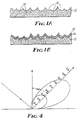
- the present invention provides a liquid crystal display device (Fig. 5) including a reflector assembly (Fig. 1B, Fig. 2B), said reflector assembly comprising one of the substrates of the device, this substrate having a micro-lenticular surface (Fig. 3A, Fig. 3B), a reflective structure overlying and substantially replicating the micro-lenticular surface, and a light transparent, low index outer organic layer overlying the reflective structure and also substantially replicating the micro-lenticular surface and in contact with liquid crystal material of the device which outer layer has an index of refraction not greater than 1.46 the index of refraction of Si0 2 .
- the invention provides a method for fabricating a reflective surface for liquid crystal display devices (Fig. 5) comprising:
- this invention is concerned with a method for preparing a liquid crystal display device which includes a new and improved reflector.
- the substrate for the reflector of the present invention preferably consists of a glass plate 12 which has a micro-lenticular surface on one major side of the glass plate.
- this micro-lenticular surface consists of concave shaped cavities or dimples having a depth ranging from about 0.5 to 2.5 pm and a diameter ranging from about 5 to 25 um.
- the generally concave shaped cavities 14, such as illustratively shown in Figure 1A will have a depth of from 1 to 2pm, and a diameter from 10 to 20pm.
- the surfaces to a certain extent resemble those obtained on metal and plastic surfaces by the peening action.
- a highly reflective layer 16 is deposited on the micro-lenticular surface of the substrate.
- the reflective layer for example, can consist of metals such as aluminum or silver.
- multi-layer dielectric films, such as Si0 2 and MgF 2 may also be used.
- the reflective layer is aluminum or silver, and most preferably is silver.
- a light transparent low index of refraction layer 18 is in optical contact with the reflective layer 16.
- the light transparent layer is composed of organic material and has an index of refraction not greater than that of Si0 2 .
- the reflective surface of the display device of the present invention can provide a reflection brightness three times greater than a diffuse surface up to 40° viewing angle.
- a reflector for a liquid crystal display device that resembles a 100 percent spreading surface with a well- controlled spreading lobe in optical contact with the liquid crystal material.
- the reflective layer deposited upon the micro-lenticular surface of the substrate of the present invention has a light reflecting profile which is substantially a spreading profile.
- the addition of a light transparent layer with a low index of refraction over and in optical contact with the reflective layer has the effect of widening the cone where total internal reflection will not occur, thus expanding the viewing angle over that obtainable with a diffuse reflector.
- the liquid crystal display devices of the present invention can achieve a 10:1 contrast ratio with greater than 55% brightness, compared with a 10:1 contrast with less than 40% brightness for similar displays with an external white reflector.
- the addition of the low index of refraction transparent overlayer is believed to cause light reflected from the micro-lenticular, reflectorized layer to be refracted back toward the direction of incident light. When the refracted light passes through the liquid crystal medium, it is incident on the top cover plate at a reduced angle.
- the refraction through the low index layer redirects some of the light, causing it to be incident on the top cover plate at less than the critical angle at that interface such that the light passes therethrough.
- the above described reflector is particularly suitable for the liquid crystal display devices disclosed in US Patent A-4 391,492.
- a preferred liquid crystal display device of the present invention utilizes a thermally addressable medium including cholesteric smectic liquid crystal compounds together with pleochroic dyes to provide an absorbing state, such devices being particularly useful in large scale, multiplexed applications.
- the thermally sensitive medium has a transition between at least two thermal phases, the lower being a smectic phase, and the upper being preferably a cholesteric phase.
- the medium develops two textures in the smectic phase: a light absorbing texture and a homeotropic texture.
- the homeotropic texture is developed in portions of the medium by sensitizing the medium as it passes rapidly from an upper thermal phase to the lower, smectic phase.
- the light absorbing texture is developed in the unsensitized portions of the medium as it goes through the transition to the smectic phase.
- the medium is sensitized by applying a voltage to those portions of the medium to be addressed.
- the addressed portions develop a substantially transparent light state, while the unaddressed portions develop a substantially light absorbing state.
- the coloring agent or dye which is locked within the liquid crystal medium as it develops its light absorbing texture in the smectic phase will absorb most of the light passing through the medium, the liquid crystal acting as a vehicle to orient the dye molecules into a light absorbing position.
- Electrodes disposed adjacent the medium are provided for sensitization. Heating electrodes are also provided to heat the medium to the upper thermal phase. In a multiplexed device, the electrodes define a matrix of columns and rows disposed substantially at right angles to each other, and in different planes.
- the row electrodes are made with a micro-lenticular substrate and overlying reflective and low index layers to provide high contrast as well as wide viewing angles. Such reflective electrodes further provide for a double pass of lightthrough the cell thus enhancing light absorption.
- the row electrodes are heated sequentially with electric current, and in x-y matrix operation, the display is written by applying voltages on the column electrodes. During the writing process, only the dots associated with the row where the heating current has just been removed are affected. In other words, only the dots where the liquid crystal material is rapidly cooling to the smectic state respond to the writing pulses on the column electrodes.
- the liquid crystal material cools rapidly through the nematic or cholesteric phase to the smectic phase, it can form two different textures.
- the liquid crystal material With a voltage applied on the column electrodes, the liquid crystal material is switched to a homeotropic state during the nematic or cholesteric phase and assumes the homeotropic smectic A texture after cooling is completed. Without the applied voltage, a light absorbing texture is developed instead.
- the dots associated with a rapidly cooling row electrode can be written into transparent state or a light absorbing state by applying or not applying voltages on the column electrodes.
- the smectic or cholesteric-smectic material used in such an embodiment preferably has positive dielectric anisotropy.
- Another preferred liquid crystal display device of the present invention utilizes the reflector structure as here disclosed in conjunction with a thermally activatable display device having a thermal barrier between the bottom, typically reflective electrodes, and a substrate which generally supports the liquid crystal medium, such as is disclosed in the above referenced US Patent 4 391 492.
- Such a construction may comprise an underlying substrate such as a glass plate onto which is applied a subassembly of a polymeric base having a micro-lenticular top surface with successive overlying reflective and low index layers.
- an underlying substrate such as a glass plate onto which is applied a subassembly of a polymeric base having a micro-lenticular top surface with successive overlying reflective and low index layers.
- the insulative character of the thermal barrier may be defined as a thermal layer having a coefficient of thermal conductivity approximately less than 62.8x10 -4 Js -1 cm -1 °C -1 (15x10 -4 cal sec -1 cm -1 °C -1 ).
- This thermal layer will allow the liquid crystal medium to absorb significantly more of the heat generated by the heating electrode.
- the thermal barrier or layer may have a cellular, voided or gas entrained structure to improve its insulative efficacy, although it will also function without this internal structure.
- This layer will generally include at least one organic polymer usually selected from a class of imides or amides. For this purpose, an imide quinoxaline polymer has been found to work well.
- vapor coated films of xylylene polymers such as poly(p-xylylene) and poly(chloro-p-xylylene) are desirably utilized, thus providing a very even and uniform coating which accurately conforms to the underlying substrate.
- the thermal barrier should be made with an approximate thickness in a range from 0.5 to 100 pm.
- a glass substrate which has at least one major surface having concave shaped cavities with depths in the range of about 0.5 to 2.5 ⁇ m and diameters ranging from about 5 to 25 um, and preferably depths of 1 to 2 11m and diameters of 10 to 20 ⁇ m.
- This micro-lenticular surface can be obtained by a combination of polishing and etching a glass plate. Indeed, it is particularly preferred to polish a soda-lime glass plate using a lapping machine, for example, such as a Highland Park Vi-Bro-Lap-model 20VL. In order to get effective polishing action, a thin layer of polishing mixture, such as a mixture of 30% by.
- the glass plate is then polished until a uniform diffuse surface is observed.
- the soda-lime glass can be polished from about 10-30 minutes to achieve such a surface.
- the glass is removed from the lapping machine and thoroughly cleaned.
- the so- polished glass has a very random rough surface. This surface roughness is reduced preferably by etching the glass in an appropriate etching solution, such as a 6:1 Buffered Oxide etch solution sold under the name of Buffor Oxide solution by Ashland Chemical Company, Specialty Chemical Division, Easton, Pennsylvania.
- the afor- mentioned Buffor Oxide solution generally it is preferably to etch the soda-lime glass for approximately 30 minutes to achieve the desired micro-lenticular surface properties. After etching, of course, the surface is cleaned with appropriate solvent or solvents, such as by treatment with deionized water, followed by rinsing with methanol.
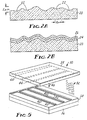
- the reduced roughness surface thus obtained is shown in cross-sectional view in Figure 2A, where, as determined with a surface topological probe, it may be seen that the surface of the glass substrate 20 mainly consists of shallow, less than 2 ⁇ m deep cavities 22 of roughly 10-20 ⁇ m diameter.
- the micro-structure of the resultant surface is further shown in the microphotographs of Figures 3A and 3B, which were prepared at 200x and 400x magnification respectively.
- a reflective layer 24 is deposited on the surface of the glass substrate 20.
- Any reflective material may be employed, such as aluminum, silver, metals and multi-film dielectric. However, in the practice of the present invention, it is particularly preferred to use aluminum or silver films.
- the reflective film can be deposited by well-known techniques. For example, aluminum or silver may be vacuum deposited on the micro-lenticular surface. The amount of metal deposited will, of course, depend on a variety of factors, such as the desired resistance of the device incorporating the reflective layer. In general, the light reflective layer will range in thickness from about 0.1 ⁇ m to about 1.5 um.
- a light transparent layer 26 is placed over and in optical contact with the reflective layer 24.
- the light transparent layer is one which has an index of refraction as low as possible.
- indices as high as that of thin-films of Si0 2 which are generally below about 1.46, and are preferably in the range from about 1.33 to 1.46, are preferred.
- the thickness of the low reflective index, transparent layer will be in the range of about 0.05 pm to 0.2 pm, and preferably about 0.1 um.
- the light transparent material can be deposited by any one of the known techniques, such as electron beam evaporation, and thermal vapor deposition.
- liquid crystal display devices having an internal reflector of the present invention exhibit significant improvement in brightness over similar displays employing an external white reflector.
- the device comprises a liquid crystal medium 32 containing a pleochroic dye, which medium is disposed between two glass substrate plates 34 and 36, respectively.
- the bottom substrate plate 36 has a micro-lenticular surface thereon.
- a thermal barrier 38 replicating the micro-lenticular surface is applied over the substrate 36, and a plurality of reflecting row electrodes 40, etc. are disposed over the barrier 38.
- films 42 of a low index material are deposited on top of the row electrodes, all of which replicate the micro-lenticular surface on the substrate 36.
- the row electrodes 40 make up one half of the x-y matrix for addressing the liquid crystal medium 32.
- the row electrodes 40 are made of electrically conductive, light reflective material such as silver or aluminum, deposited on the barrier 38.
- the top plate 34 supports a plurality of column electrodes 44, which make up the remaining half of the x-y matrix.
- the column electrodes 44 are electrically conductive and can be formed from materials such as indium oxide or tin oxide.
- the liquid crystal medium 32 is generally sealed such as by an epoxy preform (not shown) between the two substrate plates 34 and 36 with the electrodes on each side in optical contact with the liquid crystal medium.
- Light generally ambient
- the thermal barrier 38 insulates the row electrodes 40 and the liquid crystal medium 32 from the glass substrate 36 such that much of the heat generated by the row electrodes passes into the liquid crystal medium 32 and a smaller amount of the heat energy passes into substrate 36. This provides for a more efficient use of energy; the row electrodes now requiring less electrical current in order to cause a phase change in the liquid crystal medium.
- the micro-lenticular surfaced thermal barrier 38 is desirably formed of a material having a low thermal conductivity, i.e., less than 62.8x10- 4 J sec -1 cm -1 C -1 .
- a material having a low thermal conductivity i.e., less than 62.8x10- 4 J sec -1 cm -1 C -1 .
- a previously prepared micro-lenticular surface glass plate may be used as a master.
- the glass plate may be further processed, such as by electro-forming techniques, to provide a highly durable convex shaped master from which large quantities of approximately surfaced polymeric sheets may be replicated.
Landscapes
- Physics & Mathematics (AREA)
- General Physics & Mathematics (AREA)
- Optics & Photonics (AREA)
- Nonlinear Science (AREA)
- Mathematical Physics (AREA)
- Chemical & Material Sciences (AREA)
- Crystallography & Structural Chemistry (AREA)
- Liquid Crystal (AREA)
- Optical Elements Other Than Lenses (AREA)
- Devices For Indicating Variable Information By Combining Individual Elements (AREA)
Claims (18)
Applications Claiming Priority (2)
| Application Number | Priority Date | Filing Date | Title |
|---|---|---|---|
| US30899181A | 1981-10-06 | 1981-10-06 | |
| US308991 | 1981-10-06 |
Publications (3)
| Publication Number | Publication Date |
|---|---|
| EP0090855A1 EP0090855A1 (fr) | 1983-10-12 |
| EP0090855A4 EP0090855A4 (fr) | 1985-12-11 |
| EP0090855B1 true EP0090855B1 (fr) | 1989-07-12 |
Family
ID=23196202
Family Applications (1)
| Application Number | Title | Priority Date | Filing Date |
|---|---|---|---|
| EP19820903526 Expired EP0090855B1 (fr) | 1981-10-06 | 1982-10-05 | Affichage a cristaux liquides possedant un reflecteur a luminosite elevee |
Country Status (4)
| Country | Link |
|---|---|
| EP (1) | EP0090855B1 (fr) |
| JP (1) | JPS58501641A (fr) |
| DE (1) | DE3279816D1 (fr) |
| WO (1) | WO1983001310A1 (fr) |
Families Citing this family (4)
| Publication number | Priority date | Publication date | Assignee | Title |
|---|---|---|---|---|
| US4991940A (en) * | 1988-01-25 | 1991-02-12 | Taliq Corporation | Gain reflector-liquid crystal display |
| US5448069A (en) * | 1991-04-23 | 1995-09-05 | Buhler Ag Maschinenfabrik | Infrared measurement of constituents of particulate foodstuffs |
| GB9613802D0 (en) * | 1996-07-01 | 1996-09-04 | Nashua Corp | Improvements in or relating to light diffusers |
| GB2467374B (en) * | 2009-01-31 | 2011-08-10 | Devinder Roy Rattu | Mirror with enhanced reflection |
Family Cites Families (9)
| Publication number | Priority date | Publication date | Assignee | Title |
|---|---|---|---|---|
| US2601806A (en) * | 1948-09-30 | 1952-07-01 | Bausch & Lomb | Frustrated total reflection interference filter |
| US2911682A (en) * | 1955-02-28 | 1959-11-10 | Eastman Kodak Co | Method of casting a multireflector prism in a flexible mold |
| US3883214A (en) * | 1972-06-14 | 1975-05-13 | Westinghouse Electric Corp | Protective anti-reflective coatings for alkali-metal halide optical components |
| GB1434906A (en) * | 1972-08-04 | 1976-05-12 | Marconi Co Ltd | Liquid crystal display arrangements |
| US3938242A (en) * | 1973-09-27 | 1976-02-17 | Rca Corporation | Fabrication of liquid crystal devices |
| CH589306A5 (fr) * | 1975-06-27 | 1977-06-30 | Bbc Brown Boveri & Cie | |
| CH593533A5 (fr) * | 1975-11-26 | 1977-12-15 | Bbc Brown Boveri & Cie | |
| JPS5531588Y2 (fr) * | 1975-11-28 | 1980-07-28 | ||
| JPS5681887A (en) * | 1979-12-07 | 1981-07-04 | Seiko Instr & Electronics | Liquid crystal display unit |
-
1982
- 1982-10-05 EP EP19820903526 patent/EP0090855B1/fr not_active Expired
- 1982-10-05 DE DE8282903526T patent/DE3279816D1/de not_active Expired
- 1982-10-05 JP JP57503549A patent/JPS58501641A/ja active Pending
- 1982-10-05 WO PCT/US1982/001442 patent/WO1983001310A1/fr not_active Ceased
Also Published As
| Publication number | Publication date |
|---|---|
| EP0090855A1 (fr) | 1983-10-12 |
| DE3279816D1 (en) | 1989-08-17 |
| WO1983001310A1 (fr) | 1983-04-14 |
| JPS58501641A (ja) | 1983-09-29 |
| EP0090855A4 (fr) | 1985-12-11 |
Similar Documents
| Publication | Publication Date | Title |
|---|---|---|
| US4456336A (en) | High brightness internal reflector for liquid crystal displays and its method of fabrication | |
| US5513026A (en) | Method of producing a liquid crystal display with a spacer | |
| US7123324B2 (en) | Reflector providing particularly high reflectance in an intended viewing angle and reflection type liquid crystal display device using the same | |
| US4040727A (en) | Transflector | |
| US4252843A (en) | Process for forming a microstructured transmission and reflectance modifying coating | |
| JP2816285B2 (ja) | 透明ディスプレイ装置とその製造方法 | |
| US4519678A (en) | Liquid crystal display device | |
| CA1103499A (fr) | Traduction non-disponible | |
| US6861121B2 (en) | Optical diffusing layer, optical diffusing sheet, and optical element | |
| TWI290636B (en) | Optical member, method for producing the same, adhesive optical member and image viewing display | |
| US6421106B1 (en) | Reflector having pits and projections on a surface thereof, manufacturing method for the same, and reflection type liquid crystal display device employing the reflector | |
| US20030058547A1 (en) | Optical system | |
| EP0011644A4 (fr) | Dispositif à crystal liquide. | |
| GB2066545A (en) | Liquid crystal display device | |
| KR19990035897A (ko) | 반사판, 반사형 편광판 및 반사형 액정표시장치 | |
| KR960706687A (ko) | 영상표시 패널용 다층 반사 방지 코팅 | |
| KR20130095776A (ko) | 투명 도전성 소자, 입력 장치 및 표시 장치 | |
| JP3345089B2 (ja) | カラーフィルタ基板の作製方法 | |
| CN102804110A (zh) | 透明导电元件、输入装置以及显示装置 | |
| CN101356403A (zh) | 具有粘合层的光重定向膜 | |
| CN100383569C (zh) | 偏振光学元件及其制造方法和使用该元件的反射光学元件 | |
| TW200530654A (en) | Mechanical shutter | |
| EP0090855A1 (fr) | Affichage a cristaux liquides possedant un reflecteur a luminosite elevee. | |
| US20020118324A1 (en) | Substrate for a liquid crystal device, method of manufacturing a substrate for a liquid crystal device, a liquid crystal device, a method of manufacturing a liquid crystal device , and an electronic apparatus | |
| JP3748761B2 (ja) | 反射体および反射型液晶表示装置 |
Legal Events
| Date | Code | Title | Description |
|---|---|---|---|
| PUAI | Public reference made under article 153(3) epc to a published international application that has entered the european phase |
Free format text: ORIGINAL CODE: 0009012 |
|
| AK | Designated contracting states |
Designated state(s): CH DE FR GB LI NL |
|
| 17P | Request for examination filed |
Effective date: 19831004 |
|
| RBV | Designated contracting states (corrected) |
Designated state(s): CH DE FR GB LI NL |
|
| 17Q | First examination report despatched |
Effective date: 19870414 |
|
| GRAA | (expected) grant |
Free format text: ORIGINAL CODE: 0009210 |
|
| AK | Designated contracting states |
Kind code of ref document: B1 Designated state(s): CH DE FR GB LI NL |
|
| REF | Corresponds to: |
Ref document number: 3279816 Country of ref document: DE Date of ref document: 19890817 |
|
| ET | Fr: translation filed | ||
| PLBE | No opposition filed within time limit |
Free format text: ORIGINAL CODE: 0009261 |
|
| STAA | Information on the status of an ep patent application or granted ep patent |
Free format text: STATUS: NO OPPOSITION FILED WITHIN TIME LIMIT |
|
| 26N | No opposition filed | ||
| PGFP | Annual fee paid to national office [announced via postgrant information from national office to epo] |
Ref country code: FR Payment date: 19940916 Year of fee payment: 13 Ref country code: DE Payment date: 19940916 Year of fee payment: 13 Ref country code: CH Payment date: 19940916 Year of fee payment: 13 |
|
| PGFP | Annual fee paid to national office [announced via postgrant information from national office to epo] |
Ref country code: GB Payment date: 19940927 Year of fee payment: 13 |
|
| PGFP | Annual fee paid to national office [announced via postgrant information from national office to epo] |
Ref country code: NL Payment date: 19941031 Year of fee payment: 13 |
|
| PG25 | Lapsed in a contracting state [announced via postgrant information from national office to epo] |
Ref country code: GB Effective date: 19951005 |
|
| PG25 | Lapsed in a contracting state [announced via postgrant information from national office to epo] |
Ref country code: LI Effective date: 19951031 Ref country code: CH Effective date: 19951031 |
|
| PG25 | Lapsed in a contracting state [announced via postgrant information from national office to epo] |
Ref country code: NL Effective date: 19960501 |
|
| GBPC | Gb: european patent ceased through non-payment of renewal fee |
Effective date: 19951005 |
|
| REG | Reference to a national code |
Ref country code: CH Ref legal event code: PL |
|
| PG25 | Lapsed in a contracting state [announced via postgrant information from national office to epo] |
Ref country code: FR Effective date: 19960628 |
|
| PG25 | Lapsed in a contracting state [announced via postgrant information from national office to epo] |
Ref country code: DE Effective date: 19960702 |
|
| NLV4 | Nl: lapsed or anulled due to non-payment of the annual fee |
Effective date: 19960501 |
|
| REG | Reference to a national code |
Ref country code: FR Ref legal event code: ST |