EP0091304A1 - Verfahren und Anordnung für Gleichstrompolaritätswiederherstellung bei magnetischen Aufzeichnungen - Google Patents
Verfahren und Anordnung für Gleichstrompolaritätswiederherstellung bei magnetischen Aufzeichnungen Download PDFInfo
- Publication number
- EP0091304A1 EP0091304A1 EP83301880A EP83301880A EP0091304A1 EP 0091304 A1 EP0091304 A1 EP 0091304A1 EP 83301880 A EP83301880 A EP 83301880A EP 83301880 A EP83301880 A EP 83301880A EP 0091304 A1 EP0091304 A1 EP 0091304A1
- Authority
- EP
- European Patent Office
- Prior art keywords
- signal
- positive
- binary
- signals
- providing
- Prior art date
- Legal status (The legal status is an assumption and is not a legal conclusion. Google has not performed a legal analysis and makes no representation as to the accuracy of the status listed.)
- Granted
Links
Images


Classifications
-
- G—PHYSICS
- G11—INFORMATION STORAGE
- G11B—INFORMATION STORAGE BASED ON RELATIVE MOVEMENT BETWEEN RECORD CARRIER AND TRANSDUCER
- G11B20/00—Signal processing not specific to the method of recording or reproducing; Circuits therefor
- G11B20/10—Digital recording or reproducing
-
- G—PHYSICS
- G11—INFORMATION STORAGE
- G11B—INFORMATION STORAGE BASED ON RELATIVE MOVEMENT BETWEEN RECORD CARRIER AND TRANSDUCER
- G11B20/00—Signal processing not specific to the method of recording or reproducing; Circuits therefor
- G11B20/10—Digital recording or reproducing
- G11B20/10009—Improvement or modification of read or write signals
Definitions
- the present invention is concerned with a method and system for direct-current polarity restoration in magnetic recording.
- information When information is written onto a magnetic disc, the information is recorded in digital form.
- Digital square waves have vertical edges that a magnetic head can sense. Positive and negative transitions in the square wave, that is the edges, are recognized and recorded on the magnetic medium of the disc.
- the output When the magnetic head is used to read the data stored on the disc, the output is not in digital form because of the characteristics of the head and the magnetic medium.
- the signal read from the disc may include analog signals with flat regions between peaks. If the locations where the analog signal crosses the zero reference line can be determined, the outline of the original digital signal can be approximated.
- a zero-crossing detection device may be used to indicate when an applied signal crossed the base line.
- the signal transition edges could be detected and the original signal approximated.
- a flat region of the applied signal adjacent to the base line between peaks created an indeterminate output from the zero crossing detector. This flattening of the applied signal along the base line is called "shouldering".
- Prior solutions to this shouldering phenomenon included terminating the detection of zero crossings by binary gating during the period when the flat regions occurred between the peaks of the applied signals.
- a binary signal was used to operate the binary gate and if the binary signal was in error, the operation of the gate was also in error causing signel bit errors in the detector output.
- the binary gating generator typically had a long time delay associated with its electronics. Other electronic circuits within the equipment then required a matching time delay so that the desired output could be derived in timed sequence with the delayed binary signal.
- the present invention provides a system for restoring the direct-current component of a signal read from a storage medium, said system being characterized bv:
- the present invention further provides a method of restoring the direct-current component of a signal read from a storage medium, said method being characterized by the steps of:
- Polarity restoration entails shifting the shouldering region from the zero-axis or base line and restoring the zero-crossover points of the direct-current component of a signal read from a storage medium without the problems of time delay matching and single bit errors caused by binary gating.
- a transducer detects data recorded on a storage medium and produces isolated positive and negative analog signals which are converted to positive and negative binary signals by appropriate circuitry. These binary signals trigger an offset signal generator which provides either a positive or a negative offset signal depending upon the direction of the rate of change of the analog signal.
- the analog signals are also differentiated to form positive and negative differentiated analog signals which are summed with either the positive or the negative offset signal, respectively, to form a composite signal. Then the composite signal is differentially summed with the derivative of the analog signal of the opposite polarity to form a reconstructed signal which is applied to a zero-crossing detector.
- the detector output is a logical high-or-low-level signal which forms a binary square wave representative of the original data pattern.
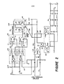
- FIG 1 is a block diagram of the elements of the direct-current polarity restoration apparatus according to the present invention.
- An original signal 10 recorded in a storage medium 50 is detected by a transducer 100 and is provided by a transducer-amplifier 110 in the form of isolated positive and negative analog signals 310, 311, as shown in Figure 4A.
- the signals 310 and 311 are introduced into the direct-current polarity resotration apparatus via a differentiator 120, provided by a differential amplifier, and a binary signal generator 130, simultaneously.
- the generator 130 senses a predetermined signal level and changes from one binary state to the other binary state when the signal 310 or 311 crosses that level, thus converting the signals 310, 311 to binary signals 320, 321, as shown in Figure 4B.
- the signals 320 and 321 are applied to an offset signal generator 140 which combats the problem of "shouldering" by providing either an offset signal 330 or 331, as shown in Figure 4C, to increase the level of the flat regions adjacent to the zero axis to well above or below the zero axis so that a zero-crossing detector 180 can distinguish a zero-axis crossing of a signal 190.
- the signal 330 or 331 is produced depends upon the slope of the analog signals 310, 311 at the appropriate time to eliminate the ambiguous shouldering regions adjacent to the zero axis.
- the signals 330, 331 are applied to a level shifter 150 which converts the signal with its amplitude shifted in proportion to the shift made by the generator 140. This results in level-shifted offset signals 350, 341, as shown in Figure 4E, that are next applied to a differential summer circuit 160.
- the signals 310 and 311 are also applied to the differentiator 120 which produces analog current signals 340 and 341, as shown in Figure 4D, that are derived from the applied voltage signals. Then the signals 340 and 350 or signals 34l and 35l are summed continuously within the differential summer circuit 160 to form a composite signal 360 or 361, as shown in Figure 4F. Then the signal 360 or 361 is differentially summed with the opposite polarity signal, either 340 or 341, resulting in a reconstructed signal 370, as shown in Figure 4G, which is reconverted into a voltage and then applied to the linear phase filter 170.
- the output of the filter 170 is applied to the zero-crossing detector circuit 180 which indicates the transitions in the signal 370 and provides a binary output signal 190 which can be processed by digital techniques.
- a transition of the signal 190 is equivalent to a transition of the original signal 10 recorded onto the storage medium 50.
- the transducer 100 senses the transitions in the storage medium 50, it converts the data into signals 310 and 311 which are amplified by the amplifier 110. These signals 310 and 311 are applied to the generator 130 which converts the signals 310, 311 to binary signals 320, 321 by sensing a predetermined non-zero level of signal amplitude and, when the signals 310 and 311 cross this level, amplifiers 131 and 132 conduct and trigger logic gates 133, 134, 135, and 136 to change the output signal level.
- the generator 130 toggles from a logical low to a logical high, and if signals 310 or 311 have a negative slope, then the generator 130 toggles from a logical high to a logical low.
- the signals 320 and 321 are applied to the generator 140 which supplies an offset signal, either 330 or 331, to increase the signal level within the shouldering regions of the signals 310 and 311 to permit the detector 180 to identify a zero axis crossing.
- the two signals 320 and 321 produced by the generator 130 can be used to initiate and terminate the signals 330 and 331.
- the signal 330 is generated from the signal 321 within the flat shouldering region after the signal 321 but before the signal 320, and the signal 331 is generated from the signal 320 in the flat shouldering region after the signal 320 but before the signal 321. Therefore, the signal 330 increases the level above the zero axis of the signals 310 and 311 having a positive slope within the shouldering region and the signal 331 increases the level below the zero axis of the signals 310 and 311 having a negative slope within the shouldering region. Since neither the signal 310 nor 311 can be positive and negative simultaneously, then only one offset signal 330 or 331 can be generated at any instant but both signals 330 and 331 are necessary to preserve the zero crossings.
- the signals 330 and 331 are applied to the level-shifter 150 which converts the signals 330 and 331 from a voltage to a current as a result of a potential difference across two resistors 151 and 152. Also, two transistors 153 and 154 shift the level of the signals 330 and 331 by a factor proportional to and controlled by the shift created by the generator 140 forming the signals 350 and 351 which are applied to the summer circuit 160.
- the signals 310 and 311 are also applied to the differential amplifier 120 which produces the signal 340 which is positive relative to ground reference and produces the signal 341 which is negative relative to ground reference.
- the signals 340 and 341, which are voltage signals are converted to current signals resulting from the potential difference across two resistors 121 and 122.
- the three current signals, namely, those generated by 340, 341, and 350 or 351 are simultaneously applied to the summer circuit 160.
- the signal 350 is available, it is summed with the signal 340 to provide the composite signal 360 which is then summed differentially with the signal 341 to provide the reconstructed signal 370.
- the signal 351 When the signal 351 is available, it is summed with the signal 341 to provide the composite signal 361 which is then summed differentially with the signal 340 to provide the reconstructed signal 370. Therefore, whether the signal 350 or 351 is available, only one reconstructed signal 370 is produced by the summer circuit 160 which is then applied to the filter 170 to eliminate distortion and noise before the signal 370 is applied to the detector 180.
- the detector 180 is a differential comparator that receives two signals, 181 and 182 from the filter 170, as shown in Figures 2 and 3. If these signals were summed, they would form the signal 370. Instead, these signals are differentially compared to form the output signal 190.
- the detector 180 When the signal 181 is greater than the signal 182, the detector 180 provides a fixed signal 190 greater than zero and when the signal 182 is greater than the signal 181, the detector 180 provides a fixed signal 190 less than zero.
- the binary signal at the output of the detector 180 has either a positive or negative level with every transition of the signal 181 or 182 forming a logical high and every non-transition forming a logical low.
- the present invention restores the direct current component of a signal read from a magnetic storage medium.
Landscapes
- Engineering & Computer Science (AREA)
- Signal Processing (AREA)
- Digital Magnetic Recording (AREA)
- Signal Processing For Digital Recording And Reproducing (AREA)
Applications Claiming Priority (2)
| Application Number | Priority Date | Filing Date | Title |
|---|---|---|---|
| US365661 | 1982-04-05 | ||
| US06/365,661 US4467374A (en) | 1982-04-05 | 1982-04-05 | Method and means for direct-current polarity restoration in magnetic recording |
Publications (2)
| Publication Number | Publication Date |
|---|---|
| EP0091304A1 true EP0091304A1 (de) | 1983-10-12 |
| EP0091304B1 EP0091304B1 (de) | 1986-06-18 |
Family
ID=23439801
Family Applications (1)
| Application Number | Title | Priority Date | Filing Date |
|---|---|---|---|
| EP83301880A Expired EP0091304B1 (de) | 1982-04-05 | 1983-03-31 | Verfahren und Anordnung für Gleichstrompolaritätswiederherstellung bei magnetischen Aufzeichnungen |
Country Status (4)
| Country | Link |
|---|---|
| US (1) | US4467374A (de) |
| EP (1) | EP0091304B1 (de) |
| JP (1) | JPS58185016A (de) |
| DE (1) | DE3364156D1 (de) |
Cited By (2)
| Publication number | Priority date | Publication date | Assignee | Title |
|---|---|---|---|---|
| EP0181784A1 (de) * | 1984-11-16 | 1986-05-21 | Sony Corporation | Erzeugungssystem für Digitalsignale und Verfahren dafür |
| DE19603858A1 (de) * | 1995-03-13 | 1996-09-19 | Fujitsu Ltd | Detektor für asymmetrische Signale und Signal-Regeneriervorrichtung, die denselben Detektor verwendet |
Families Citing this family (5)
| Publication number | Priority date | Publication date | Assignee | Title |
|---|---|---|---|---|
| US4686586A (en) * | 1986-01-21 | 1987-08-11 | Oki America, Inc. | Read back circuit for recovering data from magnetic storage medium |
| JPS6394411A (ja) * | 1986-10-07 | 1988-04-25 | Fuji Electric Co Ltd | デイスク記憶装置の読取信号再生回路 |
| JP2598733B2 (ja) * | 1992-03-06 | 1997-04-09 | ローム株式会社 | 磁気記録用書込み回路および磁気記録装置 |
| US5442492A (en) * | 1993-06-29 | 1995-08-15 | International Business Machines Corporation | Data recovery procedure using DC offset and gain control for timing loop compensation for partial-response data detection |
| US5420726A (en) * | 1994-02-17 | 1995-05-30 | Maxtor Corporation | Channel qualifier for a hard disk drive which differentiates a raw data signal before peak detection and qualification of the signal |
Citations (8)
| Publication number | Priority date | Publication date | Assignee | Title |
|---|---|---|---|---|
| US3617904A (en) * | 1969-06-05 | 1971-11-02 | Digitronics Corp | Noise insensitive peak detector |
| US3727143A (en) * | 1971-12-06 | 1973-04-10 | Ampex | Integrating level sensing circuit |
| US3898481A (en) * | 1974-03-28 | 1975-08-05 | Cincinnati Electronics Corp | Signal pulse detector |
| US3991376A (en) * | 1975-04-16 | 1976-11-09 | Randam Electronics, Inc. | Pulse height analyzer |
| US4016599A (en) * | 1976-03-19 | 1977-04-05 | Xerox Corporation | Anti-shouldering read circuit for magnetic disk memory |
| DE3025959A1 (de) * | 1979-07-10 | 1981-02-19 | Mfe Ltd | Verfahren und schaltungsanordnung zur dekodierung modifiziert-frequenzmodulierter signale |
| US4323932A (en) * | 1979-07-30 | 1982-04-06 | Sperry Corporation | Readback pulse compensator |
| US4342054A (en) * | 1979-06-06 | 1982-07-27 | Nakamichi Corporation | Information read device |
Family Cites Families (2)
| Publication number | Priority date | Publication date | Assignee | Title |
|---|---|---|---|---|
| US4371900A (en) * | 1981-01-23 | 1983-02-01 | Memorex Corporation | Equalization of DC null in reproducing a high density recording |
| US4346411A (en) * | 1981-02-17 | 1982-08-24 | International Business Machines Corporation | Amplitude sensitive three-level detector for derivative read back channel of magnetic storage device |
-
1982
- 1982-04-05 US US06/365,661 patent/US4467374A/en not_active Expired - Lifetime
-
1983
- 1983-03-31 EP EP83301880A patent/EP0091304B1/de not_active Expired
- 1983-03-31 DE DE8383301880T patent/DE3364156D1/de not_active Expired
- 1983-04-04 JP JP58059125A patent/JPS58185016A/ja active Granted
Patent Citations (9)
| Publication number | Priority date | Publication date | Assignee | Title |
|---|---|---|---|---|
| US3617904A (en) * | 1969-06-05 | 1971-11-02 | Digitronics Corp | Noise insensitive peak detector |
| US3727143A (en) * | 1971-12-06 | 1973-04-10 | Ampex | Integrating level sensing circuit |
| US3898481A (en) * | 1974-03-28 | 1975-08-05 | Cincinnati Electronics Corp | Signal pulse detector |
| US3991376A (en) * | 1975-04-16 | 1976-11-09 | Randam Electronics, Inc. | Pulse height analyzer |
| US4016599A (en) * | 1976-03-19 | 1977-04-05 | Xerox Corporation | Anti-shouldering read circuit for magnetic disk memory |
| DE2712037A1 (de) * | 1976-03-19 | 1977-09-22 | Xerox Corp | Leseschaltung fuer magnetplattenspeicher |
| US4342054A (en) * | 1979-06-06 | 1982-07-27 | Nakamichi Corporation | Information read device |
| DE3025959A1 (de) * | 1979-07-10 | 1981-02-19 | Mfe Ltd | Verfahren und schaltungsanordnung zur dekodierung modifiziert-frequenzmodulierter signale |
| US4323932A (en) * | 1979-07-30 | 1982-04-06 | Sperry Corporation | Readback pulse compensator |
Cited By (4)
| Publication number | Priority date | Publication date | Assignee | Title |
|---|---|---|---|---|
| EP0181784A1 (de) * | 1984-11-16 | 1986-05-21 | Sony Corporation | Erzeugungssystem für Digitalsignale und Verfahren dafür |
| DE19603858A1 (de) * | 1995-03-13 | 1996-09-19 | Fujitsu Ltd | Detektor für asymmetrische Signale und Signal-Regeneriervorrichtung, die denselben Detektor verwendet |
| US6052245A (en) * | 1995-03-13 | 2000-04-18 | Fujitsu Limited | Signal regenerating apparatus having asymmetrical signal detection circuit for detecting amplitude error and signal offset from a training signal and correcting same |
| DE19603858B4 (de) * | 1995-03-13 | 2005-03-24 | Fujitsu Ltd., Kawasaki | Signal-Regeneriervorrichtung |
Also Published As
| Publication number | Publication date |
|---|---|
| JPS58185016A (ja) | 1983-10-28 |
| DE3364156D1 (en) | 1986-07-24 |
| EP0091304B1 (de) | 1986-06-18 |
| JPH0376521B2 (de) | 1991-12-05 |
| US4467374A (en) | 1984-08-21 |
Similar Documents
| Publication | Publication Date | Title |
|---|---|---|
| US3668532A (en) | Peak detection system | |
| EP0284279B2 (de) | Stromkreis zum Nachweis von Impulsen unter Verwendung von Amplituden- und Zeitqualifikation | |
| US4590524A (en) | Multitrack PCM reproducing apparatus | |
| US4137504A (en) | Digital filter | |
| US4480276A (en) | Apparatus for peak detection in magnetic recording | |
| EP0091304B1 (de) | Verfahren und Anordnung für Gleichstrompolaritätswiederherstellung bei magnetischen Aufzeichnungen | |
| US4706236A (en) | Slice level corrector | |
| US3670249A (en) | Sampling decoder for delay modulation signals | |
| JPS5891514A (ja) | 信号変換回路 | |
| EP0430457B1 (de) | Verfahren und Gerät zur Qualifizierung der Datenpulse in einem durch einen magnetischen Kopf wiedergegebenen Signal der Datenfolge | |
| EP0158219A1 (de) | Auf Synchronisation ansprechender Taktgenerator für digitale Demodulatoren | |
| US4064408A (en) | Method and apparatus for detection of waveform peaks and slopes | |
| US4724496A (en) | Peak detector for magnetically recorded binary signal | |
| US20020015247A1 (en) | High resolution wide range write precompensation | |
| KR940000974B1 (ko) | 디지탈 신호 처리회로 | |
| US3496557A (en) | System for reproducing recorded digital data and recovering data proper and clock pulses | |
| EP0860827A2 (de) | Datenprüfung | |
| US4012785A (en) | Magnetic recording playback circuit | |
| EP0258671A2 (de) | Lese-Kanal-Architektur zur Verarbeitung von Lese-Kopf-Signalen | |
| JPS63153705A (ja) | 磁気記録装置の信号再生回路 | |
| US4152731A (en) | Read circuit for distinguishing false peaks in an alternating current playback signal | |
| KR930011378B1 (ko) | 3진데이타의 기록재생방법 | |
| KR880002694B1 (ko) | 신호 검출장치 | |
| JPH0469864A (ja) | 自動波形等化回路 | |
| JP2588907B2 (ja) | 信号検出装置 |
Legal Events
| Date | Code | Title | Description |
|---|---|---|---|
| PUAI | Public reference made under article 153(3) epc to a published international application that has entered the european phase |
Free format text: ORIGINAL CODE: 0009012 |
|
| 17P | Request for examination filed |
Effective date: 19830415 |
|
| AK | Designated contracting states |
Designated state(s): DE FR GB |
|
| RAP1 | Party data changed (applicant data changed or rights of an application transferred) |
Owner name: HEWLETT-PACKARD COMPANY |
|
| GRAA | (expected) grant |
Free format text: ORIGINAL CODE: 0009210 |
|
| AK | Designated contracting states |
Kind code of ref document: B1 Designated state(s): DE FR GB |
|
| REF | Corresponds to: |
Ref document number: 3364156 Country of ref document: DE Date of ref document: 19860724 |
|
| ET | Fr: translation filed | ||
| PLBE | No opposition filed within time limit |
Free format text: ORIGINAL CODE: 0009261 |
|
| STAA | Information on the status of an ep patent application or granted ep patent |
Free format text: STATUS: NO OPPOSITION FILED WITHIN TIME LIMIT |
|
| 26N | No opposition filed | ||
| PG25 | Lapsed in a contracting state [announced via postgrant information from national office to epo] |
Ref country code: GB Effective date: 19890331 |
|
| PG25 | Lapsed in a contracting state [announced via postgrant information from national office to epo] |
Ref country code: FR Free format text: LAPSE BECAUSE OF NON-PAYMENT OF DUE FEES Effective date: 19891130 |
|
| PG25 | Lapsed in a contracting state [announced via postgrant information from national office to epo] |
Ref country code: DE Effective date: 19891201 |
|
| GBPC | Gb: european patent ceased through non-payment of renewal fee | ||
| REG | Reference to a national code |
Ref country code: FR Ref legal event code: ST |