EP0091678A2 - Festkörper-Fernsehaufnahmeeinrichtung - Google Patents
Festkörper-Fernsehaufnahmeeinrichtung Download PDFInfo
- Publication number
- EP0091678A2 EP0091678A2 EP83103459A EP83103459A EP0091678A2 EP 0091678 A2 EP0091678 A2 EP 0091678A2 EP 83103459 A EP83103459 A EP 83103459A EP 83103459 A EP83103459 A EP 83103459A EP 0091678 A2 EP0091678 A2 EP 0091678A2
- Authority
- EP
- European Patent Office
- Prior art keywords
- shift register
- horizontal
- solid state
- state imaging
- imaging apparatus
- Prior art date
- Legal status (The legal status is an assumption and is not a legal conclusion. Google has not performed a legal analysis and makes no representation as to the accuracy of the status listed.)
- Withdrawn
Links
Images






Classifications
-
- H—ELECTRICITY
- H04—ELECTRIC COMMUNICATION TECHNIQUE
- H04N—PICTORIAL COMMUNICATION, e.g. TELEVISION
- H04N25/00—Circuitry of solid-state image sensors [SSIS]; Control thereof
- H04N25/70—SSIS architectures; Circuits associated therewith
- H04N25/76—Addressed sensors, e.g. MOS or CMOS sensors
Definitions
- the present invention relates to an improvement in solid state imaging apparatus having two-dimensionally disposed photodiodes with electronic switches for scanningly taking out outputs of the photosensitive elements.
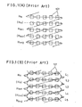
- the apparatus is designed to make the known interlace scannings. That is, as shown in FIG. 1(A), in a solid state apparatus having the two-dimensionally disposed phtosensitive elements 101, a scanning for a first field is made as shown by solid state horizontal lines. The scanning is made every two lines by skipping one lines inbetween, and in a second field, every two lines shown by dotted horizontal lines,which have not been scanned in the first field scanning, are scanned sequentially.
- two-line interlace scanning As one of modification of the above-mentioned interlace scanning method, there is a method which can be called two-line interlace scanning, such as disclosed in the Japanese published unexamined Patent Application Sho 51-56123.
- the above-mentioned two-line interlace scanning is elucidated referring to FIG. 1(B), wherein in the first field scanning, adjacent picture elements of two lines L 1 and L 2 , and subsequently L 3 and L 4 , and subsequently L 5 and L 6 are simultaneously scanned as shown by solid horizontal lines. And in the second field scanning, scanning is made shifting by one line, that is horizontal lines L 2 and L 3 are simultaneously scanned, and subsequently the horizontal lines L 4 and L 5 are simultaneously scanned.
- Such two-line interlace scanning has advantage in improved after image characteristic. The reason of the advantage is elucidated as follows.
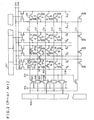
- selection gate 209 for each photodiode 210 as picture element is connected to receive control signal from horizontal read out signal line 217, and to give output signal to vertical line 218.
- the solid horizontal lines indicate horizontal scannings in the first field and the dotted horizontal lines indicate horizontal scannings in the second field
- H n , H n+1' H n+2 ... indicate nth, (n+l)th, (n+2)th ... lines of the first field, respectively
- (H n ), (H n+1 )' (H n+2 ) ... indicate nth, (n+l)th, (n+2)th ... lines of the second field, respectively.
- the horizontal control signal line 217 consisting of n lines, L 1' L 2' L 3 ... L are made conductive at positive potential of the horizontal lines.
- Second selection gate 203 and 204 are for "switching among the vertical lines 218 consisting of l 1 , l 2' l 3 ... l m ' so as to control signals on the vertical lines to output terminals 215 and 216.
- the second selection gate 203 and 204 are selectively switched on by signals from horizontal shift register 201, which is for selective switching on of the second selection gates 203 and 204 for a horizontal scanning, to produce horizontally scanned output signal to the output terminals 215 and 216.
- the output terminals 215 and 216 are sequentially connected to selected vertical read-out signal lines l 1 and l 2 , or l 3 and l 4 ,or l 5 and k 6 ....
- field signal pulse is impressed on either terminal 213 or 214 depending on the first field or the second field, respectively. Accordingly, in the first field the line selection gates 205 and 206 are switched on by the field signal impressed on the field signal terminal 213, and in the second field the line selection gates 207 and 208 are switched on by field signal impressed on the field signal terminal 214.
- the vertical control signal pulses are issued from the vertical shift register 202 to the pair of lines l 1 and l 2 , the pair of lines l 3 and l 4 , ...., and in the second field to the pair of lines l 2 and l 3 , the pair of lines l 4 and l 5 ,....
- photoelectric signals of the photoelectric element is issued through the first selection gates209 and 211, and through the second selection gates 203 and 204 to the output terminals 215 and 216, respectively, thereby to make the two-line scanning as shown in FIG. l(B).
- the above-mentioned prior art example apparatus has a shortcoming of producing flicker depending on the condition of driving (as disclosed in an article: Television Gakkai (Academy) 1981 National Conference Report, p. 63, Ando et al.) Outline of the shortcomina is elucidated hereafter.
- the photodiodes 210, 212 ... have stray capacities C 1' and C'with the horizontal read-out signal lines 217.
- the control signal from the vertical shift resister 202 is impressed in the first field to the pair of L 1 + L 2 , L 3 + L 4 ,... , and in the second field to the pair of L 2 + L 3 , L 4 + L 5 ...., respectively.
- respective photodiodes under the read-out condition are in the following states.
- the photodiode 210 is impressed with control signals of the horizontal lines L 1 and L 2 through the stray capacities C'and C 2'
- the photodiode 210 is impressed with the control signal of the horizontal line L 2 only, since in the second line the horizontal line L 1 has no vertical control signal.
- the photodiode 212 is impressed with, in the first field,the control signal of the horizontal line L 2 only, and in the second field, with both the control signal of the horizontal lines L2 and L 3' That is, in the first field and in the second field, the photodiodes 210 and 212 receive different voltages originated by the control signals on the horizontal lines to the stray capacities. And this difference of the control pulses given on the photodiodes causes undesirable fractuation of output signals field by field, that is,a flickering of picture produced.
- one measure to be considered may be to minimize the undesirable stray capacities.
- the solid state imaging apparatus have a large number of photodiodes on a very small wafer together with a number of wiring lines, it is almost impossible to substantially eliminate the stray capacities.
- the present invention proposes a novel improved configuration of the solid state imaging apparatus wherein the above-mentioned shortcomings of the prior art can be eliminated.
- horizontal read-out lines L 1 , L2 , L 3 ... L are connected directly to respective output terminals of a vertical shift register 302, and within one horizontal scanning type period, at least two vertical control pulses are issued at differrent time points from each other to neighboring two stages of the vertical shift register 302 so as to read-out photoelectric signals of each other neighboring lines therewith.
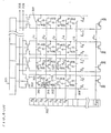
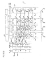
- FIG. 3 A preferred example of solid state imaging apparatus embodying the present invention is shown in FIG. 3 and a vertical shift register 302 of the circuit of FIG. 3 is shown FIG. 4.
- the line selection gates connected between the horizontal lines L 1' L 2 ... L n and the output terminals of the vertical shift register are omitted in the embodiment circuit of FIG. 3, and the vetical shift register 302 has the same number of stages as that of the horizontal lines L 1 ... L n .
- the vertical shift register 302 is known circuit as such and is constituted as shown in FIG. 4. Principle of operation of the circuit of FIG. 4 is elucidated with reference to waveforms of FIG. 5 wherein a pair of clock signal 0 ⁇ 1 and 0 ⁇ 2 are impressed on the input terminsls 0 ⁇ 1 - and 0 ⁇ 2 of FIG. 4, respectively.
- a starting pulse 0 ⁇ ST shown in FIG. 5 is impressed to a starting pulse input terminal 0 ⁇ ST of FIG. 4.
- the output terminals O 1 , 0 2 , O 3 ... correspond to the output terminals O 1 , 0 2 , 03 ... of the vertical shift register 302 of FIG. 3, respectively.
- FIG. 5 Principle of operation of the circuit of FIG. 4 is elucidated with reference to waveforms of FIG. 5 wherein a pair of clock signal 0 ⁇ 1 and 0 ⁇ 2 are impressed on the input terminsls 0 ⁇ 1 - and 0 ⁇ 2 of FIG. 4, respectively.
- the second clock signal 0 ⁇ 2 turns to H potential
- the first clock signal turns to L potential
- the MOS FET 400, 402 and 403 turn to cut-off state, and therefore the MOS FET 401 is kept in ON state by means of voltage across the capacitance C 1 .
- a MOS FET 404 is ON, and at this time point of t 1 , the output terminal O 1 turns to H potential by connection through the MOS FET 401 to the second clock pulse terminal ⁇ 2 .
- the capacitance C 2 is charged to make a point N 2 as a result of charging through the ON-state transistor 404 and 401.
- the MOS FET 400 turns on as a result of H state of the first clock signal ⁇ 1 , and being at L potentials of the starting signal ⁇ ST and the second clock signal ⁇ 2 , the charge of the capacitor C l is discharged through the MOS FET 400. Accordingly, the MOS FET 401 is cut off, thereby the output terminal O 1 is kept at L potential.
- the MO S FET 405 turns on by means of the charged voltage across the capacitance C 2 , making the MOS FET 406 and 407 cut off. Accordingly, the output terminal 0 2 becomes to H potential by connection through the MOS FET 405 to the first clock signal terminal ⁇ 1 .
- the MOS FET 408 turns on as the clock signal becomes H , and a capacitance C 3 is charged, thereby making a point N 3 to H potential.
- the output terminal 0 2 upon becoming L of the first clock signal ⁇ 1 , the output terminal 0 2 becomes L, but at this time the voltage across the capacitance C 3 is kept since the MOS FET 408 is cut off.
- the MOS FET 409 is ON and the capacitance C 3 is charged, and the MOS FET 410 and 411 are cut off. Accordingly, the output terminal O 1 is H since it is connected to the second clock signal terminal ⁇ 2 through the MOS FET 409.
- the MOS FET 403 is ON, and the MOS FET 404 turns ON since second clock signal terminal ⁇ 2 is H.
- first signal clock ⁇ 1 is L and MOS FET 404 and 403 are ON, and charge in the capacitance C 2 is discharged through the MOS FET 403 and 404, thereby cutting off the MOS FET 405.
- H potential of the output terminal 0 3 charges the capacitor C 4 through MOS FET 412 which is switched on by H potential of the clock signal ⁇ 2 .
- pulse potential input to the input terminal ⁇ ST in turn makes the output terminals O 1 , 0 2 , 03 .. to H potential responding to incoming of the pulses of clock signals ⁇ 1 and ⁇ 2 .
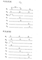
- pulse train of output signals at output terminals O 1 , O 2 , O 3 , O 4 ... is obtainable as shown in FIG. 6(A) and FIG. 6(B). That is,in the first field shown in FIG.
- input signal ⁇ ST fed into the vertical shift register 302 at the time point of the pulse of the first clock signal ⁇ 1 is output to the first output terminal O 1 at the time point of the pulse of the second clock signal ⁇ 2 after one horizontal scanning time period H, and to the output terminal 0 2 the pulse is issued at the time point of a pulse in the second clock signal ⁇ 2 immediately after the above-mentioned output to the first output terminal O 1 .
- the output terminals 0 3 and O 4 the above-mentioned steps at the output terminals O 1 and 0 2 repeat in the same way. Accordingly, the output signals are issued,making signal pairs of pair O 1 and O 2 , pair 0 3 and O 4 , ... repeating at every time period of one horizontal scanning.
- input signal ⁇ ST fed into the vertical shift register 302 at the time point of the pulse of the first clock signal ⁇ 1 , is output to the first output terminal O 1 at the time point of the pulse of the second clock signal after one horizontal scanning time period H, and to the output terminal 0 2 the pulse is issued at the time point of a pulse in the second clock signal ⁇ 2 immediately after the above-mentioned output to the first output terminal O 1 .
- the output terminals 0 4 and 0 5 the above-mentioned steps at the output terminals 0 2 and 0 3 repeat in the same way. Accordingly, the output signals are issued making such signal pairs as pair 0 2 and 0 3' pair 0 4 and 0 5 , ...,repeating at every time period of one horizontal scanning.
- Objective image projected on the photodiodes 305 is converted into electric signal by the photodiode 305, and the electric signal is read out through a first selection gate 315 controlled by control signal even through a first horizontal line 307 (L1), and through a vertical line 306 (l 1 ) and further through a second selection gate 303 to a first output terminal 308.
- Output signal from the photodiode 305' of the second line is similarly read out through another first selection gate 316, through another vertical line l 2 and further through another second selection gate 304 to a second output terminal 309.
- the second selection gates 303 and 304 are controlled by a horizontal shift register 301, thereby horizontally scanning the output signal in the horizontal direction.
- the vertical shift register 302 is driven in the manner as elucidated with reference to FIG. 6(A) and FIG. 6(B). Accordingly, as has been elucidated with reference to FIG. 4 and FIG. 6(A) and FIG. 6(B), the control signal impressed on the horizontal , lines 307 are impressed on a pair of L 1 and L 2 , a next pair of L 3 and L 4 , further next pair of L 5 and L 6 ... in the first field. And in the second field, control pulses are impressed on a pair of L 2 and L 3 , another pair of L 4 and L 5 , .... Thus the above-mentioned simultaneous two-line vertical scanning is made.
- the horizontal lines receive vertical control signals O 1 , O 2 , O 3 , O 4 , ... of FIG. 6 (A) or FIG. 6 (B). That is in a manner that the control signal pairs O 1 and O 2 , or 0 3 and O 4 , ... of FIG. 6 (A), or 0 2 and O 3 , or 0 4 and O 5 , ... in FIG. 6(B) are given with small time differences between the pulses within each pair as shown in FIG. 6(A) and FIG. 6(B).
- the starting signal ⁇ ST has covered . timing of both pulses of each pair of the clock signals ⁇ 1 and ⁇ 2 , but apart from the above example, it is only necessary that the starting signal ⁇ ST should be in synchronism merely to the first clock signal ⁇ 1 And the first pulse of the second clock signal ⁇ 2 , which is within a timing covered by the duty time of the signal pulse of the starting signal ⁇ ST , is not necessarily required.
- the embodiment of FIG. 3 has no shortcoming of the flickering and furthermore, switching devices which has been necessitated between the output terminals of the vertical shift-register and the horizontal lines can be eliminated.
- the read out signals of a photodiode 305 and a next photodiode 305' are given to the output terminals 308 and 309 through the first selection switches 315 and 316, and second selection switches 303 and 304, respectively, by controlling of a corresponding stage of the horizontal shift register 301.
- the two read out signals at the output terminals 308 and 309 which are read out by two pulses in the same pair, such as O 1 and O 2 , or 0 3 and 0 4 in FIG . 6 (A), or O 2 and O 3 , or 0 4 and 0 5 in FIG. 6(B), are always summed up by a circuit (not shown in FIG. 3) to produce one signal of a picture element of one horizontal line of the two-line scanning.
- Clock signals ⁇ 1 and ⁇ 2 of FIG. 6(A) and FIG. 6(B) can be produced, for instance, by using a circuit shown in F IG . 7 wherein double phase driving pulses ⁇ a and ⁇ b are interchangedly issued by means of control signal ⁇ F (H, L).
- the output connection of the shift register 302' is made between even number output terminals and sequential horizontal lines, that is, output terminals 0 2 , O 4 , 0 6 ... are connected to the horizontal lines L 1 , L 2 , L 3 ...
- the first clock signal ⁇ 1 and the second clock signal ⁇ 2 each has two pulses within every horizontal scanning period time, thereby shifting the shift register 302' for two-steps in each horizontal scanning time, thereby sending two-paired pulses O 1 and O 3 , or 0 5 and O 7 , or 0 3 and O 5 , or 0 7 and O 9 ... to paired neighboring two horizontal lines.
- the switching for the fields is made by shifting the phase of the ⁇ ST pulses with respect to the clock signals ⁇ 1 and ⁇ 2 , as shown in FIG. 8(A) and FIG. 8(B).
- pair pulses O 1 and 0 3 , or O 5 and O 7 ... as in FIG. 8(A) or the pair pulses 0 3 and O 5 , or 0 7 and 0 9 ... as in FIG. 8(B) are obtainable.
- the duty time of the pulse ⁇ ST may be such that it covers only the pulse of the first clock signal ⁇ 1 , and it is sufficient that the duty time of the pulse ⁇ ST covers only the timing of a pulse of the first clock signal ⁇ 1 .
- FIG. 9 shows a modired example of the clock signals wherein clock signal ⁇ 2 is only an inversed signal to the clock signal of ⁇ 1 .
- the clock signal generator can be simplified.
- connection between the shift register output terminals and the horizontal lines can be made with a buffer circuit inbetween as shown in FIG. 10 or FIG. ll.
- the buffer circuit 2000 has source-to- drain series-connected MOS FET 1001 + 1002, 1001' + 1002' ... and gate of the first MOS FETs 1001, 1001' ... are connected to the output terminal O 1 0 2 .. of the shift register 302, and gates of the other MOS FETs 1002, 1002' ... are common connected to the clock signal input terminal ( ⁇ 1 + ⁇ 2 ). And sources of the MOS FET 1001, 1001' ... are connected to positive power source terminal. And junction points O 1 ' 0 2 ' ... between the source-drain series-connection are connected to the horizontal lines L 1 , L 2 .... This circuit can provide the same control signals as the preceding examples and further enables to adjust DC mean potential of the horizontal lines.
- FIG. 11 shows still another modification which has another buffer circuit 2001 between the shift register and the horizontal lines.
- the buffer circuit comprises a set of latches . 1105, 1105', acrossEach latch 1105 ... comprises MOS FET 1101, 1102, 1103 and capacitor 1104, wherein a pair of clock signals ⁇ 3 and ⁇ 3 which is inverse to ⁇ 3 , are impressed, and thereby the output pulses of the shift register 302' are latched.
- the transistors 1101, 1102 and 1103 perform similar functions as those of transistors 400, 401, 401, 402 and C 1 of F I G. 4.
- Each of the circuits 1105, 1105', 1105" ...
- the pulse ⁇ 3 should cover the timing of the inverse signal of the logic sum of the signals ⁇ 1 and ⁇ 2 . For instance, if clock signal pulses ⁇ 1 , ⁇ 2 and ⁇ 3 as shown in FIG. 11 are used, then output pulses of the additional shift registers 1105 + 1005' + 1005" + ... are issued in synchronism with the clock signal ⁇ 3 . Accordingly, the horizontal lines can receive the control signals in the same way as that of the preceding examples.
- FIG. 10 and fig. 11 the brightness fractuation problems have been overcome.
- number of stage of the vertical shift register 302 become twice as large as the number of the vertical shift register of FIG. 2.
- the number of stages of the vertical shift registers are the same as that of FIG. 2, accordingly the circuit configuration and cost is moderate.
- the circuit is advantageous with regard to driving pulse voltage. That is, in the circuit of FIG. 10, in order to turn on MOS FET, for instance 1001, it is necessary to provide a driving pulse which is higher by threshold voltage of the MOS FET above that of the output terminal 0 1 of the shift register.
- bootstrap circuit is constituted by a capacitor 1104, therefore the voltage of the MOS FET 1102 easily turns on the MOS FET 1102 if the output potential of the shift register O 1 is higher than the threshold value.
Landscapes
- Engineering & Computer Science (AREA)
- Multimedia (AREA)
- Signal Processing (AREA)
- Transforming Light Signals Into Electric Signals (AREA)
Applications Claiming Priority (4)
| Application Number | Priority Date | Filing Date | Title |
|---|---|---|---|
| JP61472/82 | 1982-04-12 | ||
| JP57061472A JPS58178674A (ja) | 1982-04-12 | 1982-04-12 | 固体撮像装置 |
| JP58054366A JPS59181780A (ja) | 1983-03-30 | 1983-03-30 | 固体撮像装置 |
| JP54366/83 | 1983-03-30 |
Publications (2)
| Publication Number | Publication Date |
|---|---|
| EP0091678A2 true EP0091678A2 (de) | 1983-10-19 |
| EP0091678A3 EP0091678A3 (de) | 1984-11-28 |
Family
ID=26395122
Family Applications (1)
| Application Number | Title | Priority Date | Filing Date |
|---|---|---|---|
| EP83103459A Withdrawn EP0091678A3 (de) | 1982-04-12 | 1983-04-08 | Festkörper-Fernsehaufnahmeeinrichtung |
Country Status (2)
| Country | Link |
|---|---|
| EP (1) | EP0091678A3 (de) |
| CA (1) | CA1204502A (de) |
Cited By (1)
| Publication number | Priority date | Publication date | Assignee | Title |
|---|---|---|---|---|
| EP0851497A3 (de) * | 1996-12-24 | 2000-05-17 | Mitsubishi Denki Kabushiki Kaisha | Focalebenenmatrix und Ansteuerungsverfahren davon |
Family Cites Families (2)
| Publication number | Priority date | Publication date | Assignee | Title |
|---|---|---|---|---|
| JPS585627B2 (ja) * | 1977-08-10 | 1983-02-01 | 株式会社日立製作所 | 固体撮像装置 |
| FR2534435B1 (fr) * | 1982-10-08 | 1986-05-09 | Thomson Csf | Camera de television couleur monosenseur |
-
1983
- 1983-04-08 EP EP83103459A patent/EP0091678A3/de not_active Withdrawn
- 1983-04-11 CA CA000425619A patent/CA1204502A/en not_active Expired
Cited By (1)
| Publication number | Priority date | Publication date | Assignee | Title |
|---|---|---|---|---|
| EP0851497A3 (de) * | 1996-12-24 | 2000-05-17 | Mitsubishi Denki Kabushiki Kaisha | Focalebenenmatrix und Ansteuerungsverfahren davon |
Also Published As
| Publication number | Publication date |
|---|---|
| EP0091678A3 (de) | 1984-11-28 |
| CA1204502A (en) | 1986-05-13 |
Similar Documents
| Publication | Publication Date | Title |
|---|---|---|
| US4805026A (en) | Method for driving a CCD area image sensor in a non-interlace scanning and a structure of the CCD area image sensor for driving in the same method | |
| US4959723A (en) | Solid state image pickup apparatus having multi-phase scanning pulse to read out accumulated signal | |
| KR920003654B1 (ko) | 고속셔터 기능이 있는 고체 촬상소자 | |
| EP0403248B1 (de) | Photoelektrisches Umwandlungsgerät | |
| US3995107A (en) | Charge coupled parallel-to-serial converter for scene scanning and display | |
| US4531156A (en) | Solid state image pickup device | |
| US4117510A (en) | Solid state color imaging apparatus | |
| EP0039177A2 (de) | Festkörper-Bildaufnahmeeinrichtung | |
| US6496224B2 (en) | Imaging device including thinned read out mode and all pixel read out mode | |
| US4212034A (en) | Solid-state image pickup device | |
| GB2151878A (en) | Charged coupled device imagers with partitioned registers | |
| US5539536A (en) | Linear imaging sensor having improved charged transfer circuitry | |
| US4626916A (en) | Solid state image pickup device | |
| US4761689A (en) | Apparatus for driving a solid state image pickup device | |
| JP2736121B2 (ja) | 電荷転送装置及び固体撮像装置 | |
| US4578707A (en) | Method of reducing vertical smears of a solid state image sensor | |
| US5796432A (en) | Method of and apparatus for solid state imaging device | |
| AU607724B2 (en) | Charge-coupled device | |
| US5379068A (en) | Solid state imaging devices for producing normal and mirror image signals with the use of a reversible shift register | |
| US4851917A (en) | Solid state image pickup apparatus with interlaced row pair readout | |
| JPS6387874A (ja) | 固体撮像装置 | |
| US4866528A (en) | Image pickup apparatus providing lessened flicker in electronic still cameras and the like | |
| EP0091678A2 (de) | Festkörper-Fernsehaufnahmeeinrichtung | |
| US5998778A (en) | Focal plane array and driving method therefor | |
| KR100305334B1 (ko) | 클럭신호위상이스위칭되는촬상장치의신호전하전송방법 |
Legal Events
| Date | Code | Title | Description |
|---|---|---|---|
| PUAI | Public reference made under article 153(3) epc to a published international application that has entered the european phase |
Free format text: ORIGINAL CODE: 0009012 |
|
| AK | Designated contracting states |
Designated state(s): DE FR GB |
|
| PUAL | Search report despatched |
Free format text: ORIGINAL CODE: 0009013 |
|
| AK | Designated contracting states |
Designated state(s): DE FR GB |
|
| 17P | Request for examination filed |
Effective date: 19850202 |
|
| STAA | Information on the status of an ep patent application or granted ep patent |
Free format text: STATUS: THE APPLICATION HAS BEEN WITHDRAWN |
|
| 18W | Application withdrawn |
Withdrawal date: 19860507 |
|
| RIN1 | Information on inventor provided before grant (corrected) |
Inventor name: FUJIMOTO, MAKOTO |