EP0091739A1 - Tête magnétique de lecture intégrée, magnétostrictive-piézoélectrique MOS - Google Patents
Tête magnétique de lecture intégrée, magnétostrictive-piézoélectrique MOS Download PDFInfo
- Publication number
- EP0091739A1 EP0091739A1 EP83301491A EP83301491A EP0091739A1 EP 0091739 A1 EP0091739 A1 EP 0091739A1 EP 83301491 A EP83301491 A EP 83301491A EP 83301491 A EP83301491 A EP 83301491A EP 0091739 A1 EP0091739 A1 EP 0091739A1
- Authority
- EP
- European Patent Office
- Prior art keywords
- film
- thin
- magnetostrictive
- piezoelectric
- substrate
- Prior art date
- Legal status (The legal status is an assumption and is not a legal conclusion. Google has not performed a legal analysis and makes no representation as to the accuracy of the status listed.)
- Granted
Links
- 239000004065 semiconductor Substances 0.000 title description 3
- 229910044991 metal oxide Inorganic materials 0.000 title description 2
- 150000004706 metal oxides Chemical class 0.000 title description 2
- 239000010408 film Substances 0.000 claims abstract description 127
- 239000010409 thin film Substances 0.000 claims abstract description 114
- 239000000758 substrate Substances 0.000 claims abstract description 59
- 239000000463 material Substances 0.000 claims abstract description 26
- 239000007787 solid Substances 0.000 claims abstract description 9
- 230000010287 polarization Effects 0.000 claims abstract description 5
- 230000035699 permeability Effects 0.000 claims description 10
- 239000004020 conductor Substances 0.000 claims description 9
- 230000008878 coupling Effects 0.000 claims description 9
- 238000010168 coupling process Methods 0.000 claims description 9
- 238000005859 coupling reaction Methods 0.000 claims description 9
- 230000001939 inductive effect Effects 0.000 claims description 9
- 238000004804 winding Methods 0.000 claims description 7
- 230000008859 change Effects 0.000 claims description 4
- XLOMVQKBTHCTTD-UHFFFAOYSA-N Zinc monoxide Chemical compound [Zn]=O XLOMVQKBTHCTTD-UHFFFAOYSA-N 0.000 description 21
- 229910052710 silicon Inorganic materials 0.000 description 15
- XUIMIQQOPSSXEZ-UHFFFAOYSA-N Silicon Chemical compound [Si] XUIMIQQOPSSXEZ-UHFFFAOYSA-N 0.000 description 14
- 239000010703 silicon Substances 0.000 description 14
- 239000002033 PVDF binder Substances 0.000 description 12
- PXHVJJICTQNCMI-UHFFFAOYSA-N Nickel Chemical compound [Ni] PXHVJJICTQNCMI-UHFFFAOYSA-N 0.000 description 10
- 239000011787 zinc oxide Substances 0.000 description 10
- 238000000151 deposition Methods 0.000 description 9
- 229910052782 aluminium Inorganic materials 0.000 description 7
- XAGFODPZIPBFFR-UHFFFAOYSA-N aluminium Chemical compound [Al] XAGFODPZIPBFFR-UHFFFAOYSA-N 0.000 description 7
- 230000008021 deposition Effects 0.000 description 7
- 239000003990 capacitor Substances 0.000 description 6
- 230000004907 flux Effects 0.000 description 6
- PCHJSUWPFVWCPO-UHFFFAOYSA-N gold Chemical compound [Au] PCHJSUWPFVWCPO-UHFFFAOYSA-N 0.000 description 6
- 229910052737 gold Inorganic materials 0.000 description 6
- 239000010931 gold Substances 0.000 description 6
- 229910005347 FeSi Inorganic materials 0.000 description 5
- 238000000034 method Methods 0.000 description 5
- 238000010276 construction Methods 0.000 description 4
- 229910052759 nickel Inorganic materials 0.000 description 4
- 229920003229 poly(methyl methacrylate) Polymers 0.000 description 4
- 239000004926 polymethyl methacrylate Substances 0.000 description 4
- 239000004593 Epoxy Substances 0.000 description 3
- 239000000853 adhesive Substances 0.000 description 3
- 230000001070 adhesive effect Effects 0.000 description 3
- 238000004519 manufacturing process Methods 0.000 description 3
- 229910052751 metal Inorganic materials 0.000 description 3
- 239000002184 metal Substances 0.000 description 3
- 239000000203 mixture Substances 0.000 description 3
- 125000006850 spacer group Chemical group 0.000 description 3
- IJGRMHOSHXDMSA-UHFFFAOYSA-N Atomic nitrogen Chemical compound N#N IJGRMHOSHXDMSA-UHFFFAOYSA-N 0.000 description 2
- 238000000137 annealing Methods 0.000 description 2
- 239000000919 ceramic Substances 0.000 description 2
- 230000003247 decreasing effect Effects 0.000 description 2
- 230000005684 electric field Effects 0.000 description 2
- 230000006870 function Effects 0.000 description 2
- 238000011065 in-situ storage Methods 0.000 description 2
- 238000010884 ion-beam technique Methods 0.000 description 2
- 238000002955 isolation Methods 0.000 description 2
- 229910002555 FeNi Inorganic materials 0.000 description 1
- 229910000676 Si alloy Inorganic materials 0.000 description 1
- BQCADISMDOOEFD-UHFFFAOYSA-N Silver Chemical compound [Ag] BQCADISMDOOEFD-UHFFFAOYSA-N 0.000 description 1
- 230000009471 action Effects 0.000 description 1
- 230000003321 amplification Effects 0.000 description 1
- 239000000969 carrier Substances 0.000 description 1
- 238000001514 detection method Methods 0.000 description 1
- 230000000694 effects Effects 0.000 description 1
- 238000005516 engineering process Methods 0.000 description 1
- 238000007667 floating Methods 0.000 description 1
- 239000011521 glass Substances 0.000 description 1
- 238000010438 heat treatment Methods 0.000 description 1
- 239000012212 insulator Substances 0.000 description 1
- 238000007737 ion beam deposition Methods 0.000 description 1
- 229910052742 iron Inorganic materials 0.000 description 1
- XWHPIFXRKKHEKR-UHFFFAOYSA-N iron silicon Chemical compound [Si].[Fe] XWHPIFXRKKHEKR-UHFFFAOYSA-N 0.000 description 1
- 239000007788 liquid Substances 0.000 description 1
- 239000000696 magnetic material Substances 0.000 description 1
- 230000005415 magnetization Effects 0.000 description 1
- 238000005065 mining Methods 0.000 description 1
- 229910052757 nitrogen Inorganic materials 0.000 description 1
- 238000003199 nucleic acid amplification method Methods 0.000 description 1
- 229920002959 polymer blend Polymers 0.000 description 1
- 229920002981 polyvinylidene fluoride Polymers 0.000 description 1
- 230000008569 process Effects 0.000 description 1
- 229910052709 silver Inorganic materials 0.000 description 1
- 239000004332 silver Substances 0.000 description 1
- 238000003860 storage Methods 0.000 description 1
- XLYOFNOQVPJJNP-UHFFFAOYSA-N water Substances O XLYOFNOQVPJJNP-UHFFFAOYSA-N 0.000 description 1
Images


Classifications
-
- G—PHYSICS
- G11—INFORMATION STORAGE
- G11B—INFORMATION STORAGE BASED ON RELATIVE MOVEMENT BETWEEN RECORD CARRIER AND TRANSDUCER
- G11B5/00—Recording by magnetisation or demagnetisation of a record carrier; Reproducing by magnetic means; Record carriers therefor
- G11B5/127—Structure or manufacture of heads, e.g. inductive
- G11B5/33—Structure or manufacture of flux-sensitive heads, i.e. for reproduction only; Combination of such heads with means for recording or erasing only
- G11B5/332—Structure or manufacture of flux-sensitive heads, i.e. for reproduction only; Combination of such heads with means for recording or erasing only using thin films
-
- G—PHYSICS
- G11—INFORMATION STORAGE
- G11B—INFORMATION STORAGE BASED ON RELATIVE MOVEMENT BETWEEN RECORD CARRIER AND TRANSDUCER
- G11B5/00—Recording by magnetisation or demagnetisation of a record carrier; Reproducing by magnetic means; Record carriers therefor
- G11B5/48—Disposition or mounting of heads or head supports relative to record carriers ; arrangements of heads, e.g. for scanning the record carrier to increase the relative speed
- G11B5/58—Disposition or mounting of heads or head supports relative to record carriers ; arrangements of heads, e.g. for scanning the record carrier to increase the relative speed with provision for moving the head for the purpose of maintaining alignment of the head relative to the record carrier during transducing operation, e.g. to compensate for surface irregularities of the latter or for track following
Definitions
- This invention relates to thin-film magnetic recording playback heads, particularly to such heads wherein non-inductive means are utilized for sensing localized magnetic field patterns of a magnetic recording medium.
- Such thin-film heads were perhaps first disclosed in U.S. Patent 3,344,237 assigned to Minnesota Mining and Manufacturing Company, the assignee of the present invention. Since that initial development, many types of thin-film heads have been developed in various attempts to improve the reliability and signal-to-noise ratio while reducing manufacturing costs, complexity, and the like.
- non-inductive thin-film playback heads such as those utilizing magnetoresistive films.
- U.S. Patent No. 3,987,485 (Sugaya et al) is exemplary of prior art disclosing such heads, the device there disclosed includes a semiconductive substrate on which may be deposited, along with the magnetoresistive film, or films for multitrack heads, integrated circuits such as switching circuits and amplifiers which are connected to the magnetic heads.
- U.S. Patent 3,908,194 depicts a thin-film magnetoresistive read head integrated with a thin-film inductive write head.
- magnetoresistive thin-film heads it is also known to utilize heads including thin-films having magnetostrictive properties.
- heads including thin-films having magnetostrictive properties For example, Brunsch et al, IBM Tech. Disclosure Bulletin, Vol. 21, No. 2, July 1978, pp. 667-668, depicts a thin-film head, with both read and write capabilities, in which magnetostrictive films having permanent anisotropy surround a single turn inductive winding, forming a working gap therebetween, and are in turn mechanically coupled to a piezoelectric substrate.
- read or write signals appear to be coupled from or to the conductor and hence inductively from or to the gap, while DC or AC voltages are applied to the piezoelectric substrate, causing stress in the magnetostrictive films, which, in turn, rotates the anisotropy to allow the signals to be more readily coupled through the gap.
- Such a head is thus actually an inductive type device in which magnetostriction is utilized in a secondary manner.
- a device in which mechanically coupled magnetostrictive and piezoelectric films are used to directly sense localized fields is depicted in Japan Patent Publication No. JA52-88317, published July 23, 1977.
- the device there set forth is adapted for sensing magnetic field patterns such as may be present in magnetic recording media.
- the device disclosed therein does not incorporate amplifiers or other electronic circuits as an integral part thereof.
- the playback head of the present invention utilizes a substrate having thereon at least one magnetostrictive thin-film mechanically coupled to a piezoelectric thin-film.
- Localized magnetic field patterns such as may be present in a record track on a magnetic recording medium positioned adjacent the magnetostrictive thin-film may thereby be sensed independently of speed, or changes in the speed, of the head relative to the medium.
- Strain magnetically-induced in the magnetostrictive thin-film is thereupon coupled to the piezoelectric thin-film to induce therein a corresponding electrical polarization and non-equilibrium charge density on at least one surface of the piezoelectric thin-film.
- the head further comprises at least two electrodes, each extending over at least a portion of the piezoelectric thin-film for coupling therefrom an electrical potential corresponding to said charge density.
- the head also comprises means for providing a low impedance output signal corresponding to the induced charge density, such as a solid state amplifier included on the substrate, which is coupled to the electrodes for receiving the potential from the electrodes associated with the piezoelectric thin-film.
- the head of the present invention comprises a non-magnetic substrate, and especially a semiconductive substrate having as an integral part thereof a solid-state amplifier.
- the amplifier is a MOSFET type transistor
- a substrate carrying the magnetostrictive thin-film and piezoelectric thin-film is fabricated together with a carrier member adapted to be mounted with the plane of the thin-films substantially normal to the surface of a magnetic recording medium, thereby enabling localized magnetic patterns on the medium and oriented normal to the surface thereof to be impressed on the length of the magnetostrictive thin-film, thus producing a lengthwise stress which is coupled to the piezoelectric thin-film.
- the mechanically coupled magnetostrictive and piezoelectric thin-films may be positioned proximate to high permeability thin-film pole pieces configured to optimize detection of either vertically or longitudinally oriented magnetic recordings such that magnetic fields coupled to the pole-pieces induce in the magnetostrictive thin-film a mechanical stress which is coupled to the piezoelectric thin-film, etc. as described hereinabove.
- a further embodiment of the present invention includes an additional thin-film of a non-strain sensitive material which has substantially the same area as that of the magnetostrictive thin-film and which extends over a different portion of the piezoelectric thin film.
- an output from the piezoelectric thin-film proximate the non-strain- sensitive thin-film is compared with the output from another section of the piezoelectric thin-film proximate the magnetostrictive thin-film such that undesired non-magnetic stimuli, both time varying and steady state, applied to both portions of the piezoelectric thin-film may be suppressed while allowing stimuli present only in one portion, such as that magnetically induced in the magnetostrictive thin-film, to be readily detected.
- the playback head of the present invention thus satisfies a need existing for a device for reading high density magnetic information stored in memory systems being developed for applications such as a consumer electronic camera.
- the essential features of the head thus include integrated magnetostrictive and piezoelectric (IMP) thin-films which operate in conjunction with an amplifier, preferably of a metal-oxide-semiconductor (MOS) type.
- IMP magnetostrictive and piezoelectric
- MOS metal-oxide-semiconductor
- the IMP-MOS device of the present invention may be constructed in a variety of configurations including embodiments wherein the magnetostrictive and piezoelectric films are applied on separate substrates from that of the MOSFET device, as well as embodiments wherein the elements are directly coupled together.
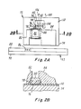
- Figure 1 sets forth a preferred embodiment of the latter wherein the magnetostrictive and piezoelectric films are deposited directly to the gate of an associated MOSFET transistor.
- the IMP-MOS device 10 includes a substrate 12 of P-type silicon in which two zones have been heavily doped to provide N-type regions 14 and 16, respectively.
- insulating Si0 2 regions 18, 20, and 22, respectively On top of the substrate and adjoining the N-type regions 14 and 16 are formed insulating Si0 2 regions 18, 20, and 22, respectively, and on top thereof are deposited metallic contact regions 24, 26, and 28 respectively, thereby completing a conventional MOSFET transistor. Appropriate potentials may be applied to the device such as via conductors 30, 32 and 40 secured to the metallic contacts-24, 26 and 28, respectively.
- the IMP-MOS device of this embodiment is completed by deposition of a piezoelectric film 34 onto the gate contact 26 and by subsequent deposition of a magnetostrictive film 36 onto the piezoelectric film 34. Electrical potentials may be applied to the magnetostrictive film via lead 38 and to the underlying gate electrode 26 via lead 40.
- a short description of the operation of a convention MOSFET device will be useful.
- a potential of suitable magnitude and polarity is applied to the lead 40, a conductive channel is formed between the two N-type regions 14 and 16.
- Application of a voltage between electrodes 30 and 32 results in a current flow between these two electrodes; the magnitude of which is determined by the polarity and magnitude of the potential applied to the lead 40.
- the magnetic field is detected and transduced into an electrical signal, resulting in a modulated potential on the gate electrode 26 in the following manner:
- a magnetic field applied in the plane of the magnetostrictive element 36 produces a fractional length change in this element.
- Equivalent devices to that shown in Figure 1 may be made using either N-channel or P-channel silicon substrates, operating in either an enhancement or depletion mode. If such a device is operated in the depletion mode, no further biasing of the gate electrode is necessary, and appropriate potentials need only be applied to the source and drain electrodes via a potential source, and if desired, appropriate potentials may be applied to the piezoelectric layer for poling via a lead secured to the magnetostrictive layer.
- a device similar to that set forth in Figure 1 was constructed in the following manner.
- a P-channel enhancement mode MOSFET transistor was fabricated from an N-type silicon substrate utilizing conventional MOSFET technology, wherein the gate electrode was prepared having dimensions of approximately 25 by 1,000 micrometers.
- a prototype combination of magnetostrictive and piezoelectric films was formed as follows: A film of commercially available 25-micron thick polyvinylidene fluoride (PVF 2 ) was metallized with a thin film of aluminum on both sides and subsequently poled by heating the PVF 2 to a temperature in excess of its Curie point and allowing it thereafter to cool while in an electric field.
- PVF 2 polyvinylidene fluoride
- the thus poled film was then-mounted via a transfer adhesive to a water cooled rotating substrate in a vacuum chamber of an ion beam deposition system.
- the PVF 2 was then maintained near room temperature through a subsequent deposition operation.
- a magnetostrictive thin film of approximately 500 nanometers of nickel was subsequently ion beam sputtered onto the PVF 2 from a 98%+ pure nickel foil target.
- the nickel coated PVF 2 film was removed and cut into strips approximately 1 by 6 millimeters in cross section.
- a thin layer of silver conductive epoxy was applied to the side of the PVF 2 opposite to that on which the nickel film was deposited.
- the strip was then glued onto the gate of the MOSFET transistor described above, assuring good electrical contact between the bottom layer of the PVF 2 and the metallized gate.
- the top layer of the PVF 2 (that having the nickel film sputtered thereon) served as the outer electrode of the transducer structure and was connected to the substrate ground.
- DC voltage is applied between the source and drain by connecting a source of potential and drain resistor in series with the MOSFET, while a bias voltage is applied to the gate to bias the MOSFET into the saturation region, and also to provide a reasonable value of conductance.
- the AC output of the amplifier is taken from the drain resistor through a coupling capacitor.
- the value of the drain resistor typically about 10 k-ohms, was selected to give high amplifier gain for a reasonable source-drain supply voltage.
- an alternative construction to that described hereinabove was prepared using a blend of PVF 2 and PMMA as the piezoelectric film.
- the polymer blend was first cast onto the gate electrode from a solution in a conventional manner.
- a thin gold layer was subsequently sputtered onto the PVF 2 -PMMA blend to form an outer electrode, primarily to be used for poling purposes.
- the PVF 2 -PMMA film was then poled in situ by applying an intense electrical field gradient thereto, such as by maintaining a 6 KV field across the film for about 10 seconds.
- the MOSFET wafer was then mounted in a conventional integrated circuit chip carrier and wire bonded to bonding pads therein in a conventional manner.
- a length of 0.75 millimeter wide amorphous Fea O B 20 magnetostrictive ribbon was then glued over the gold film on the PVF 2 -PMMA layer with a rigid epoxy so as to provide good strain coupling.
- an IMP-MOS device functionally equivalent to that described hereinabove may be constructed together with suitable high permeability pole pieces to enable remote sensing of localized magnetic fields such as may be present in magnetic recording media.
- One such device is set forth in plane view in Figure 2A and associatedly in cross-sectional view in Figure 2B.
- the device 72 includes a silicon substrate 74 overlaid with an insulator layer 110 onto which is deposited a metal electrode 76. Overlying the metal electrode 76 is a thin-film of piezoelectric material 78, and overlying the piezoelectric layer a thin-film of a magnetostrictive material 80.
- magnetostrictive-piezoelectric films are thus formed within the gap of the pole pieces 82 and 84.
- the pole piece 84 is desirably made sufficiently extensive in area to result in a sufficiently low flux density to avoid magnetically affecting recorded data passing adjacent the pole piece 84.
- the flux thus induced in the magnetostrictive film 80 will produce an associated electrical output from the piezoelectric film in the manner described in conjunction with
- a conventional MOSFET 92 is separately fabricated and bonded to the silicon substrate 74 as there shown.
- the ground electrode 94 may then be coupled to the underlying electrode 76 via lead 96.
- the contact from the magnetostrictive layer 80 may be made to the gate electrode 98 via lead 100.
- appropriate contacts to the source and drain electrodes 102 and 104, respectively, may be made via leads 106 and 108.
- such a device includes the substrate 74 and an insulating layer 110 thereover to prevent shorting out of the electrodes surrounding the piezoelectric layer 78.
- the metal electrode 76 on top of the insulating layer 110 is the metal electrode 76, the piezoelectric film 78 and the magnetostrictive film 80, respectively.
- the high permeability thin-film pole pieces 82 and 84 are similarly shown deposited over the magnetostrictive film, leaving the gap region therebetween.
- another embodiment of the present invention may be utilized with external pole pieces to provide both a read and write capability.
- a device may include a silicon substrate on which are deposited successive thin-films so as to form a single turn inductive winding around appropriate pole pieces, similar to those set forth in Figure 2A and 2B.
- a conventional thin-film write head such as is particularly adapted for recording onto perpendicularly oriented magnetic recording nedia, may then be deposited appropriate films to provide a nagnetostrictive-piezoelectric transducer.
- a thin-film of magnetostrictive material which surrounds the spacer layer and extends into direct contact with the pole tip so as to complete a magnetic circuit therewith.
- a piezoelectric film may next be deposited onto the magnetostrictive film, and an appropriate metallic contact layer applied thereover.
- Such a configured head may thus be utilized in a write mode by applying suitable currents to the inductive winding induce an appropriate magnetic field in the core thereby providing a concentrated field within the pole piece to induce localized magnetic fields within a magnetic recording medium positioned therebelow.
- suitable currents to the inductive winding induce an appropriate magnetic field in the core thereby providing a concentrated field within the pole piece to induce localized magnetic fields within a magnetic recording medium positioned therebelow.
- such localized fields will cause a strain to be induced within the magnetostrictive layer, a flux return path for such fields thereupon being provided via the pole piece.
- the stress induced within the magnetostrictive filia is coupled to the piezoelectric film to cause the production of localized electric charges and associated potentials which are coupled to an associated amplifier.
- a similar alternative embodiment may be constructed utilizing a magnetic material as the underlying substrate, such as a sheet of high permeability material which may then also form the pole piece.
- the piezoelectric thin-film may be applied directly to the magnetic substrate, and would also form the gap otherwise formed by the insulating film, while a separate insulating film would be applied between the magnetic substrate and the overlying magnetostrictive film to prevent shorting out the piezoelectric film sandwiched therebetween.
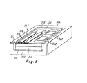
- Figure 3 sets forth in perspective view a further preferred embodiment of the present invention wherein a plurality of magnetostrictive-piezoelectric sensing elements are provided, thus enabling simultaneous playback of parallel tracks.
- a device may also be used to maintain the head positioned over a single track via a dynamic servoing system.
- a head 162 may include a silicon substrate 164 onto which is deposited a metallic electrode 165 and an extended area piezoelectric film 166.
- several discrete magnetostrictive films may then be deposited onto the piezoelectric film 166 such as films 168, 170 and 172.
- each discrete sensor may then be provided to the discrete magnetostrictive films via leads 174, 176, and 178, thus coupling each discrete sensor to an appropriate amplifier (not shown).
- stress separately induced in any one of the magnetostrictive elements 168, 170, and 172, respectively, will induce a localized strain in that portion of the piezoelectric film proximate the particular stressed magnetostrictive element, thereby providing a localized voltage on one of the leads 174, 176, or 178.
- a single piezoelectric film 166 has been utilized, similarly, separate piezoelectric films matching the magnetostrictive films may likewise be used.
- the heads may be utilized to playback three separate recorded tracks on a magnetic recording medium 180 positioned adjacent thereto.
- a servo network may be provided to use the three heads in combination.
- the two servoing elements will have the same output. If the head starts to drift off the track, one of the servoing elements will have an output different from that of the other two elements, and an error signal generated from the asymmetry in the outputs which can be used to activate a servoing network to recenter the head over the track.
- IMP-MOS devices of the present invention are all formed on a common semiconductive substrate.
- An alternative IMP-MOS device may be formed utilizing a totally passive substrate, such as formed of a planar sheet of glass or the like, onto one portion of which may be adhered a conventional MOSFET transistor and onto an adjacent portion may similarly be adhered a second portion of the device formed of a suitable substrate, onto which are deposited a conductive electrode and piezoelectric and magnetostrictive films together with suitable interconnecting electrodes.
- a silicon wafer substrate was utilized as the separate substrate.
- a gold film was first sputtered thereon to serve as a lower electrode.
- the sensing element was then cut into a size suitable to be mounted onto the underlying substrate.
- a common silicon substrate may be provided for both the MOSFET transistor and a separate portion of that substrate reserved for the separate deposition of the magnetostrictive and piezoelectric films. Accordingly, electrical contacts connecting the magnetostrictive and piezoelectric films to the MOSFET transistor may be provided as appropriate.
- a small magnetic signal must be detected in the presence of much stronger noise that is both time varying and/or steady state.
- a further difficulty is sometimes encountered in that various piezoelectric materials are both pressure- sensitive as well as sensitive to other stimuli such as temperature.
- non-magnetically induced strains can also couple unwanted signals via the piezoelectric film.
- Figure 4 sets forth a preferred embodiment of the present invention wherein additional components are provided for suppressing unwanted effects of extraneous stimuli other than that of the main magnetic signals of interest.
- a pair of sensing elements as nearly geometrically identical as possible are provided, with only one of the sensing elements receiving the stimulus of interest, but with both the sensing elements equally receiving all background stimuli.
- a "bridge" configuration is then often used for devices requiring outside power supplies for operation.
- FET's which are voltage variable resistors, would be so configured.
- the present device being magnetoelectric in nature, does not require an external power supply in order to function, such that a pair of devices will suffice. Accordingly, the device set forth in Figure 4 incorporates a common mode noise rejection feature.
- the device 232 includes a common substrate 234 within which are fabricated two separate MOSFET transistors each shown generally extending over two separate regions 236 and 238, respectively, of the substrate.
- MOSFET transistors would be conventional in nature, having the requisite doped regions, metal oxide layers and source, gate, and drain electrodes.
- a base electrode 240 may be deposited onto a third region of the substrate and a piezoelectric film 242 deposited thereover.
- the common mode noise rejection capability is provided by depositing onto different portions of the piezoelectric film 242 a magnetostrictive film 244 and a similarly configured non-magnetostrictive film 246, such as may be provided from a thin-film aluminum, or the like.
- each of the respective films 244 and 246 are then made via leads 248 and 250 to the respective gate electrodes 252 and 254 of the respective MOSFET transistors.
- Appropriate sources of potential and biasing resistors 256 and 258, and 260 and 262, respectively, will also be provided for energization of the two separate MOSFET sections. Similarly, bias supplies will also be provided as appropriate.
- the output from the two respective MOSFET sections will then typically be coupled to a differential amplifier 264 to provide an appropriate differential output signal.
- a ZnO thin-film such as element 242 would be sputtered onto the conductor 240 and a film of FeSi deposited as the magnetostrictive film 244, while an aluminum film is sputtered as layer 246.
- the second film 246 is desirably dimensionally identical to that of the magnetostrictive film and should be positioned close to it.
- common mode noise rejection may be obtained even though both the films 244 and 246 are magnetostrictive in nature.
- only one of the films would be exposed to a signal field, with appropriate shielding provided if desired to minimize cross-talk.
- the transducer then electrically consists of two capacitors sharing a common piezoelectric dielectric and ground electrode. While the two capacitors are electrically identical, only one of which responds to the stimulus of interest. Hence, the difference between the outputs of the two will represent a magnetically induced signal with common mode noise rejected.
- such a structure may also be built with the respective magnetostrictive and non-magnetostrictive films fabricated directly on the gates of the two separate MOSFETs.
- a common mode noise rejection may similarly be achieved using a single MOSFET device by connecting magnetically active and magnetically-inactive transducers in series with the gate of the MOSFET.
- a single MOSFET device may be fabricated using a single silicon substrate on a first portion of which is fabricated a conventional MOSFET transistor similar to that set forth in regions 236 and 238 in Figure 4.
- the piezoelectric film may be applied similarly configured magnetostrictive films and non-magnetostrictive films, such as a thin-film of aluminum.
- the aluminum film may similarly be grounded, while the magnetostrictive film is coupled to the gate electrode of the MOSFET transistor.
- the lower electrode is left floating such that the piezoelectric film essentially forms two capacitors in series, the first capacitor being formed by the piezoelectric film between the aluminum film and the lower electrode, and the second capacitor being formed between the electrode and the magnetostrictive film.
- one such device 304 may include a conventional ceramic chip carrier 306 which carrier is arranged to have an internal recess and to be open at one end 308.
- chip carriers typically have a plurality of bonding pads positioned about the periphery of the carrier for enabling electrical connections to be made to the various portions of a semiconductor substrate positioned therein.
- a silicon substrate 310 may be mounted with an appropriate thermally conductive adhesive within the carrier 306, one end of the substrate terminating substantially parallel with the open end of the carrier 308. Over the entire silicon substrate 310 may be sputtered a thin film 312 of gold approximately 500 nanometers thick.
- a magnetostrictive film 314 and a non-magnetostrictive film 316 may be deposited over the Z nO film.
- the magnetostrictive film may be a thin-film of an iron-silicon alloy such as Fe 72 Si 28 , having a thickness of approximately 500 nanometers and a cross-sectional area of approximately 1 x 5 millimeters.
- the non-magnetostrictive film 316 may be a sputtered film of aluminum having a thickness of approximately 300 to 500 nanometers, and of similar physical dimensions.
- the magnetostrictive and non-magnetostrictive films 314 and 316 may be coupled to the electrodes of integrated MOSFET transistors 322 and 324.
- the MOSFETs are bonded to another portion of the zinc oxide piezoelectric film 313 via a suitable thermally conductive adhesive.
- the periphery of the chip carrier 306 will include bonding pads (not shown) such that connections to appropriate biasing potentials and input and/or output signals may be made to the MOSFETs.
- Such a chip carrier with the respective film terminating proximate the open end of the carrier may be utilized to detect perpendicularly encoded localized magnetic field patterns within a magnetic recording medium.
- a localized bit comes proximate the magnetostrictive and metallic films 314 and 316, respectively, differential stress will be induced within the magnetostrictive film to provide an appropriate signal from the MOSFETs as the medium is caused to move thereby.
- the amplifier which forms an integrated part of the device of the present invention is desirably a MOSFET type transistor and provides the first stage of amplification, as well as impedance matching, to the magnetostrictive-piezoelectric portion of the device.
- the integrated transistor In order to yield the optimum output for the sensor as a whole, the integrated transistor should have a small gate capacitance and a high transconductance. MOSFET type transistors are thus attractive choices for the present application due to their high input impedance and electrical isolation which make it well matched to the magnetostrictive-piezoelectric sensor.
- alternative amplifier constructions such as JFET's and the like would also be suitable.
- the MOS transistors desirably used in the present devices can be fabricated by standard IC processes. Either N-channel or P-channel devices may be used. However, N-channel devices are particularly attractive as they generally yield higher transconductances than do equivalent geometry P-channel type devices. Also, either enhancement or depletion mode devices can be used, depending upon the particular applications intended.
- the capacitance at the gate of the transistor be as low as feasible. This desirability results from the nature of the magnetostrictive-piezoelectric transducer which generates a fixed charge which must be distributed over its own capacitance as well as over all parallel capacitances, including that of the MOSFET gate. Minimizing the parallel capacitances results in the maximum output signal.
- piezoelectric materials may be suitably utilized in the thin-film piezoelectric layer.
- such materials are ZnO, PVF 2 , CdS, and PZT ceramics.
- the piezoelectric thin-film is applied in a manner which results in a high piezoelectric coefficient.
- Optimum thicknesses and methods of application will depend upon the particular material selected.
- ZnO and CdS may be sputtered onto the gate of the MOSFET.
- PVF 2 may either be glued from a thin sheet form or cast from a solution and poled in situ on the gate of the transistor.
- An important consideration is that there must be good electrical contact between the piezoelectric material and the gate electrode.
- the material selected must have high resistivity and good electro-mechanical coupling constant.
- such a layer is desirably deposited in intimate contact with the piezoelectric film.
- a number of materials may be used as magnetotrictive elements.
- optimum thicknesses and application techniques will depend upon the particular material selected, there being a variety of techniques available for providing the coupling between the magnetostrictive and piezoelectric films.
- the magnetostrictive material may be sputtered, evaporated, plated, or even adhered with a thin epoxy layer onto the piezoelectric material.
- the mechanical and electrical characteristics of the device will depend on the particular deposition or application method employed.
- magnetostrictive film that actually couples to a magnetic field. Consequently, its properties are perhaps the most critical.
- the basic material characteristics required are relatively low coercivity, so that the film magnetization can be easily switched, and a relatively high magnetostriction coefficient.
- the particular properties of the magnetostrictive layer can be tailored somewhat to match the properties of the piezoelectric layer and the MOSFET being used. However, in general, it is desirable to have the highest possible induced strain per unit applied field, consistent with achieving magnetic saturation at an acceptably low field intensity.
- the physical dimensions of the film determine the spatial field resolution and bandwidth of the sensor. Thin film, photolithographically patterned elements will display maximum bandwidth and resolution.
Landscapes
- Engineering & Computer Science (AREA)
- Manufacturing & Machinery (AREA)
- Hall/Mr Elements (AREA)
- Magnetic Heads (AREA)
- Recording Or Reproducing By Magnetic Means (AREA)
Priority Applications (1)
| Application Number | Priority Date | Filing Date | Title |
|---|---|---|---|
| AT83301491T ATE37248T1 (de) | 1982-04-13 | 1983-03-17 | Integrierter, magnetostriktiver-piezoelektrischer mos-lese-magnetkopf. |
Applications Claiming Priority (2)
| Application Number | Priority Date | Filing Date | Title |
|---|---|---|---|
| US06/368,025 US4520413A (en) | 1982-04-13 | 1982-04-13 | Integrated magnetostrictive-piezoelectric-metal oxide semiconductor magnetic playback head |
| US368025 | 1982-04-13 |
Publications (2)
| Publication Number | Publication Date |
|---|---|
| EP0091739A1 true EP0091739A1 (fr) | 1983-10-19 |
| EP0091739B1 EP0091739B1 (fr) | 1988-09-14 |
Family
ID=23449581
Family Applications (1)
| Application Number | Title | Priority Date | Filing Date |
|---|---|---|---|
| EP83301491A Expired EP0091739B1 (fr) | 1982-04-13 | 1983-03-17 | Tête magnétique de lecture intégrée, magnétostrictive-piézoélectrique MOS |
Country Status (9)
| Country | Link |
|---|---|
| US (1) | US4520413A (fr) |
| EP (1) | EP0091739B1 (fr) |
| JP (1) | JPS58188321A (fr) |
| KR (1) | KR920004215B1 (fr) |
| AT (1) | ATE37248T1 (fr) |
| CA (1) | CA1193361A (fr) |
| DE (1) | DE3378004D1 (fr) |
| HK (1) | HK94489A (fr) |
| SG (1) | SG19689G (fr) |
Cited By (4)
| Publication number | Priority date | Publication date | Assignee | Title |
|---|---|---|---|---|
| EP0103352A3 (en) * | 1982-07-14 | 1985-10-23 | Minnesota Mining And Manufacturing Company | Magnetic sensor, particularly playback head for magnetic recording media |
| EP0173977A3 (fr) * | 1984-09-04 | 1987-05-27 | Honeywell Inc. | Tête d'enregistrement magnétostrictive |
| EP3340323A1 (fr) * | 2016-12-22 | 2018-06-27 | Melexis Technologies NV | Dispositif à semi-conducteurs comprenant une structure de transducteur magnétoélectrique passive |
| EP3917009A1 (fr) * | 2020-05-29 | 2021-12-01 | Melexis Bulgaria Ltd. | Dispositif à semi-conducteurs comprenant un transducteur magnéto-électrique passif |
Families Citing this family (28)
| Publication number | Priority date | Publication date | Assignee | Title |
|---|---|---|---|---|
| JPS60253958A (ja) * | 1984-05-31 | 1985-12-14 | Sharp Corp | センサ |
| JPS61104313A (ja) * | 1984-10-22 | 1986-05-22 | Sharp Corp | 薄膜磁気ヘツド装置 |
| JPS63106910A (ja) * | 1986-10-24 | 1988-05-12 | Hitachi Ltd | 薄膜磁気ヘツド |
| US4918655A (en) * | 1988-02-29 | 1990-04-17 | Honeywell Inc. | Magnetic device integrated circuit interconnection system |
| US5254504A (en) * | 1989-04-13 | 1993-10-19 | Trustees Of The University Of Pennsylvania | Method of manufacturing ferroelectric MOSFET sensors |
| US5514899A (en) * | 1994-05-11 | 1996-05-07 | Hong Kong University Of Science And Technology | Dual-emitter lateral magnetometer |
| DE19622415A1 (de) * | 1996-06-04 | 1997-12-11 | Siemens Ag | CMOS-Halbleiterstruktur und Verfahren zur Herstellung derselben |
| US6060755A (en) * | 1999-07-19 | 2000-05-09 | Sharp Laboratories Of America, Inc. | Aluminum-doped zirconium dielectric film transistor structure and deposition method for same |
| JP2004015768A (ja) * | 2002-06-12 | 2004-01-15 | Murata Mfg Co Ltd | 圧電型電気音響変換器 |
| JP2007141977A (ja) * | 2005-11-16 | 2007-06-07 | Matsushita Electric Ind Co Ltd | 半導体装置 |
| US7345475B2 (en) * | 2006-03-17 | 2008-03-18 | University Of Maryland | Ultrasensitive magnetoelectric thin film magnetometer and method of fabrication |
| KR100909962B1 (ko) * | 2006-05-10 | 2009-07-29 | 삼성전자주식회사 | 전계 정보 재생 헤드, 전계 정보 기록/재생헤드 및 그제조방법과 이를 채용한 정보저장장치 |
| US7706103B2 (en) * | 2006-07-25 | 2010-04-27 | Seagate Technology Llc | Electric field assisted writing using a multiferroic recording media |
| KR100773556B1 (ko) * | 2006-08-02 | 2007-11-07 | 삼성전자주식회사 | 전계 재생/기록 헤드와 그의 제조방법 및 전계 재생/기록헤드를 포함한 정보 재생/기록 장치 |
| KR100763926B1 (ko) * | 2006-10-09 | 2007-10-05 | 삼성전자주식회사 | 정보 기록 매체, 정보 기록 매체의 제조방법, 기록/재생헤드 및 기록/재생 헤드의 제조방법 |
| US20080143519A1 (en) * | 2006-12-19 | 2008-06-19 | 3M Innovative Properties Company | Tamper-indicating radio frequency identification tag and methods of indicating tampering of a radio frequency identification tag |
| US7948713B2 (en) * | 2007-01-12 | 2011-05-24 | Tdk Corporation | Magnetic head slider using giant magnetostrictive material |
| US8587902B2 (en) * | 2007-04-12 | 2013-11-19 | International Business Machines Corporation | Device select system for multi-device electronic system |
| US9300284B2 (en) | 2007-04-12 | 2016-03-29 | Globalfoundries Inc. | Device select system for multi-device electronic system |
| AU2009268439B2 (en) * | 2008-07-11 | 2013-12-05 | Brain Basket, LLC | Magnetostrictive auditory system |
| US20110137184A1 (en) * | 2008-08-19 | 2011-06-09 | Fan Ren | Pressure sensing |
| JP5678727B2 (ja) * | 2011-03-03 | 2015-03-04 | セイコーエプソン株式会社 | 振動デバイス、振動デバイスの製造方法、電子機器 |
| WO2013052846A1 (fr) | 2011-10-06 | 2013-04-11 | Brain Basket, LLC | Dispositif d'audibilité et de compréhension auditive |
| WO2016066723A1 (fr) * | 2014-10-28 | 2016-05-06 | Katholieke Universiteit Leuven | Machines électriques |
| CN108054273B (zh) * | 2017-12-28 | 2024-03-08 | 中国科学院宁波材料技术与工程研究所 | 一种场效应晶体管式磁传感器、其制备方法与使用方法 |
| CN108039406B (zh) * | 2017-12-28 | 2024-03-08 | 中国科学院宁波材料技术与工程研究所 | 一种磁传感器、其制备方法与使用方法 |
| CN110729396B (zh) * | 2019-09-25 | 2022-09-16 | 郑州轻工业学院 | 一种具有自放大能力的磁电薄膜传感器 |
| CN119135113B (zh) * | 2024-11-06 | 2025-01-28 | 北京量子信息科学研究院 | 基于半导体薄膜材料的机械振子量子器件及其制备方法以及读取装置 |
Citations (6)
| Publication number | Priority date | Publication date | Assignee | Title |
|---|---|---|---|---|
| US2683856A (en) * | 1951-01-24 | 1954-07-13 | Clevite Corp | Magnetic-electric transducer |
| US3389230A (en) * | 1967-01-06 | 1968-06-18 | Hudson Magiston Corp | Semiconductive magnetic transducer |
| US3553540A (en) * | 1967-03-13 | 1971-01-05 | Ncr Co | Magnetic-field-sensing field-effect transistor |
| US3800193A (en) * | 1972-09-05 | 1974-03-26 | Ibm | Magnetic sensing device |
| FR2321169A1 (fr) * | 1975-08-14 | 1977-03-11 | Ibm | Tetes de lecture magnetoresistives pour operations d'asservissement |
| US4048648A (en) * | 1976-06-30 | 1977-09-13 | International Business Machines Corporation | High carrier velocity fet magnetic sensor |
Family Cites Families (10)
| Publication number | Priority date | Publication date | Assignee | Title |
|---|---|---|---|---|
| US3344237A (en) * | 1967-09-26 | Desposited film transducing apparatus and method op producing the apparatus | ||
| US3987485A (en) * | 1973-02-20 | 1976-10-19 | Matsushita Electric Industrial Co., Ltd. | Magnetic head with thin film components |
| US3909809A (en) * | 1973-12-17 | 1975-09-30 | Canadian Patents Dev | Magnetic bubble domain sensing device |
| US3908194A (en) * | 1974-08-19 | 1975-09-23 | Ibm | Integrated magnetoresistive read, inductive write, batch fabricated magnetic head |
| JPS5278412A (en) * | 1975-12-25 | 1977-07-01 | Nec Corp | Magnetic head |
| JPS6022407B2 (ja) * | 1976-01-20 | 1985-06-01 | 日本電気株式会社 | 磁気ヘツド |
| US4129880A (en) * | 1977-07-01 | 1978-12-12 | International Business Machines Incorporated | Channel depletion boundary modulation magnetic field sensor |
| JPS5891B2 (ja) * | 1977-09-30 | 1983-01-05 | 俊一 岩崎 | 磁気記録媒体 |
| FR2443733A1 (fr) * | 1978-12-08 | 1980-07-04 | Thomson Csf | Tete de lecture magnetique et lecteur muni d'une telle tete |
| DE3002783A1 (de) * | 1980-01-26 | 1981-07-30 | Standard Elektrik Lorenz Ag, 7000 Stuttgart | Sensoranordnung |
-
1982
- 1982-04-13 US US06/368,025 patent/US4520413A/en not_active Expired - Lifetime
-
1983
- 1983-03-17 EP EP83301491A patent/EP0091739B1/fr not_active Expired
- 1983-03-17 DE DE8383301491T patent/DE3378004D1/de not_active Expired
- 1983-03-17 AT AT83301491T patent/ATE37248T1/de not_active IP Right Cessation
- 1983-04-12 JP JP58063132A patent/JPS58188321A/ja active Pending
- 1983-04-12 CA CA000425672A patent/CA1193361A/fr not_active Expired
- 1983-04-13 KR KR1019830001537A patent/KR920004215B1/ko not_active Expired
-
1989
- 1989-03-31 SG SG196/89A patent/SG19689G/en unknown
- 1989-11-30 HK HK944/89A patent/HK94489A/en not_active IP Right Cessation
Patent Citations (6)
| Publication number | Priority date | Publication date | Assignee | Title |
|---|---|---|---|---|
| US2683856A (en) * | 1951-01-24 | 1954-07-13 | Clevite Corp | Magnetic-electric transducer |
| US3389230A (en) * | 1967-01-06 | 1968-06-18 | Hudson Magiston Corp | Semiconductive magnetic transducer |
| US3553540A (en) * | 1967-03-13 | 1971-01-05 | Ncr Co | Magnetic-field-sensing field-effect transistor |
| US3800193A (en) * | 1972-09-05 | 1974-03-26 | Ibm | Magnetic sensing device |
| FR2321169A1 (fr) * | 1975-08-14 | 1977-03-11 | Ibm | Tetes de lecture magnetoresistives pour operations d'asservissement |
| US4048648A (en) * | 1976-06-30 | 1977-09-13 | International Business Machines Corporation | High carrier velocity fet magnetic sensor |
Non-Patent Citations (9)
| Title |
|---|
| IBM TECHNICAL DISCLOSURE BULLETIN, vol. 16, no. 8, January 1974, pages 2491-2492, Armonk, New York, USA * |
| IBM TECHNICAL DISCLOSURE BULLETIN, vol. 18, no. 1, June 1975, page 24, Armonk, New York, USA * |
| IBM TECHNICAL DISCLOSURE BULLETIN, vol. 8, no. 3, August 1965, pages 359-360, Armonk, New York, USA * |
| IBM TECHNICAL DISCLOSURE BULLETIN; vol. 17, no. 11, April 1975, pages 3478-3480, Armonk, New York, USA * |
| IBM TECHNICAL DISCLOSURE BULLETIN; vol. 17, no. 7, December 1974, page 1862, Armonk, New York, USA * |
| INTERNATIONAL JOURNAL OF ELECTRONICS, vol. 51, no. 3, September 1981, pages 255-262, Basingstoke, Hampshire, GB. * |
| PATENTS ABSTRACTS OF JAPAN * |
| PATENTS ABSTRACTS OF JAPAN, vol. 1, no. 148, 29th November 1977, page 7660 E 77 & JP - A - 52 88317 (NIPPON DENKI K.K.) 23-07-1977 * |
| PATENTS ABSTRACTS OF JAPAN, vol. 4, no. 172 (P-38)[654], 27th November 1980 & JP - A - 55 117 729 (MATSUSHITA DENKI SANGYO K.K.) 10-09-1980 * |
Cited By (8)
| Publication number | Priority date | Publication date | Assignee | Title |
|---|---|---|---|---|
| EP0103352A3 (en) * | 1982-07-14 | 1985-10-23 | Minnesota Mining And Manufacturing Company | Magnetic sensor, particularly playback head for magnetic recording media |
| EP0173977A3 (fr) * | 1984-09-04 | 1987-05-27 | Honeywell Inc. | Tête d'enregistrement magnétostrictive |
| EP3340323A1 (fr) * | 2016-12-22 | 2018-06-27 | Melexis Technologies NV | Dispositif à semi-conducteurs comprenant une structure de transducteur magnétoélectrique passive |
| CN108231997A (zh) * | 2016-12-22 | 2018-06-29 | 迈来芯保加利亚有限公司 | 包括无源磁电式换能器结构的半导体器件 |
| CN108231997B (zh) * | 2016-12-22 | 2020-12-29 | 迈来芯保加利亚有限公司 | 包括无源磁电式换能器结构的半导体器件 |
| US11527705B2 (en) | 2016-12-22 | 2022-12-13 | Melexis Bulgaria Ltd. | Semiconductor device comprising passive magnetoelectric transducer structure |
| EP3917009A1 (fr) * | 2020-05-29 | 2021-12-01 | Melexis Bulgaria Ltd. | Dispositif à semi-conducteurs comprenant un transducteur magnéto-électrique passif |
| US12046685B2 (en) | 2020-05-29 | 2024-07-23 | Melexis Bulgaria Ltd | Semiconductor device with passive magneto-electric transducer |
Also Published As
| Publication number | Publication date |
|---|---|
| JPS58188321A (ja) | 1983-11-02 |
| KR840004809A (ko) | 1984-10-24 |
| ATE37248T1 (de) | 1988-09-15 |
| KR920004215B1 (ko) | 1992-05-30 |
| EP0091739B1 (fr) | 1988-09-14 |
| DE3378004D1 (en) | 1988-10-20 |
| HK94489A (en) | 1989-12-08 |
| CA1193361A (fr) | 1985-09-10 |
| SG19689G (en) | 1989-09-01 |
| US4520413A (en) | 1985-05-28 |
Similar Documents
| Publication | Publication Date | Title |
|---|---|---|
| US4520413A (en) | Integrated magnetostrictive-piezoelectric-metal oxide semiconductor magnetic playback head | |
| US4499515A (en) | Integrated magnetostrictive-piezoresistive magnetic recording playback head | |
| US4356523A (en) | Narrow track magnetoresistive transducer assembly | |
| JPH03505501A (ja) | 磁気抵抗による垂直記録用の磁気読取りヘッド及び当該ヘッドの製造方法 | |
| JPH06267026A (ja) | 半導体磁界検知磁気ヘッドの製造方法およびそれにより製造される半導体磁界検知磁気ヘッド | |
| JPH07502365A (ja) | 集積バイアス及び磁気シールド層を有する磁気抵抗性ヘッド | |
| JPS61120318A (ja) | 一体化薄膜磁気ヘツド | |
| JPS6177114A (ja) | 磁気抵抗効果型磁気ヘツド | |
| JPS61178710A (ja) | 薄膜磁気ヘツド及びその製造方法 | |
| US6028749A (en) | Magnetic head having a multilayer structure and method of manufacturing the magnetic head | |
| JP2907148B2 (ja) | 強磁性トンネル効果膜を用いた磁気抵抗効果素子及びその製造方法 | |
| US3291918A (en) | Magneto-electric signal transmission system | |
| JP3285094B2 (ja) | 薄膜磁気ヘッドの研磨方法 | |
| JP2507710B2 (ja) | ヨ−ク型薄膜磁気ヘツド | |
| JP2878738B2 (ja) | 記録再生兼用薄膜磁気ヘッド | |
| JP2747034B2 (ja) | 磁気抵抗効果ヘッド | |
| JPS60150222A (ja) | 薄膜磁気ヘツド | |
| JPS626420A (ja) | 薄膜磁気ヘツド | |
| JPS60202513A (ja) | 磁気抵抗効果型マルチ磁気ヘツドの製造方法 | |
| JPS58224430A (ja) | 混成薄膜集積ヘツド | |
| JPS62197909A (ja) | 磁気ヘツドおよびその製造方法 | |
| JPS6113413A (ja) | 薄膜型磁気ヘツド装置 | |
| JPH0376535B2 (fr) | ||
| JPH028468B2 (fr) | ||
| JPS5857618A (ja) | 薄膜磁気ヘツド |
Legal Events
| Date | Code | Title | Description |
|---|---|---|---|
| PUAI | Public reference made under article 153(3) epc to a published international application that has entered the european phase |
Free format text: ORIGINAL CODE: 0009012 |
|
| AK | Designated contracting states |
Designated state(s): AT DE FR GB IT NL |
|
| 17P | Request for examination filed |
Effective date: 19840412 |
|
| ITF | It: translation for a ep patent filed | ||
| GRAA | (expected) grant |
Free format text: ORIGINAL CODE: 0009210 |
|
| AK | Designated contracting states |
Kind code of ref document: B1 Designated state(s): AT DE FR GB IT NL |
|
| REF | Corresponds to: |
Ref document number: 37248 Country of ref document: AT Date of ref document: 19880915 Kind code of ref document: T |
|
| REF | Corresponds to: |
Ref document number: 3378004 Country of ref document: DE Date of ref document: 19881020 |
|
| ET | Fr: translation filed | ||
| PLBE | No opposition filed within time limit |
Free format text: ORIGINAL CODE: 0009261 |
|
| STAA | Information on the status of an ep patent application or granted ep patent |
Free format text: STATUS: NO OPPOSITION FILED WITHIN TIME LIMIT |
|
| 26N | No opposition filed | ||
| ITTA | It: last paid annual fee | ||
| PGFP | Annual fee paid to national office [announced via postgrant information from national office to epo] |
Ref country code: FR Payment date: 19970213 Year of fee payment: 15 |
|
| PGFP | Annual fee paid to national office [announced via postgrant information from national office to epo] |
Ref country code: AT Payment date: 19970217 Year of fee payment: 15 |
|
| PGFP | Annual fee paid to national office [announced via postgrant information from national office to epo] |
Ref country code: NL Payment date: 19970218 Year of fee payment: 15 |
|
| PGFP | Annual fee paid to national office [announced via postgrant information from national office to epo] |
Ref country code: DE Payment date: 19970225 Year of fee payment: 15 |
|
| PGFP | Annual fee paid to national office [announced via postgrant information from national office to epo] |
Ref country code: GB Payment date: 19970226 Year of fee payment: 15 |
|
| PG25 | Lapsed in a contracting state [announced via postgrant information from national office to epo] |
Ref country code: GB Free format text: LAPSE BECAUSE OF NON-PAYMENT OF DUE FEES Effective date: 19980317 Ref country code: AT Free format text: LAPSE BECAUSE OF NON-PAYMENT OF DUE FEES Effective date: 19980317 |
|
| PG25 | Lapsed in a contracting state [announced via postgrant information from national office to epo] |
Ref country code: FR Free format text: THE PATENT HAS BEEN ANNULLED BY A DECISION OF A NATIONAL AUTHORITY Effective date: 19980331 |
|
| PG25 | Lapsed in a contracting state [announced via postgrant information from national office to epo] |
Ref country code: NL Free format text: LAPSE BECAUSE OF NON-PAYMENT OF DUE FEES Effective date: 19981001 |
|
| GBPC | Gb: european patent ceased through non-payment of renewal fee |
Effective date: 19980317 |
|
| NLV4 | Nl: lapsed or anulled due to non-payment of the annual fee |
Effective date: 19981001 |
|
| PG25 | Lapsed in a contracting state [announced via postgrant information from national office to epo] |
Ref country code: DE Free format text: LAPSE BECAUSE OF NON-PAYMENT OF DUE FEES Effective date: 19981201 |
|
| REG | Reference to a national code |
Ref country code: FR Ref legal event code: ST |