EP0091967A1 - Schaltung zur trennung des trägerfrequenzfarbsignals - Google Patents
Schaltung zur trennung des trägerfrequenzfarbsignals Download PDFInfo
- Publication number
- EP0091967A1 EP0091967A1 EP82903184A EP82903184A EP0091967A1 EP 0091967 A1 EP0091967 A1 EP 0091967A1 EP 82903184 A EP82903184 A EP 82903184A EP 82903184 A EP82903184 A EP 82903184A EP 0091967 A1 EP0091967 A1 EP 0091967A1
- Authority
- EP
- European Patent Office
- Prior art keywords
- circuit
- signal
- carrier chrominance
- supplied
- chrominance signal
- Prior art date
- Legal status (The legal status is an assumption and is not a legal conclusion. Google has not performed a legal analysis and makes no representation as to the accuracy of the status listed.)
- Granted
Links
Images



Classifications
-
- H—ELECTRICITY
- H04—ELECTRIC COMMUNICATION TECHNIQUE
- H04N—PICTORIAL COMMUNICATION, e.g. TELEVISION
- H04N9/00—Details of colour television systems
- H04N9/77—Circuits for processing the brightness signal and the chrominance signal relative to each other, e.g. adjusting the phase of the brightness signal relative to the colour signal, correcting differential gain or differential phase
- H04N9/78—Circuits for processing the brightness signal and the chrominance signal relative to each other, e.g. adjusting the phase of the brightness signal relative to the colour signal, correcting differential gain or differential phase for separating the brightness signal or the chrominance signal from the colour television signal, e.g. using comb filter
Definitions
- This invention relates to such a technique that in a comb filter for separating a carrier chrominance signal from a color video signal, even if the carrier chrominance signal contains portions having no vertical correlation, the carrier chrominance signal can be correctly extracted.
- a comb filter is known as a filter for separating a luminance signal and a carrier chrominance signal from a color video signal. Further, a comb filter has been proposed which can avoid a dot interference and a cross color.
- Fig. 1 is a block diagram showing an example thereof.
- a color video signal, or a composed signal (Y L + Y H + C) consisting of a low frequency band component Y L and a high frequency band component Y H of a luminance signal Y and a carrier chrominance signal C is supplied to a terminal 1.
- the signal (Y L + Y H + C) is supplied to a band-pass filter 2 which passes therethrough a signal (Y H + C).
- This signal (Y H + C) and the signal (Y L + Y H + C) are both supplied to a subtracting circuit 3 from which is derived the low frequency band component Y L .
- This low frequency band component Y is supplied through a phase compensation delay circuit 4 to an adding circuit 5.
- the signal (Y H + C) from the filter 2 is supplied to a delay circuit 6 and delayed by one horizontal period so that the delay circuit 6 delivers a signal (Y H - C) consisting of the high frequency band component Y H of one horizontal period before and a carrier chrominance singal -C of opposite phase.
- the signal (Y H - C) and the signal (Y H + C) from the filter 2 are supplied to an amplitude correlating circuit 7.
- the correlating circuit 7 is an analog-AND circuit the example of which will be described later.
- this circuit When this circuit is supplied with two signals Sa and Sb as, for example, shown in Fig. 4A, it produces correlated portions (hatched areas) of both the signals Sa and Sb as shown in Fig. 4F. Accordingly, the correlating circuit 7 delivers the high frequency band component Y H .
- the signal (Y H - C) from the delay circuit 6 is supplied further to an inverter 8 from which a signal (-Y H + C) of inverted phase is derived.
- the signal (-Y H + C) and the signal (Y H + C) from the filter 2 are supplied to a correlating circuit 9 which delivers the carrier chrominance signal C to a terminal 12.
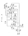
- Fig. 3 is a circuit diagram showing an example of the correlating circuits7 and 9.
- transistors Q 1 and Q 2 When the signals Sa and Sb as shown in Fig. 4A are supplied to terminals Ta and Tb, transistors Q 1 and Q 2 generate a signal Sm as shown in Fig. 4B so that from transistors Q 3 and Q 4 is derived a portion Sn corresponding to the correlated portion of the negative half cycle period of the signals Sa and Sb as shown in Fig. 4C.
- transistors Q 5 and Q 6 is derived a signal Sp as shown in Fig. 4D
- transistors Q 7 and Q produce a correlated portion S q corresponding to a positive half cycle period of the signals Sa and Sb as shown in Fig. 4E.
- the correlated portions between the signals Sa and Sb namely, a correlated signal (Sa A Sb) shown in Fig. 4F is delivered to a terminal Tc.
- the luminance signal Y and the carrier chrominance signal C can be separated from the color video signal.
- no dot interference and no cross color occur.
- the carrier chrominance signal C in the color video signal supplied to the terminal 1 is that as shown in Fig. 2A, or only lines (n + 1) to (n + 4) thereof are colored, the carrier chrominance signals C at the respective circuit elements become as shown in Figs. 2A to 2C and the carrier chrominance signal C which will appear at the terminal 12 becomes as shown in Fig. 2D.
- the carrier chrominance signal C on the line (n + 1) having no vertical correlation is lost or attenuated.
- a mixed signal containing the carrier chrominance signal C is supplied to a delay circuit and delayed one horizontal period.
- This delayed signal and an original color video signal are supplied to a substracting circuit.
- the subtracted output therefrom and the color video signal are supplied to an amplitude correlating circuit from which is derived the carrier chrominance signal C.
- Figs. 1 to 4 and Fig. 6 are respectively diagrams useful for explaining this invention, and Figs. 5 and 7 are respectively systematic diagrams of embodiments according to this invention.
- Reference numeral 2 represents the band-pass filter, 6 the delay circuit, and 9 the amplitude correlating circuit.
- Fig. 5 is a block diagram showing an embodiment of this invention.
- a color video signal (Y L + y H + C) is supplied through a terminal 1 to a band-pass filter 2 from which is derived a mixed signal (Y H + C) of a high frequency band component Y and a carrier chrominance signal C.
- the signal (Y H + C) is supplied to a subtracting circuit 14 and a delay circuit 6 from which a signal (Y H - C) of one horizontal period before is derived.
- This signal (Y H - C) is supplied to the subtracting circuit 14 from which is derived a carrier chrominance signal C.
- the signal C is supplied to a correlating circuit 9 and the signal (Y H + C) from the filter 2 is supplied to the correlating circuit 9 so that the carrier chrominance signal C is delivered therefrom which is then fed to a terminal 12.
- the signal (Y L + Y H + C) fed to the terminal 1 is supplied through a phase compensation delay circuit 4 to a subtracting circuit 15 and the carrier chrominance signal C from the correlating circuit 9 is also supplied to the subtracting circuit 15 from which is derived a luminance signal Y which is then delivered to a terminal 11.
- the carrier chrominance signal C in the color video signal supplied to the terminal 1 is that as shown in Fig. 6A (this is the same as that of Fig. 2A)
- the signal C from the filter 2 becomes as shown in Fig. 6A, too. Therefore, the signal C from the delay circuit 6 becomes that as shown in Fig. 6B and the signal C from the subtracting circuit 14 becomes that as shown in Fig. 6C.
- the correlated output therefrom becomes the carrier chrominance signal C with the original level on the lines (n + 1) to (n + 4) as shown in Fig. 6D.
- the luminance signal Y and the carrier chrominance signal C can be separated from the color video signal. Also, at that time, even if the carrier chrominance signal C includes the portion which has no vertical correlation, the carrier chrominance signal will never be lost or attenuated.
- the circuit arrangement therefor is made simple.
- the delay circuit 6 used is such one which has the characteristic similar to that of the band-pass filter 2 so that the delay circuit 6 is constructed at low cost.
Landscapes
- Engineering & Computer Science (AREA)
- Multimedia (AREA)
- Signal Processing (AREA)
- Processing Of Color Television Signals (AREA)
Applications Claiming Priority (2)
| Application Number | Priority Date | Filing Date | Title |
|---|---|---|---|
| JP169909/81 | 1981-10-23 | ||
| JP56169909A JPS5871783A (ja) | 1981-10-23 | 1981-10-23 | 分離回路 |
Publications (3)
| Publication Number | Publication Date |
|---|---|
| EP0091967A1 true EP0091967A1 (de) | 1983-10-26 |
| EP0091967A4 EP0091967A4 (de) | 1985-12-19 |
| EP0091967B1 EP0091967B1 (de) | 1989-03-22 |
Family
ID=15895209
Family Applications (1)
| Application Number | Title | Priority Date | Filing Date |
|---|---|---|---|
| EP82903184A Expired EP0091967B1 (de) | 1981-10-23 | 1982-10-21 | Schaltung zur trennung des trägerfrequenzfarbsignals |
Country Status (7)
| Country | Link |
|---|---|
| US (1) | US4570177A (de) |
| EP (1) | EP0091967B1 (de) |
| JP (1) | JPS5871783A (de) |
| DE (1) | DE3249132T1 (de) |
| GB (1) | GB2120496B (de) |
| NL (1) | NL8220384A (de) |
| WO (1) | WO1983001554A1 (de) |
Cited By (3)
| Publication number | Priority date | Publication date | Assignee | Title |
|---|---|---|---|---|
| EP0146129A3 (de) * | 1983-12-15 | 1987-12-02 | Sony Corporation | Gerät für die Aufzeichnung und Wiedergabe eines Videosignals |
| EP0281709A1 (de) * | 1987-01-12 | 1988-09-14 | Crosfield Electronics Limited | Verfahren zur Verbesserung eines Farbvideobildes und entsprechende Vorrichtung |
| EP0186514A3 (en) * | 1984-12-25 | 1988-11-30 | Matsushita Electric Industrial Co., Ltd. | Comb filter |
Families Citing this family (8)
| Publication number | Priority date | Publication date | Assignee | Title |
|---|---|---|---|---|
| DE3343261A1 (de) * | 1983-11-30 | 1985-06-05 | Robert Bosch Gmbh, 7000 Stuttgart | Schaltung zur verminderung des farbnebensprechens in einem farbfernsehcoder |
| CA1243398A (en) * | 1985-01-14 | 1988-10-18 | Nec Corporation | Luminance/chrominance separating apparatus |
| US4616254A (en) * | 1985-04-18 | 1986-10-07 | Rca Corporation | Hanging dot reduction system |
| US4694331A (en) * | 1985-10-01 | 1987-09-15 | Rca Corporation | Vertical transition processor for a comb filter |
| JPH07121136B2 (ja) * | 1987-06-05 | 1995-12-20 | 日本ビクター株式会社 | 映像信号処理回路 |
| JPH0198385A (ja) * | 1987-10-09 | 1989-04-17 | Sony Corp | 相関検出方式 |
| JP2574652B2 (ja) * | 1994-09-19 | 1997-01-22 | 松下電器産業株式会社 | 音楽演奏装置 |
| JP2760301B2 (ja) * | 1994-12-07 | 1998-05-28 | ヤマハ株式会社 | 電子楽器 |
Family Cites Families (8)
| Publication number | Priority date | Publication date | Assignee | Title |
|---|---|---|---|---|
| JPS5416729B2 (de) * | 1973-06-15 | 1979-06-25 | ||
| JPS5030419A (de) * | 1973-07-09 | 1975-03-26 | ||
| JPS50156821A (de) * | 1974-06-07 | 1975-12-18 | ||
| JPS5945735B2 (ja) * | 1976-08-20 | 1984-11-08 | 新日本製鐵株式会社 | 連続焼鈍による延性の優れた高張力冷延鋼板の製造方法 |
| NL7803910A (nl) * | 1978-04-13 | 1979-10-16 | Philips Nv | Kamfilterschakeling. |
| JPS55150687A (en) * | 1979-05-15 | 1980-11-22 | Sony Corp | Separating circuit of color video signal |
| US4263612A (en) * | 1979-08-01 | 1981-04-21 | Rca Corporation | Comb filter equalization circuit |
| JP2961968B2 (ja) * | 1991-07-18 | 1999-10-12 | 富士写真フイルム株式会社 | フイルム画像入力装置 |
-
1981
- 1981-10-23 JP JP56169909A patent/JPS5871783A/ja active Granted
-
1982
- 1982-10-21 DE DE823249132T patent/DE3249132T1/de active Granted
- 1982-10-21 US US06/515,052 patent/US4570177A/en not_active Expired - Fee Related
- 1982-10-21 EP EP82903184A patent/EP0091967B1/de not_active Expired
- 1982-10-21 WO PCT/JP1982/000418 patent/WO1983001554A1/ja not_active Ceased
- 1982-10-21 NL NL8220384A patent/NL8220384A/nl not_active Application Discontinuation
- 1982-10-21 GB GB08316627A patent/GB2120496B/en not_active Expired
Cited By (3)
| Publication number | Priority date | Publication date | Assignee | Title |
|---|---|---|---|---|
| EP0146129A3 (de) * | 1983-12-15 | 1987-12-02 | Sony Corporation | Gerät für die Aufzeichnung und Wiedergabe eines Videosignals |
| EP0186514A3 (en) * | 1984-12-25 | 1988-11-30 | Matsushita Electric Industrial Co., Ltd. | Comb filter |
| EP0281709A1 (de) * | 1987-01-12 | 1988-09-14 | Crosfield Electronics Limited | Verfahren zur Verbesserung eines Farbvideobildes und entsprechende Vorrichtung |
Also Published As
| Publication number | Publication date |
|---|---|
| DE3249132T1 (de) | 1983-11-17 |
| JPS5871783A (ja) | 1983-04-28 |
| DE3249132C2 (de) | 1990-10-31 |
| GB2120496B (en) | 1985-09-11 |
| EP0091967B1 (de) | 1989-03-22 |
| GB2120496A (en) | 1983-11-30 |
| GB8316627D0 (en) | 1983-07-20 |
| NL8220384A (nl) | 1983-09-01 |
| JPH0347635B2 (de) | 1991-07-19 |
| US4570177A (en) | 1986-02-11 |
| EP0091967A4 (de) | 1985-12-19 |
| WO1983001554A1 (fr) | 1983-04-28 |
Similar Documents
| Publication | Publication Date | Title |
|---|---|---|
| US4703342A (en) | Luminance/chrominance separating apparatus | |
| USRE32188E (en) | Color television receiver comprising at least one integrated circuit for the luminance signal and the chrominance signals | |
| EP0091967A1 (de) | Schaltung zur trennung des trägerfrequenzfarbsignals | |
| GB1515551A (en) | Noise reduction in electrical signals | |
| KR870003488Y1 (ko) | 잡음 저감 회로 | |
| US3949416A (en) | Drop out compensation system | |
| US4343017A (en) | Decoding composite PAL television signals | |
| EP0185474A1 (de) | Gerät zur Verarbeitung von Videosignalen | |
| US4947240A (en) | Method and circuit apparatus for combining two television signals | |
| JPS54140828A (en) | Luminance-color separation system | |
| US3729579A (en) | Converting circuit for a line-sequential television signal recording device | |
| EP0186514B1 (de) | Kammfilter | |
| US5561473A (en) | Contour correction signal generating circuit | |
| US3786178A (en) | Circuit for producing a three line sectional color television signal | |
| SU709015A3 (ru) | Устройство дл воспроизведени последовательного трехстрочного сигнала цветного телевидени | |
| EP0132310B1 (de) | Schaltungsanordnung zur Rauschentfernung bei Farbvideosignal | |
| ES8206946A1 (es) | Una disposicion de circuito para separar las componentes de una senal pal de television en color | |
| GB1064498A (en) | Improvements in systems for the generation of special effects in colour television | |
| EP0667719A2 (de) | Schaltung zur Trennung des Helligkeitssignals von einem Farbsignal | |
| JPS595794A (ja) | ドツト妨害除去装置 | |
| DE3864896D1 (en) | Regeneration circuit for video recorder | |
| JPS55645A (en) | Process system for color video signal | |
| JPS57199386A (en) | Color video signal recording system and reproducing system | |
| JPH0110052Y2 (de) | ||
| JPS5616385A (en) | Dropout compensating device |
Legal Events
| Date | Code | Title | Description |
|---|---|---|---|
| PUAI | Public reference made under article 153(3) epc to a published international application that has entered the european phase |
Free format text: ORIGINAL CODE: 0009012 |
|
| AK | Designated contracting states |
Designated state(s): FR |
|
| 17P | Request for examination filed |
Effective date: 19831003 |
|
| 17Q | First examination report despatched |
Effective date: 19870814 |
|
| GRAA | (expected) grant |
Free format text: ORIGINAL CODE: 0009210 |
|
| AK | Designated contracting states |
Kind code of ref document: B1 Designated state(s): FR |
|
| ET | Fr: translation filed | ||
| PLBE | No opposition filed within time limit |
Free format text: ORIGINAL CODE: 0009261 |
|
| STAA | Information on the status of an ep patent application or granted ep patent |
Free format text: STATUS: NO OPPOSITION FILED WITHIN TIME LIMIT |
|
| 26N | No opposition filed | ||
| PGFP | Annual fee paid to national office [announced via postgrant information from national office to epo] |
Ref country code: FR Payment date: 19911230 Year of fee payment: 11 |
|
| PG25 | Lapsed in a contracting state [announced via postgrant information from national office to epo] |
Ref country code: FR Effective date: 19940630 |
|
| REG | Reference to a national code |
Ref country code: FR Ref legal event code: ST |