EP0092292A1 - Procédure et dispositif à monter des composants électriques et/ou électroniques en forme de chip sur un substrat - Google Patents
Procédure et dispositif à monter des composants électriques et/ou électroniques en forme de chip sur un substrat Download PDFInfo
- Publication number
- EP0092292A1 EP0092292A1 EP83200563A EP83200563A EP0092292A1 EP 0092292 A1 EP0092292 A1 EP 0092292A1 EP 83200563 A EP83200563 A EP 83200563A EP 83200563 A EP83200563 A EP 83200563A EP 0092292 A1 EP0092292 A1 EP 0092292A1
- Authority
- EP
- European Patent Office
- Prior art keywords
- pick
- substrate
- elements
- positions
- components
- Prior art date
- Legal status (The legal status is an assumption and is not a legal conclusion. Google has not performed a legal analysis and makes no representation as to the accuracy of the status listed.)
- Granted
Links
Images


Classifications
-
- H—ELECTRICITY
- H10—SEMICONDUCTOR DEVICES; ELECTRIC SOLID-STATE DEVICES NOT OTHERWISE PROVIDED FOR
- H10P—GENERIC PROCESSES OR APPARATUS FOR THE MANUFACTURE OR TREATMENT OF DEVICES COVERED BY CLASS H10
- H10P72/00—Handling or holding of wafers, substrates or devices during manufacture or treatment thereof
- H10P72/50—Handling or holding of wafers, substrates or devices during manufacture or treatment thereof for positioning, orientation or alignment
-
- H—ELECTRICITY
- H05—ELECTRIC TECHNIQUES NOT OTHERWISE PROVIDED FOR
- H05K—PRINTED CIRCUITS; CASINGS OR CONSTRUCTIONAL DETAILS OF ELECTRIC APPARATUS; MANUFACTURE OF ASSEMBLAGES OF ELECTRICAL COMPONENTS
- H05K13/00—Apparatus or processes specially adapted for manufacturing or adjusting assemblages of electric components
- H05K13/04—Mounting of components, e.g. of leadless components
- H05K13/0404—Pick-and-place heads or apparatus, e.g. with jaws
- H05K13/0408—Incorporating a pick-up tool
- H05K13/041—Incorporating a pick-up tool having multiple pick-up tools
-
- H—ELECTRICITY
- H05—ELECTRIC TECHNIQUES NOT OTHERWISE PROVIDED FOR
- H05K—PRINTED CIRCUITS; CASINGS OR CONSTRUCTIONAL DETAILS OF ELECTRIC APPARATUS; MANUFACTURE OF ASSEMBLAGES OF ELECTRICAL COMPONENTS
- H05K13/00—Apparatus or processes specially adapted for manufacturing or adjusting assemblages of electric components
- H05K13/0015—Orientation; Alignment; Positioning
-
- Y—GENERAL TAGGING OF NEW TECHNOLOGICAL DEVELOPMENTS; GENERAL TAGGING OF CROSS-SECTIONAL TECHNOLOGIES SPANNING OVER SEVERAL SECTIONS OF THE IPC; TECHNICAL SUBJECTS COVERED BY FORMER USPC CROSS-REFERENCE ART COLLECTIONS [XRACs] AND DIGESTS
- Y10—TECHNICAL SUBJECTS COVERED BY FORMER USPC
- Y10T—TECHNICAL SUBJECTS COVERED BY FORMER US CLASSIFICATION
- Y10T29/00—Metal working
- Y10T29/49—Method of mechanical manufacture
- Y10T29/49002—Electrical device making
- Y10T29/49117—Conductor or circuit manufacturing
- Y10T29/49124—On flat or curved insulated base, e.g., printed circuit, etc.
- Y10T29/4913—Assembling to base an electrical component, e.g., capacitor, etc.
- Y10T29/49133—Assembling to base an electrical component, e.g., capacitor, etc. with component orienting
-
- Y—GENERAL TAGGING OF NEW TECHNOLOGICAL DEVELOPMENTS; GENERAL TAGGING OF CROSS-SECTIONAL TECHNOLOGIES SPANNING OVER SEVERAL SECTIONS OF THE IPC; TECHNICAL SUBJECTS COVERED BY FORMER USPC CROSS-REFERENCE ART COLLECTIONS [XRACs] AND DIGESTS
- Y10—TECHNICAL SUBJECTS COVERED BY FORMER USPC
- Y10T—TECHNICAL SUBJECTS COVERED BY FORMER US CLASSIFICATION
- Y10T29/00—Metal working
- Y10T29/53—Means to assemble or disassemble
- Y10T29/5313—Means to assemble electrical device
- Y10T29/53174—Means to fasten electrical component to wiring board, base, or substrate
- Y10T29/53178—Chip component
Definitions
- the invention relates to a method of placing chip-type electrical and/or electronic components on a substrate, in which a number of components are simultaneously picked up in presentation positions by means of a pick-up device which comprises a number of pick-up elements after which the pick-up device is moved to a position over the substrate.
- a method of the kind which forms the subject of the present invention is disclosed in GB-PS 20 25 910.
- the components are stacked in magazines and the magazines are arranged in a lattice-like pattern.
- a pick-up device which pick up a component from each of the magzines by suction, after which it transports these components to the substrate and simultaneously deposits them in the appropriate positions on the substrate.
- the known method and device are very well suitable for these cases where a large number of components has to be deposited each time in the same pattern on the same kind of substrate.
- the lattice has a fixed subdivision which is usually too coarse to achieve optimum filling of a substrate.
- correction can be performed only at a later stage.
- Each type of substrate requires a separate lattice, which implies high tooling costs for each type of substrate.
- the pick-up device is controlled so that it can be positioned over each position on a substrate in accordance with a given program.
- the work rate of such a device is low.
- the method in accordance with the invention is characterized in that by movement of the pick-up device and/or the substrate with respect to one another, each of the pick-up elements or groups of pick-up elements in succession is moved to a position (positions) over the relevant desired position (positions) on the substrate, after which the relevant component (components) is (are) deposited and released in the relevant position (positions) by the pick-up element (elements).
- all the components are again simultaneously picked-up from a fixed pattern of presentation positions. Subsequently, the pick-up device and/or the substrate are or is moved with respect to one another in directions such as to bring each of the pick-up elements in succession to a position over a prescribed position on the substrate.
- An infinite range of possibilities for the deposition of components is thus obtained, which means that the deposition positions as well as the substrate dimensions can be varied as desired. Exchanging of magazines is not necessary.
- the substrates can be provided with a very dense pattern of components. The same pick-up device is used for all the components, so that the tooling costs may be low.
- the sequence in which the pick-up elements are sucessively positioned over the respective deposition positions can be so chosen in the method according to the invention that the distance to be travelled by the pick-up device and/or the substrate is always as short as possible. This ensures a short mounting time for each component.
- the pick-up device is first moved to a position over an adhesive-applying device which comprises a number of adhesive-applying members which are arranged in the same pattern as the presentation positions. All components can thus be provided with adhesive in one movement, without any rearrangement of the adhesive-applying members being required for different substrates.
- the pick-up device and/or the substrate are or is moved by means of a drive which can be controlled in accordance with a program which also controls the pick-up elements.
- a program-controlled drive for the movement of the pick-up device and/or the substrate
- the program-controlled method is very suitable for a larger series, for which a very short mounting time can be achieved and the device can be very quickly adjusted to a different kind of substrate or a different mounting sequence, because only a program need be replaced.
- the invention also relates to a device for performing the described method.
- the device comprises a pick-up device which comprises a number of pick-up elements, which are arranged in a given pattern, said pick-up device being movable between a position in which the pick-up elements are situated over a number of component presentation positions and a position in which.the pick-up device is situated over a substrate support.
- the device in accordance with the invention is characterized in that it comprises at least two mutually perpendicular guides on which the pick-up device can move from a position over the presentation positions to a position over the substrate support, the pick-up device or the substrate support being movable in a direction perpendicular thereto so that each of the pick-up elements or groups of pick-up elements in succession can be positioned over the relevant position (positions) on the substrate, in which position (positions) each of the pick-up elements or groups of pick-up elements can separately place and release its component (components) on the substrate.
- the pick-up device forms is carried by two carriages which are movable in mutually perpendicular directions and each of which is coupled to a drive.
- the carriage drives and the pick-up elements are arranged to be controlled by means of a program.
- the carriage drives and the pick-up elements may alternatively be arranged to be controlled by means of a pantograph.
- a device is thus obtained whereby components can be placed on substrates in a fast, reliable and inexpensive manner; this device is also so flexible that it can be very quickly adapted to changing circumstances.
- the pick-up elements may all be arranged in one or more rows.
- the distance between the elements in the or each row may equal half the distance between the presentation positions.
- first the odd- numbered elements each pick-up a component from a first row of presentation positions, and subsequently the even- numbered elements each pick up a component from a second row of presentation positions.
- This embodiment offers the advantage that the transverse dimension of the pick-up device is limited, so that the space in which the device operates in the lateral direction will now be too large; this is advantageous when a number of such devices are arranged adjacent one another.
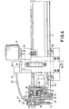
- Figures 1 and 2 are a side elevation and a plan view, respectively, of one feasible embodiment of a device for placing components on a substrate.
- the reference numeral 1 in these Figures denotes a substrate, for example, a printed circuit board which has already been provided on its lower side with conventional components 2 whose lead-outs are positioned in holes in the substrate.
- On the upper side of the substrate there are to be provided a large number of further components which are very small and which do not comprise lead-outs.
- the dimensions of this kind of component which is also referred to as a"chip-type" component, are of the order of 2.3 x 1.6 mm. These components must be very accurately positioned on the substrate at a very small distance from one another.
- the substrate 1 is supported by a substrate carrier 3.
- the components to be placed on the substrate are packaged in tapes, the components being loosely arranged in cavities in the tape which are closed on one side by a lower foil and on the other side by a cover foil.
- a number of such tapes is wound on reels 4 in a holder 5.
- the holder 5 comprises on both sides a projecting plate 100 with a hole 101 which can co-operate with a pin 102 on a feed device 7. At the bottom the holder 5 bears against the feed device through two supports 103.
- the tapes 6 extend from the reels 4 to a device for feeding the tapes to a number of presentation positions 11 for the components.
- the components can be picked up in these positions by a transfer mechanism 8,
- the transfer mechanism 8 mainly comprises a carriage 9 which is movable in the X-direction and a pick-up device 10 which is movable relative to the carriage in the Y-direction.
- the pick-up device 10 also comprises a number of pick-up elements 12 which are constructed as suction tubes.
- the holder 5 and the feed device 7 may be constructed as described in detail in Netherlands Patent Application 81 03 573.
- the pick-up elements 12 are arranged in the pick-up device 10 in a pattern which corresponds to the pattern of the presentation positions 11. This means that when the pick-up device 10 has been moved to a position over the presentation positions by movement of the carriage 9, each of the pick-up elements is situated over a presentation position.
- the suction tubes 12 are then moved to contact the components and all the suction tubes simultaneously pick up a component.
- the pick-up device is moved to a position over an adhesive-applying device 13.
- This device comprises an adhesive container 14 and a number of reciprocable adhesive-applying members 15 which are arranged in the same pattern as the presentation positions and the pick-up elements. This construction enables the pick-up device, after picking up the components, to be displaced to a position over the adhesive-applying device so that adhesive can be simultaneously applied to all the components by raising the adhesive-applying members and/or lowering the suction tubes and with them the components.
- the pick-up device 10 is moved further in the X-direction until it is in a position over the substrate. This operation is followed by a process during which each of the pick-up elements 12 in succession is moved to a position over the position on the substrate at which the relevant component is to be deposited. Deposition of the component is performed by lowering the relevant suction tube and, when the component contacts the substrate, by interrupting the vacuum connection to the tube.
- suction tubes which are present at the same time over the appropriate position on the substrate can be operated simultaneously, so that a group of components can be placed on the substrate in a selected position of the pick-up device.
- the carriage 9 and the pick-up device 10 may each be driven by a separate motor; the motors can be controlled by a program.
- the program will preferably be designed so that the pick-up device always travels the shortest possible distance over the substrate.
- presentation positions 11 and the pick-up elements 12 are arranged in a straight line in the present embodiment, obviously other arrangements may alternatively be chosen.
- movements in both the X and Y directions are imparted to the pick-up device.
- the X-movement may be performed by the carriage 9 and the X-movement by the substrate, in which case, for example, the substrate support 3 must be displaceable on a suitable guide.
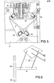
- Figure 3, 4 and 5 show the transfer mechanism 8 in a plan view, a part-sectional side elevation and a cross-section taken along the line V-V, respectively.
- the carriage 9 comprises a rack 22 which is engaged by a pinion 23.
- the pinion 23 is fixed on a shaft 24 which is journalled in the housing 21 and whose upper end carries a gearwheel 25 which meshes with a gearwheel 26 on the shaft of an electric motor 27.
- the carriage 9 can thus be moved to and fro in the housing 21 by means of the motor 27.
- the carriage 9 comprises at one end a transverse section 30 which comprises a number of guides 31.
- a transverse carriage 32 is co-operates with the guides 31 through a number of rollers 33.
- an electric motor 34 drives a rack 38 which forms part of the transverse carriage 32.
- a bar-shaped section 40 which supports a large number of suction tubes 41 (32 in this case) is coupled to the transverse carriage 32.
- the suction tubes may, for example, have a construction as described in Netherlands Patent Application 8201593 (PHN 10.325).
- Each of the suction tubes 41 can be moved downwards by compressed air, against the force of a spring, in order to be connected to a vacuum source in this position.
- the holder accommodating each of the suction tubes is provided at its upper end with a pinion 42 which meshes with a rack 43 which is connected to a section 44 which extends over the full length of the bar 40 and which can be moved to and fro between two positions by means of an air motor 45.
- the stroke of the section 44 is such that the suction tubes each perform a rotation of 180 during each stroke.
- Each of the suction tubes 41 communicates with an associated compressed air connection 46 and an associated vacuum connection 47.
- Each of these connections is connected, via a flexible pipe 50, to a valve block 51 which comprises controllable valves which open and close the relevant pipes at appropriate instants under the control of a program.
- valve block 51 can be simultaneously opened so that the suction tubes are lowered onto the chips which are subsequently picked up by the suction in the tubes.
- the bar 40 with the suction tubes 41 is moved to a position over the adhesine-applying device, so that adhesive is applied to the chips.
- the bar 40 with the suction tubes 41 is moved to a position over a substrate and the motors 27 and 34 are operated so that each of the suction tubes in succession is brought to a position over the position in which the relevant component is to be placed on the substrate.
- the relevant air valve When a suction tube has been positioned over the relevant position on the substrate, the relevant air valve is opened and the suction tube lowers the component onto the substrate, after which the suction is interrupted. Prior to the placing of the component on the substrate, the relevant suction tube may also be rotated through 180°.
- a substrate can thus be very quickly provided with components in accordance with a fixed program.
- Figure 6 shows how the suction tube bar 60 may also be connected to a bar 61 which is connected to a pantograph system 62.
- the bar 60 can thus again be placed in any desired position.
- the suction tubes are again controlled by means of compressed air and vacuum via an appropriate valve block whose valves are controlled in accordance with the position occupied by the bar 60.
- the bar 60 also comprises a pin 63 which is moved successively to positions over a given number of reference points in accordance with a given program.
Landscapes
- Engineering & Computer Science (AREA)
- Manufacturing & Machinery (AREA)
- Microelectronics & Electronic Packaging (AREA)
- Supply And Installment Of Electrical Components (AREA)
- Die Bonding (AREA)
Priority Applications (1)
| Application Number | Priority Date | Filing Date | Title |
|---|---|---|---|
| AT83200563T ATE19327T1 (de) | 1982-04-21 | 1983-04-19 | Verfahren und vorrichtung zum anordnen chipfoermiger elektrischer und/oder elektronischer komponenten auf einem substrat. |
Applications Claiming Priority (2)
| Application Number | Priority Date | Filing Date | Title |
|---|---|---|---|
| NL8201653 | 1982-04-21 | ||
| NL8201653A NL8201653A (nl) | 1982-04-21 | 1982-04-21 | Werkwijze en inrichting voor het plaatsen van chipvormige electrische en/of electronische onderdelen op een substraat. |
Publications (2)
| Publication Number | Publication Date |
|---|---|
| EP0092292A1 true EP0092292A1 (fr) | 1983-10-26 |
| EP0092292B1 EP0092292B1 (fr) | 1986-04-16 |
Family
ID=19839624
Family Applications (1)
| Application Number | Title | Priority Date | Filing Date |
|---|---|---|---|
| EP83200563A Expired EP0092292B1 (fr) | 1982-04-21 | 1983-04-19 | Procédure et dispositif à monter des composants électriques et/ou électroniques en forme de chip sur un substrat |
Country Status (9)
| Country | Link |
|---|---|
| US (1) | US4644642A (fr) |
| EP (1) | EP0092292B1 (fr) |
| JP (1) | JPS58191494A (fr) |
| KR (1) | KR910003146B1 (fr) |
| AT (1) | ATE19327T1 (fr) |
| CA (1) | CA1204528A (fr) |
| DE (1) | DE3363018D1 (fr) |
| HK (1) | HK85391A (fr) |
| NL (1) | NL8201653A (fr) |
Cited By (9)
| Publication number | Priority date | Publication date | Assignee | Title |
|---|---|---|---|---|
| US4465543A (en) * | 1981-09-22 | 1984-08-14 | Tokyo Shibaura Denki Kabushiki Kaisha | Apparatus and method for arranging semiconductor pellets |
| FR2560477A1 (fr) * | 1984-02-24 | 1985-08-30 | Pace Inc | Dispositif pour fixer a un support isolant des composants electroniques modulaires ou pour les retirer de ce dernier |
| EP0183301A1 (fr) * | 1984-11-19 | 1986-06-04 | Koninklijke Philips Electronics N.V. | Dispositif pour poser des composants électroniques et/ou électriques sur un substrat |
| FR2575630A1 (fr) * | 1984-09-17 | 1986-07-04 | Tdk Corp | Procede de montage d'elements de circuit du type puce sur des plaquettes de circuit imprime et appareil associe |
| EP0190372A1 (fr) * | 1985-01-29 | 1986-08-13 | TEKMA KINOMAT S.p.A. | Procédé pour le positionnement automatique de puces sur des circuits imprimés et machine pour sa mise en oeuvre |
| EP0377248A1 (fr) * | 1989-01-06 | 1990-07-11 | Koninklijke Philips Electronics N.V. | Procédé et dispositif pour placer des composants sur un support |
| EP0434156A1 (fr) * | 1989-12-21 | 1991-06-26 | Koninklijke Philips Electronics N.V. | Dispositif comprenant au moins deux manipulateurs, un dispositif de positionnement pour le placement de composants électriques sur un support et un dispositif de préhension à utiliser dans un tel dispositif de positionnement |
| US5216804A (en) * | 1991-05-21 | 1993-06-08 | U.S. Philips Corp. | Method and device for placing a component on a printed circuit board |
| NL9302155A (nl) * | 1993-12-10 | 1995-07-03 | Boschman Holding Bv | Inrichting voor het in vormholten plaatsen van voorwerpen. |
Families Citing this family (11)
| Publication number | Priority date | Publication date | Assignee | Title |
|---|---|---|---|---|
| JPS60242922A (ja) * | 1984-05-18 | 1985-12-02 | Tokico Ltd | 部品取付け装置 |
| JPS6171693A (ja) * | 1984-09-17 | 1986-04-12 | ティーディーケイ株式会社 | チツプ部品の装着方法 |
| NL8701139A (nl) * | 1987-05-13 | 1988-12-01 | Philips Nv | Geleideinrichting. |
| CA1320005C (fr) * | 1988-06-16 | 1993-07-06 | Kotaro Harigane | Dispositif de montage d'element electronique |
| JPH0250440A (ja) * | 1988-08-12 | 1990-02-20 | Mitsubishi Electric Corp | ダイボンド装置 |
| JP2526602Y2 (ja) * | 1988-10-18 | 1997-02-19 | 山形カシオ 株式会社 | 電子部品自動取上げ装置 |
| JPH0268499U (fr) * | 1988-11-11 | 1990-05-24 | ||
| JP4346174B2 (ja) * | 1998-10-13 | 2009-10-21 | パナソニック株式会社 | 電子部品実装装置 |
| KR100348400B1 (ko) * | 2000-05-20 | 2002-08-10 | 미래산업 주식회사 | 표면실장장치의 모듈헤드의 노즐회전장치 |
| DE102005033979B4 (de) * | 2005-07-20 | 2007-08-02 | Siemens Ag | Bestücksystem und Verfahren zum Bestücken von Substraten mit elektrischen Bauteilen |
| JP5302773B2 (ja) * | 2009-05-27 | 2013-10-02 | 株式会社日立ハイテクノロジーズ | 電子部品実装装置 |
Citations (4)
| Publication number | Priority date | Publication date | Assignee | Title |
|---|---|---|---|---|
| US4166562A (en) * | 1977-09-01 | 1979-09-04 | The Jade Corporation | Assembly system for microcomponent devices such as semiconductor devices |
| EP0013979A1 (fr) * | 1979-01-25 | 1980-08-06 | Matsushita Electric Industrial Co., Ltd. | Appareil pour monter des parties électroniques |
| EP0016368A1 (fr) * | 1979-03-05 | 1980-10-01 | Matsushita Electric Industrial Co., Ltd. | Dispositif pour la fixation de composants |
| DE2923695A1 (de) * | 1979-06-12 | 1980-12-18 | Ruf Kg Wilhelm | Vorrichtung zur aufnahme und positionsgerechten ablage von bauteilen |
Family Cites Families (21)
| Publication number | Priority date | Publication date | Assignee | Title |
|---|---|---|---|---|
| US3611561A (en) * | 1969-04-21 | 1971-10-12 | Paul A Dosier | Transfer mechanism with loading nest |
| US3859723A (en) * | 1973-11-05 | 1975-01-14 | Microsystems Int Ltd | Bonding method for multiple chip arrays |
| US3958740A (en) * | 1974-07-08 | 1976-05-25 | Dixon Automation, Inc. | Automatic component assembly machine and method relating thereto |
| JPS51131273A (en) * | 1975-05-10 | 1976-11-15 | Fujitsu Ltd | Wire bonding process |
| JPS51131274A (en) * | 1975-05-10 | 1976-11-15 | Fujitsu Ltd | Tip bonding method |
| JPS52124168A (en) * | 1976-04-12 | 1977-10-18 | Matsushita Electric Industrial Co Ltd | Method of assembling electronic device circuit |
| FR2365209A1 (fr) * | 1976-09-20 | 1978-04-14 | Cii Honeywell Bull | Procede pour le montage de micro-plaquettes de circuits integres sur un substrat et installation pour sa mise en oeuvre |
| US4151945A (en) * | 1977-12-08 | 1979-05-01 | Universal Instruments Corporation | Automated hybrid circuit board assembly apparatus |
| US4292116A (en) * | 1978-04-18 | 1981-09-29 | Tokyo Denki Kagaku Kogyo Kabushiki Kaisha | Apparatus for mounting chip type circuit elements on a printed circuit board |
| JPS5537283A (en) * | 1978-09-08 | 1980-03-15 | Matsushita Electric Industrial Co Ltd | Article shifter |
| JPS5921200B2 (ja) * | 1978-10-24 | 1984-05-18 | 日本電気ホームエレクトロニクス株式会社 | 部品同時配列供給装置 |
| GB2034613B (en) * | 1978-11-09 | 1983-01-19 | Tokyo Shibaura Electric Co | Method and apparatus for mounting electronic components |
| JPS5583239A (en) * | 1978-12-20 | 1980-06-23 | Hitachi Ltd | Mounting tip element |
| JPS55118690A (en) * | 1979-03-05 | 1980-09-11 | Matsushita Electric Industrial Co Ltd | Device for carrying electronic part |
| US4345371A (en) * | 1979-03-14 | 1982-08-24 | Sony Corporation | Method and apparatus for manufacturing hybrid integrated circuits |
| DE2935081C2 (de) * | 1979-08-30 | 1985-12-19 | Philips Patentverwaltung Gmbh, 2000 Hamburg | Vorrichtung zur Bestückung von Leiterplatten. |
| JPS5636196A (en) * | 1979-09-03 | 1981-04-09 | Sony Corp | Apparatus for assembling electronic device circuit |
| JPS5661194A (en) * | 1979-10-25 | 1981-05-26 | Hitachi Ltd | Method of carrying chip element |
| JPS6311756Y2 (fr) * | 1980-04-25 | 1988-04-05 | ||
| JPS576277U (fr) * | 1980-06-12 | 1982-01-13 | ||
| JPS5737281U (fr) * | 1980-08-13 | 1982-02-27 |
-
1982
- 1982-04-21 NL NL8201653A patent/NL8201653A/nl not_active Application Discontinuation
-
1983
- 1983-04-13 CA CA000425753A patent/CA1204528A/fr not_active Expired
- 1983-04-19 AT AT83200563T patent/ATE19327T1/de not_active IP Right Cessation
- 1983-04-19 EP EP83200563A patent/EP0092292B1/fr not_active Expired
- 1983-04-19 DE DE8383200563T patent/DE3363018D1/de not_active Expired
- 1983-04-20 JP JP58068492A patent/JPS58191494A/ja active Pending
- 1983-04-20 KR KR1019830001670A patent/KR910003146B1/ko not_active Expired
-
1985
- 1985-09-03 US US06/772,196 patent/US4644642A/en not_active Expired - Fee Related
-
1991
- 1991-10-31 HK HK853/91A patent/HK85391A/xx unknown
Patent Citations (4)
| Publication number | Priority date | Publication date | Assignee | Title |
|---|---|---|---|---|
| US4166562A (en) * | 1977-09-01 | 1979-09-04 | The Jade Corporation | Assembly system for microcomponent devices such as semiconductor devices |
| EP0013979A1 (fr) * | 1979-01-25 | 1980-08-06 | Matsushita Electric Industrial Co., Ltd. | Appareil pour monter des parties électroniques |
| EP0016368A1 (fr) * | 1979-03-05 | 1980-10-01 | Matsushita Electric Industrial Co., Ltd. | Dispositif pour la fixation de composants |
| DE2923695A1 (de) * | 1979-06-12 | 1980-12-18 | Ruf Kg Wilhelm | Vorrichtung zur aufnahme und positionsgerechten ablage von bauteilen |
Cited By (9)
| Publication number | Priority date | Publication date | Assignee | Title |
|---|---|---|---|---|
| US4465543A (en) * | 1981-09-22 | 1984-08-14 | Tokyo Shibaura Denki Kabushiki Kaisha | Apparatus and method for arranging semiconductor pellets |
| FR2560477A1 (fr) * | 1984-02-24 | 1985-08-30 | Pace Inc | Dispositif pour fixer a un support isolant des composants electroniques modulaires ou pour les retirer de ce dernier |
| FR2575630A1 (fr) * | 1984-09-17 | 1986-07-04 | Tdk Corp | Procede de montage d'elements de circuit du type puce sur des plaquettes de circuit imprime et appareil associe |
| EP0183301A1 (fr) * | 1984-11-19 | 1986-06-04 | Koninklijke Philips Electronics N.V. | Dispositif pour poser des composants électroniques et/ou électriques sur un substrat |
| EP0190372A1 (fr) * | 1985-01-29 | 1986-08-13 | TEKMA KINOMAT S.p.A. | Procédé pour le positionnement automatique de puces sur des circuits imprimés et machine pour sa mise en oeuvre |
| EP0377248A1 (fr) * | 1989-01-06 | 1990-07-11 | Koninklijke Philips Electronics N.V. | Procédé et dispositif pour placer des composants sur un support |
| EP0434156A1 (fr) * | 1989-12-21 | 1991-06-26 | Koninklijke Philips Electronics N.V. | Dispositif comprenant au moins deux manipulateurs, un dispositif de positionnement pour le placement de composants électriques sur un support et un dispositif de préhension à utiliser dans un tel dispositif de positionnement |
| US5216804A (en) * | 1991-05-21 | 1993-06-08 | U.S. Philips Corp. | Method and device for placing a component on a printed circuit board |
| NL9302155A (nl) * | 1993-12-10 | 1995-07-03 | Boschman Holding Bv | Inrichting voor het in vormholten plaatsen van voorwerpen. |
Also Published As
| Publication number | Publication date |
|---|---|
| EP0092292B1 (fr) | 1986-04-16 |
| KR840004829A (ko) | 1984-10-24 |
| KR910003146B1 (ko) | 1991-05-20 |
| ATE19327T1 (de) | 1986-05-15 |
| HK85391A (en) | 1991-11-08 |
| NL8201653A (nl) | 1983-11-16 |
| US4644642A (en) | 1987-02-24 |
| CA1204528A (fr) | 1986-05-13 |
| DE3363018D1 (en) | 1986-05-22 |
| JPS58191494A (ja) | 1983-11-08 |
Similar Documents
| Publication | Publication Date | Title |
|---|---|---|
| EP0092292B1 (fr) | Procédure et dispositif à monter des composants électriques et/ou électroniques en forme de chip sur un substrat | |
| CA1238985A (fr) | Methode et appareil de manutention de pieces electriques | |
| US5040291A (en) | Multi-spindle pick and place method and apparatus | |
| EP0071302A1 (fr) | Procédé et dispositif pour dispenser des composants électriques et/ou électroniques dans des positions données | |
| US6691400B1 (en) | High speed electronic parts mounting apparatus having mounting heads which alternately mount components on a printed circuit board | |
| WO1997020455A1 (fr) | Dispositif et procede de montage de composants electroniques | |
| KR100400106B1 (ko) | 멀티칩 본딩 방법 및 장치 | |
| US6811370B2 (en) | Wafer handling robot having X-Y stage for wafer handling and positioning | |
| JPH0322076B2 (fr) | ||
| CN100449718C (zh) | 用于安装半导体芯片的方法和装置 | |
| JPH06166428A (ja) | ワーク移載装置 | |
| EP0194739B1 (fr) | Procédé et dispositif de positionnement précis d'un composant solide pour le prélèvement par robot | |
| US4671722A (en) | Automatic positioning of electronic components on a walking beam | |
| US6397456B1 (en) | Method and a machine for automatic mounting of components and a pick-up head for such a machine | |
| JP3114427B2 (ja) | 電子部品供給装置および電子部品供給方法 | |
| JPH0247118B2 (fr) | ||
| JPS62285843A (ja) | 基板形部品授受装置 | |
| EP1051893B1 (fr) | Appareil de placement de composants | |
| JP3301433B2 (ja) | 電子部品実装装置 | |
| KR20010025827A (ko) | 표면실장장치 및 그 실장방법 | |
| JP3339499B2 (ja) | 電子部品実装方法 | |
| JPH0897595A (ja) | 電子部品実装装置 | |
| CN100461999C (zh) | 用于提供电气组件的晶片工作台和用于为基底配备电气组件的装置 | |
| EP4243060A1 (fr) | Appareil et procédé de fourniture de tranches pour machine d'assemblage automatique, et système d'assemblage | |
| CN121929531A (zh) | Fpc的钢片阻值测试设备及fpc生产线 |
Legal Events
| Date | Code | Title | Description |
|---|---|---|---|
| PUAI | Public reference made under article 153(3) epc to a published international application that has entered the european phase |
Free format text: ORIGINAL CODE: 0009012 |
|
| AK | Designated contracting states |
Designated state(s): AT CH DE FR GB IT LI NL |
|
| 17P | Request for examination filed |
Effective date: 19831201 |
|
| GRAA | (expected) grant |
Free format text: ORIGINAL CODE: 0009210 |
|
| AK | Designated contracting states |
Kind code of ref document: B1 Designated state(s): AT CH DE FR GB IT LI NL |
|
| REF | Corresponds to: |
Ref document number: 19327 Country of ref document: AT Date of ref document: 19860515 Kind code of ref document: T |
|
| REF | Corresponds to: |
Ref document number: 3363018 Country of ref document: DE Date of ref document: 19860522 |
|
| ITF | It: translation for a ep patent filed | ||
| ET | Fr: translation filed | ||
| PLBE | No opposition filed within time limit |
Free format text: ORIGINAL CODE: 0009261 |
|
| STAA | Information on the status of an ep patent application or granted ep patent |
Free format text: STATUS: NO OPPOSITION FILED WITHIN TIME LIMIT |
|
| 26N | No opposition filed | ||
| PGFP | Annual fee paid to national office [announced via postgrant information from national office to epo] |
Ref country code: AT Payment date: 19900423 Year of fee payment: 8 |
|
| PGFP | Annual fee paid to national office [announced via postgrant information from national office to epo] |
Ref country code: NL Payment date: 19900430 Year of fee payment: 8 |
|
| PG25 | Lapsed in a contracting state [announced via postgrant information from national office to epo] |
Ref country code: AT Effective date: 19910419 |
|
| PG25 | Lapsed in a contracting state [announced via postgrant information from national office to epo] |
Ref country code: NL Effective date: 19911101 |
|
| NLV4 | Nl: lapsed or anulled due to non-payment of the annual fee | ||
| PGFP | Annual fee paid to national office [announced via postgrant information from national office to epo] |
Ref country code: GB Payment date: 19930401 Year of fee payment: 11 |
|
| PGFP | Annual fee paid to national office [announced via postgrant information from national office to epo] |
Ref country code: FR Payment date: 19930428 Year of fee payment: 11 |
|
| ITTA | It: last paid annual fee | ||
| PGFP | Annual fee paid to national office [announced via postgrant information from national office to epo] |
Ref country code: DE Payment date: 19930628 Year of fee payment: 11 |
|
| PGFP | Annual fee paid to national office [announced via postgrant information from national office to epo] |
Ref country code: CH Payment date: 19930720 Year of fee payment: 11 |
|
| PG25 | Lapsed in a contracting state [announced via postgrant information from national office to epo] |
Ref country code: GB Effective date: 19940419 |
|
| PG25 | Lapsed in a contracting state [announced via postgrant information from national office to epo] |
Ref country code: LI Effective date: 19940430 Ref country code: CH Effective date: 19940430 |
|
| GBPC | Gb: european patent ceased through non-payment of renewal fee |
Effective date: 19940419 |
|
| PG25 | Lapsed in a contracting state [announced via postgrant information from national office to epo] |
Ref country code: FR Effective date: 19941229 |
|
| REG | Reference to a national code |
Ref country code: CH Ref legal event code: PL |
|
| PG25 | Lapsed in a contracting state [announced via postgrant information from national office to epo] |
Ref country code: DE Effective date: 19950103 |
|
| REG | Reference to a national code |
Ref country code: FR Ref legal event code: ST |