EP0092412A2 - Vorrichtung zur Aussendung von Super-Fluoreszenzlicht - Google Patents
Vorrichtung zur Aussendung von Super-Fluoreszenzlicht Download PDFInfo
- Publication number
- EP0092412A2 EP0092412A2 EP83302174A EP83302174A EP0092412A2 EP 0092412 A2 EP0092412 A2 EP 0092412A2 EP 83302174 A EP83302174 A EP 83302174A EP 83302174 A EP83302174 A EP 83302174A EP 0092412 A2 EP0092412 A2 EP 0092412A2
- Authority
- EP
- European Patent Office
- Prior art keywords
- material layers
- pumping
- ray
- atoms
- rays
- Prior art date
- Legal status (The legal status is an assumption and is not a legal conclusion. Google has not performed a legal analysis and makes no representation as to the accuracy of the status listed.)
- Withdrawn
Links
- 239000000463 material Substances 0.000 claims abstract description 71
- 238000005086 pumping Methods 0.000 claims abstract description 41
- 230000002269 spontaneous effect Effects 0.000 claims abstract description 4
- 230000007704 transition Effects 0.000 claims description 13
- 239000011521 glass Substances 0.000 claims description 10
- 230000005284 excitation Effects 0.000 claims description 7
- 230000001678 irradiating effect Effects 0.000 claims description 4
- 229910021570 Manganese(II) fluoride Inorganic materials 0.000 claims description 3
- CTNMMTCXUUFYAP-UHFFFAOYSA-L difluoromanganese Chemical compound F[Mn]F CTNMMTCXUUFYAP-UHFFFAOYSA-L 0.000 claims description 3
- 229910001635 magnesium fluoride Inorganic materials 0.000 claims description 3
- 229910052759 nickel Inorganic materials 0.000 claims description 3
- 229910052710 silicon Inorganic materials 0.000 claims description 3
- 150000001875 compounds Chemical class 0.000 claims 2
- 229910004613 CdTe Inorganic materials 0.000 claims 1
- 229910000673 Indium arsenide Inorganic materials 0.000 claims 1
- 229910007709 ZnTe Inorganic materials 0.000 claims 1
- WPYVAWXEWQSOGY-UHFFFAOYSA-N indium antimonide Chemical compound [Sb]#[In] WPYVAWXEWQSOGY-UHFFFAOYSA-N 0.000 claims 1
- RPQDHPTXJYYUPQ-UHFFFAOYSA-N indium arsenide Chemical compound [In]#[As] RPQDHPTXJYYUPQ-UHFFFAOYSA-N 0.000 claims 1
- 230000001427 coherent effect Effects 0.000 abstract description 20
- 230000010356 wave oscillation Effects 0.000 abstract description 2
- 239000010410 layer Substances 0.000 description 66
- 238000010894 electron beam technology Methods 0.000 description 11
- 238000009826 distribution Methods 0.000 description 10
- 238000010586 diagram Methods 0.000 description 9
- 230000010355 oscillation Effects 0.000 description 8
- 230000005855 radiation Effects 0.000 description 7
- 239000007787 solid Substances 0.000 description 7
- 230000008859 change Effects 0.000 description 5
- 150000002500 ions Chemical class 0.000 description 5
- 230000003993 interaction Effects 0.000 description 4
- 230000005283 ground state Effects 0.000 description 3
- 229910052725 zinc Inorganic materials 0.000 description 3
- XKRFYHLGVUSROY-UHFFFAOYSA-N Argon Chemical compound [Ar] XKRFYHLGVUSROY-UHFFFAOYSA-N 0.000 description 2
- VYPSYNLAJGMNEJ-UHFFFAOYSA-N Silicium dioxide Chemical compound O=[Si]=O VYPSYNLAJGMNEJ-UHFFFAOYSA-N 0.000 description 2
- 238000010521 absorption reaction Methods 0.000 description 2
- 230000002596 correlated effect Effects 0.000 description 2
- 230000000694 effects Effects 0.000 description 2
- 239000007789 gas Substances 0.000 description 2
- 239000011229 interlayer Substances 0.000 description 2
- 238000004519 manufacturing process Methods 0.000 description 2
- 230000007246 mechanism Effects 0.000 description 2
- 238000000034 method Methods 0.000 description 2
- 230000000737 periodic effect Effects 0.000 description 2
- 239000000758 substrate Substances 0.000 description 2
- 229910001218 Gallium arsenide Inorganic materials 0.000 description 1
- XUIMIQQOPSSXEZ-UHFFFAOYSA-N Silicon Chemical compound [Si] XUIMIQQOPSSXEZ-UHFFFAOYSA-N 0.000 description 1
- 230000009471 action Effects 0.000 description 1
- 229910052786 argon Inorganic materials 0.000 description 1
- 239000003990 capacitor Substances 0.000 description 1
- 239000002826 coolant Substances 0.000 description 1
- 238000001816 cooling Methods 0.000 description 1
- 230000000875 corresponding effect Effects 0.000 description 1
- 239000013078 crystal Substances 0.000 description 1
- 238000013016 damping Methods 0.000 description 1
- 230000007423 decrease Effects 0.000 description 1
- 238000005516 engineering process Methods 0.000 description 1
- 230000005281 excited state Effects 0.000 description 1
- 230000002349 favourable effect Effects 0.000 description 1
- 230000004927 fusion Effects 0.000 description 1
- CPBQJMYROZQQJC-UHFFFAOYSA-N helium neon Chemical compound [He].[Ne] CPBQJMYROZQQJC-UHFFFAOYSA-N 0.000 description 1
- 238000003475 lamination Methods 0.000 description 1
- 239000007788 liquid Substances 0.000 description 1
- 238000002844 melting Methods 0.000 description 1
- 230000008018 melting Effects 0.000 description 1
- 239000013307 optical fiber Substances 0.000 description 1
- 239000012466 permeate Substances 0.000 description 1
- 230000004044 response Effects 0.000 description 1
- 239000010979 ruby Substances 0.000 description 1
- 229910001750 ruby Inorganic materials 0.000 description 1
- 238000012216 screening Methods 0.000 description 1
- 230000035945 sensitivity Effects 0.000 description 1
- 239000010703 silicon Substances 0.000 description 1
- 239000012780 transparent material Substances 0.000 description 1
- 238000007738 vacuum evaporation Methods 0.000 description 1
Images




Classifications
-
- H—ELECTRICITY
- H01—ELECTRIC ELEMENTS
- H01S—DEVICES USING THE PROCESS OF LIGHT AMPLIFICATION BY STIMULATED EMISSION OF RADIATION [LASER] TO AMPLIFY OR GENERATE LIGHT; DEVICES USING STIMULATED EMISSION OF ELECTROMAGNETIC RADIATION IN WAVE RANGES OTHER THAN OPTICAL
- H01S3/00—Lasers, i.e. devices using stimulated emission of electromagnetic radiation in the infrared, visible or ultraviolet wave range
- H01S3/09—Processes or apparatus for excitation, e.g. pumping
- H01S3/091—Processes or apparatus for excitation, e.g. pumping using optical pumping
- H01S3/0915—Processes or apparatus for excitation, e.g. pumping using optical pumping by incoherent light
- H01S3/09155—Processes or apparatus for excitation, e.g. pumping using optical pumping by incoherent light by cathodo-luminescence
-
- H—ELECTRICITY
- H01—ELECTRIC ELEMENTS
- H01S—DEVICES USING THE PROCESS OF LIGHT AMPLIFICATION BY STIMULATED EMISSION OF RADIATION [LASER] TO AMPLIFY OR GENERATE LIGHT; DEVICES USING STIMULATED EMISSION OF ELECTROMAGNETIC RADIATION IN WAVE RANGES OTHER THAN OPTICAL
- H01S4/00—Devices using stimulated emission of electromagnetic radiation in wave ranges other than those covered by groups H01S1/00, H01S3/00 or H01S5/00, e.g. phonon masers, X-ray lasers or gamma-ray lasers
Definitions
- the present invention relates to a lighting device which emits super fluorescent light.
- this lighting device shall be tentatively named “Solid Fluoter” (Solid State Super Fluorescent Lighting Device).
- Super fluorescent phenomena are interpreted as follows. Certain atoms are excited by pumping with a high energy photon beam, and the resulting atomic level electrons are emitted spontaneously. At this time, photons appear, and they correlate the nearest atoms with each other. The electric dipole moments of the affected atoms interfere simultaneously as a whole, to cause population inversion. In consequence, a coherent photon wave is emitted from a device.
- Coherent super fluorescent light has hitherto been observed when passing a high power laser beam through a gas plasma in pulsing fashion.
- the present invention is therefore directed to producing coherent super fluorescent light beams by means of solid state devices.
- Such beams may range from the X-ray region to the visible region.
- the inventor proposes a device with one dimensional pseudo reflection layer plate series which is able to emit photon pulses with coherent phase, and has a type of quantum standing photon wave oscillation in between the layer plates, by pumping with high energy exciting photons.
- the invention provides a device for emitting light comprising a structure in which first material layers emitting a predetermined electromagnetic wave when irradiated with a pumping ray or beam, are stacked with second material layers substantially transmitting the electromagnetic wave, and means for irradiating said structure with the pumping ray or beam, the time taken for the electromagnetic wave to pass between said second material layers being set smaller than a time constant of spontaneous emission in atoms of said first material layers.
- the mechanism which allows the emission of an X-ray coherent photon wave pulse is thought to be due to breaching of a dielectric reflection wall formed by the periodic layer plate and release of the standing wave of fluorescence photons in between adjacent walls, as a coherent wave pulse.
- the quantum standing wave of fluorescent photons due to pumping of high power exciting photons is formed at a periodic number from the ground state to higher states corresponding to the length between adjacent walls with dielectric constant due to correlation of dipole vector doped atoms with fluorescent field, and the coherency of the interference wave follows Young's rule for the timing of emission of fluorescence photon from atom dipole change of the nearest wall, caused by a high energy pumping photon wave.
- the walls are breached by increase of pumping photon number due to the increase of the real part of the dielectric constant in the wall, which causes the evolution of an X-ray coherent pulse.
- the mechanism for quantum standing wave in between walls is the same as for X-rays.
- the preferred structure of the present invention emits an electromagnetic wave such as fluorescence X-rays from fluorescent material layers arranged in a basic transparent material and which establishes the condition that a time (llc) in which the emitted light passes through the interspace (l) between the fluorescent material layers is not greater than a changing time (transition time: ⁇ R ) of an electron transition moment, namely, ⁇ R ⁇ l/c.
- ⁇ R transition time
- Figure la is a sectional view showing a typical example of a layered fluorescent atom wall structure in the basic solid for emitting a coherent photon wave by pumping (hereinbelow, also termed "layered structure with fluorescent wall plates periodically arranged”), while Figure lb is a typical perspective view of the layered structure.
- the oscillation frequency 0 of the group is the frequency of the photons for K ⁇ K c .
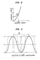
- Figure 3 shows a waveform indicative of the dipole variation +1 to -1 of the atoms, and the condition of the correlation between the photon wave and the dipole becomes:
- r denotes the interval of the atoms
- ⁇ S the time constant of the natural emission. Due to the pumping light (X-ray), the electron distribution undergoes population inversion. Then, the following holds:
- K K ⁇ K c
- lone excitation case for the inversion case K ⁇ K c
- N 2 and N 1 denote the high level electron density and low level density for the level transition of the atoms, respectively, the following holds in the stationary state:
- N 1 and N 2 become: and an electron distribution as shown in Figure 5 is established.
- the least number of photons of the standing wave fulfills, in a certain half wavelength region, the following conditions:
- This wave is very stable. It causes the dressed field at the correlated level of the atom group based on the superposition of the ground states. The lifetime is long, and the output of the evolved wave is of great power.
- the layered structure with the fluorescent wall plates periodically arranged is externally irradiated with, e. g., an electron beam 9 as pumping light in a direction parallel to the planes of fluorescent material layers 2 and support members 1.
- the electron beam is projected on a layer of Zn, Mn or the like (hereinbelow, tentatively named "radiant layer for pumping"), to generate high energy X-rays for excitation.
- the X-rays are used as pumping light for the fluorescent material layers 2.
- the energy of the pumping X-rays needs to be set at a level at which the X-rays can penetrate through the supporting layer 1 and can pump the fluorescent material so as to radiate fluorescent X-rays. That is, letting E ex denote the energy of the pumping light, the relationship among E , E f and E ex is so selected as to be E ex > E f > E s .
- E f denotes the energy of the radiant fluorescence
- E s the excitation energy for atomic level of the material of the supporting layer.
- the pumping light need not always be obtained by irradiating Zn or the like with the electron beam.
- the energies of the pumping light etc. satisfy the aforementioned condition, it is of course possible to directly use, e. g., a laser beam, X-ray beam or electron beam as the pumping light. Concrete examples will be described in detail in embodiments later.
- the thickness of the fluorescent material layer is preferably chosen so as to minimize the change of the phase difference of radiation within this layer.
- a transparent glass layer is set at a thickness of 10 4 ⁇ , which is approximately 10 times greater than an emission wavelength nearly equal to 1000 ⁇ .
- a thickness of, at o least, about 4000 A will be necessary for this layer.
- the thickness of the supporting layer 1 is so set that the arrival time of the radiation l/C) becomes smaller than the transition time ( ⁇ R ) of the levels of fluorescent material atoms. This is to be understood from the principle of the present invention stated before. Regarding the minimum thickness, the supporting layer may well be a monatomic layer as long as the function thereof is effected.
- fluorescent material layers are usable up to about 100 layers, they are ordinarily used up to about 20 layers.
- the length of the wall plate structure 10 in the direction of incidence of the pumping light is such that stable photon emission can be caused. This length is not a very important factor in the present device, Solid Fluoter, and a very great length is meaningless.
- the energy of X-ray photons 10 produced from the fluorescent material layer 1 under the aforementioned conditions affect the transition moments of the atoms of the adjacent fluorescent material layers in succession as typically illustrated in Figure 2.
- the situation is as exemplified below.
- Numeral 11 in Figure la denotes the X-rays which the radiant layer for pumping has generated when irradiated with the pumping light 9:
- the X-rays 11 reach the fluorescent material layer 2, and generate the fluorescence X-rays 10 in, e. g., a place 12. Owing to these fluorescence X-rays 10, the fluorescent material layer 2 generates the fluorescence X-rays 10 in, e..g., a place 13.
- the pumping radiant layer is not illustrated, an example thereof is as shown in Figure 11.
- the transition moments of the atoms affect one another, the time constant of the transition distribution of the natural emission of the individual atoms changes, and the electrons of all the atoms at the atomic levels are unified into the state of population inversion reverse to the Boltzmann distribution. Accordingly, the natural emission of the individual atoms tunes all the atoms so as to cause super fluorescent light of high power in the state of coherence.
- Ni is used as the material which produces the fluorescence X-rays
- Si as the supporting material which is transparent to the propagation of the X-rays
- Mo as the material which produces the exciting X-rays for pumping the fluorescent material
- a pulse electron flow of about 20 keV - 30 k eV of the order of picoseconds is emitted to the Mo material.
- exciting X-rays having a time constant smaller than where ⁇ p denotes the plasma oscillation frequency of the electromagnetic wave of the fluorescence X-rays of the Ni are produced from the Mo, to give rise to coherent X-rays in the spaces between the layers.
- the rate equation of the coherent X-rays is as has been explained with reference to Figures 4 to 8.
- the energies of the shells K, L, M etc. of the materials Si, Ni and Zn have values as indicated in Figure 9. Fine solid lines indicate the energies of the exciting X-rays, which pump to generate fluorescence X-rays in senses ⁇ . The energy difference between the K and L levels of the Si is great for the fluorescence X-rays, and this material is transparent with respect to the same.
- the axis of abscissas in Figure 9 represents the atomic number.
- the device of the present invention dispenses with a mirror for causing the feedback of light as in conventional laser devices.
- the output intensity (I) is expressed as follows: where f denotes the ratio of population inversion, N the number of photons, and I (k, 0) the natural output of one atom.
- the first term of the equation expressive of the output intensity indicates the spontaneous emission
- the second term the super fluorescence output of the square of the number N of photons resulting from the interaction between the atoms.
- the limitation at the lower energy end of the range is a result of the absorption of the radiation by the supporting material and the time constant of lattice vibration. More specifically, the lattice vibration of the supporting material is usually of 10 -12 - 10 -11 sec. The radiation has its energy absorbed and is scattered. Accordingly, the interaction between the atoms intended in the present invention fails to be accomplished.
- the emission is possible from the X-ray region to the infrared region.
- the interspace between the wall plates needs to be widened for the above reason, and difficulty is involved in the fabrication.
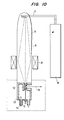
- FIG 10 is a model diagram showing the principle setup of a "Solid Fluoter” exemplifying the present invention.
- Numeral 6 designates an envelope, the interior of which is held at a vacuum of approximately 10 -8 Torr, in other words, as in ordinary vacuum tubes.
- a wall plate structure 10 is disposed at one end of the envelope 6. Naturally, this wall plate structure is so installed that a direction parallel to the planes of the fluorescent material layers and supporting material thereof agrees with the direction of incidence of pumping light.
- Numeral 7 indicates exciting means source which is, for example, an electron beam source. The distance between the exciting means source 7 and the wall plate structure 10 is set at about 30 cm.
- a focusing coil 8 is provided in order that the electron beam 9 from the electron beam source may be converged on the wall plate structure 10.
- exciting means other than an electron beam source such as an X -ray source or a laser device, may be used in conformity with the arrangement of the wall plate structure.
- a pulse current generated by a capacitor bank 16 is used as a power supply for the electron beam source, and the wall plate structure is irradiated with an electron flow of 20 keV - 30 keV.
- the wall plate structure is cooled in liquid air in order to prevent the wall plate from melting.
- Numeral 12 indicates an electrode which is connected to the wall plate structure, and numeral 13 cooling means. Arrows 14 indicate the stream of the coolant.
- the "Solid Fluoter" thus constructed can produce a super fluorescent light beam 15.
- FIG. 11 is a sectional view of a wall plate structure.
- fluorescent material layers 2 and supporting material layers 1 are alternately stacked.
- the fluorescent material was Ni, and its thickness was equivalent to a monatomic layer, while the supporting material was Si, and its thickness was controlled to 50 ⁇ .
- the fluorescent material layers 2 were stacked into 10 layers. The respective layers were formed by the well-known molecular-beam epitaxial growth method. Conventional vacuum evaporation may be resorted to for some thicknesses of the layers.
- a Zn or Mn plate 3 having a thickness of 10 ⁇ is mounted perpendicularly to the side surfaces of the respective layers of the lamination prepared as stated above.
- the wall plate structure thus constructed is set in frames 4 and 4' made of lead, as illustrated in the figure.
- Lead is favorable because it has the action of preventing X-rays from coming out.
- a window 5 for deriving a super fluorescent light beam is a circular opening having a diameter of 3 mm.
- This wall plate structure is installed on the envelope 6 as shown in Figure 10.
- Ni atoms are irradiated with X-rays having energy of 20 keV, and plasma oscillations arise in the layers in which the Ni atoms are contained.
- the theoretical intensity of coherent emission X-rays is evaluated by a rate equation.
- the quantum number of exciting X-rays is less than 5 % of the number of electrons.
- the electron flow is of 20 keV ⁇ 1 f sec, the pulsing coherent X-rays continue for 1 millisec and have photons in a number approximately equal to of the number of input electrons.
- Fluorescent material (CdS) layers 2 and supporting material (ZnS) layers 1 are alternately stacked on a ZnS substrate having an area of 10 mm x 10 mm
- the fluorescent material layer 2 was 5 ⁇ thick, and the supporting material layer 1 was 15.5 ⁇ m thick.
- the fluorescent material layers were stacked into 10 layers.
- the fluorescent material layers and the supporting material layers were formed by the molecular-beam epitaxial growth.
- the pumping radiant layer 3 is unnecessary unlike the case of Embodiment 1.
- a ruby laser as a pumping light source, a laser beam having a wavelength of 1.55 ⁇ m may be directly projected on the wall plate structure.
- the laser needs to have such an intensity that photons produced by the transition between energy levels in the Frenkel exciton cause plasma oscillations. An intensity of approximately 70 watts is used.
- the thickness of the supporting layer is set at about 1 ⁇ 2- 10 times of the emission wavelength.
- a wall plate structure can also be realized by employing a glass plate, MgF 2 , MnF 2 or the like for a supporting layer and forming the surface of the supporting layer with an Nd 3+ or Ni 2+ ion-containing layer as a fluorescent material layer.
- the surface of a quartz glass plate 16 having a diameter of 10 cm and a thickness of 10 4 A is diffused with Nd 3+ ions, to form an Nd 3+ layer 17.
- Nd is evaporated on the glass surface, whereupon the glass is heated to diffuse Nd thereinto.
- the density of the Nd ions is approximately 10 21 /m 3 .
- each glass plate is preferably set at (wavelength) x (1 - 10) or so.
- Ten glass plates 16 thus prepared are so stacked that the Nd +3 layers 17 and the bodies of the glass plates 16 are alternately arrayed, and they are mounted on frames 4 and 4' as in Figure 11.
- the pumping radiant layer 3 as in the embodiment of Figure 11 is unnecessary.
- Pumping light 18 is directly projected on the wall plate structure.
- the wall plate structure thus prepared is installed on the envelope 6 as shown in Figure 10. Using an argon laser (0.35 fm) or helium neon laser (0.63 ⁇ m) as a pumping light source, a super fluorescent light beam having an emission wavelength of 1.09 ⁇ m could be obtained.
- quartz glass is used for the glass plates
- glasses used for, e. g., optical fibers may be used as well.
- Glass-like plates of MgF 2 , MnF 2 etc. may be used as supporting members.
Landscapes
- Physics & Mathematics (AREA)
- Electromagnetism (AREA)
- Optics & Photonics (AREA)
- Engineering & Computer Science (AREA)
- Plasma & Fusion (AREA)
- Luminescent Compositions (AREA)
- Lasers (AREA)
- Apparatus For Radiation Diagnosis (AREA)
- X-Ray Techniques (AREA)
Applications Claiming Priority (2)
| Application Number | Priority Date | Filing Date | Title |
|---|---|---|---|
| JP63824/82 | 1982-04-19 | ||
| JP57063824A JPS58181000A (ja) | 1982-04-19 | 1982-04-19 | 同位相光超輻射発光装置 |
Publications (2)
| Publication Number | Publication Date |
|---|---|
| EP0092412A2 true EP0092412A2 (de) | 1983-10-26 |
| EP0092412A3 EP0092412A3 (de) | 1986-02-05 |
Family
ID=13240493
Family Applications (1)
| Application Number | Title | Priority Date | Filing Date |
|---|---|---|---|
| EP83302174A Withdrawn EP0092412A3 (de) | 1982-04-19 | 1983-04-18 | Vorrichtung zur Aussendung von Super-Fluoreszenzlicht |
Country Status (3)
| Country | Link |
|---|---|
| US (1) | US4791645A (de) |
| EP (1) | EP0092412A3 (de) |
| JP (1) | JPS58181000A (de) |
Cited By (1)
| Publication number | Priority date | Publication date | Assignee | Title |
|---|---|---|---|---|
| EP0191863A4 (de) * | 1984-07-30 | 1988-10-24 | Hitachi Ltd | Strahlengenerator. |
Families Citing this family (5)
| Publication number | Priority date | Publication date | Assignee | Title |
|---|---|---|---|---|
| US4938556A (en) * | 1983-11-25 | 1990-07-03 | The Board Of Trustees Of The Leland Stanford Junior University | Superfluorescent broadband fiber laser source |
| US5136600A (en) * | 1990-09-18 | 1992-08-04 | Litton Systems Inc. | Stabilization apparatus and method for an sfs |
| US5737354A (en) * | 1996-07-09 | 1998-04-07 | Sti Optronics, Inc. | Energy exchange between a laser beam and charged particles using inverse transition radiation and method for its use |
| US6552290B1 (en) * | 1999-02-08 | 2003-04-22 | Spectra Systems Corporation | Optically-based methods and apparatus for performing sorting coding and authentication using a gain medium that provides a narrowband emission |
| US7269190B2 (en) * | 2002-10-02 | 2007-09-11 | The Board Of Trustees Of The Leland Stanford Junior University | Er-doped superfluorescent fiber source with enhanced mean wavelength stability |
Family Cites Families (2)
| Publication number | Priority date | Publication date | Assignee | Title |
|---|---|---|---|---|
| US3338841A (en) * | 1964-05-14 | 1967-08-29 | Du Pont | Luminescent molybdate and tungstate compositions |
| US3760292A (en) * | 1970-12-22 | 1973-09-18 | Bell Telephone Labor Inc | Integrated feedback laser |
-
1982
- 1982-04-19 JP JP57063824A patent/JPS58181000A/ja active Pending
-
1983
- 1983-04-18 EP EP83302174A patent/EP0092412A3/de not_active Withdrawn
-
1986
- 1986-04-09 US US06/849,889 patent/US4791645A/en not_active Expired - Fee Related
Cited By (1)
| Publication number | Priority date | Publication date | Assignee | Title |
|---|---|---|---|---|
| EP0191863A4 (de) * | 1984-07-30 | 1988-10-24 | Hitachi Ltd | Strahlengenerator. |
Also Published As
| Publication number | Publication date |
|---|---|
| JPS58181000A (ja) | 1983-10-22 |
| EP0092412A3 (de) | 1986-02-05 |
| US4791645A (en) | 1988-12-13 |
Similar Documents
| Publication | Publication Date | Title |
|---|---|---|
| US3388314A (en) | Apparatus for generating radiation of frequencies higher than those of light | |
| Fetisov | X-ray diffraction methods for structural diagnostics of materials: progress and achievements | |
| US4704583A (en) | Light amplifiers employing collisions to produce a population inversion | |
| O'Sullivan et al. | Tunable narrowband soft x-ray source for projection lithography | |
| Baldacchini | Colored LiF: an optical material for all seasons | |
| EP0092412A2 (de) | Vorrichtung zur Aussendung von Super-Fluoreszenzlicht | |
| EP0802705A2 (de) | Verfahren und Vorrichtung zur Erzeugung von hochenergetischen kohärenten Elektronenstrahlen und Gammalaserstrahlen | |
| US4660203A (en) | Soft X-ray laser using pumping of 3P and 4P levels of He-like and H-like ions | |
| Cairns et al. | Using low and high prepulses to enhance the J= 0− 1 transition at 19.6 nm in the Ne-like germanium XUV laser | |
| Pellegrini et al. | The development of X-ray free-electron lasers | |
| KR20020052204A (ko) | 극자외선 소스를 얻는 방법, 광선의 소스 및 리소그라피공정에의 사용 | |
| US5117432A (en) | Vanadium-pumped titanium x-ray laser | |
| US4589113A (en) | Short wavelength laser | |
| Key | XUV lasers | |
| US20050030991A1 (en) | Dual layer color-center patterned light source | |
| Katsumi et al. | Microscopic studies of defect formation under dense electronic excitation in insulators | |
| Csonka | Insertion devices, future developments, limitations | |
| Delker et al. | Experimental verification of the relativistic fine-structure term of the Klein-Gordon equation in pionic titanium atoms | |
| Bressler et al. | Rydberg and charge transfer states of F atoms in neon matrices | |
| Bollanti et al. | Characteristics of a soft X-ray plasma source for different pumping laser configurations and spectral analysis | |
| Shtykov et al. | Some Types of Quantum Generators and Amplifiers | |
| Kaplin et al. | Intensive coherent X-rays from multilayer mirrors | |
| Fill et al. | X-ray laser research at the Max Planck Institute of Quantum Optics | |
| Yamanaka | Free electron laser: technical issues and prospects in Japan | |
| Matsuda et al. | Upgrading the RIKEN-RAL muon facility |
Legal Events
| Date | Code | Title | Description |
|---|---|---|---|
| PUAI | Public reference made under article 153(3) epc to a published international application that has entered the european phase |
Free format text: ORIGINAL CODE: 0009012 |
|
| 17P | Request for examination filed |
Effective date: 19830525 |
|
| AK | Designated contracting states |
Designated state(s): DE FR GB NL |
|
| PUAL | Search report despatched |
Free format text: ORIGINAL CODE: 0009013 |
|
| AK | Designated contracting states |
Designated state(s): DE FR GB NL |
|
| 17Q | First examination report despatched |
Effective date: 19870929 |
|
| STAA | Information on the status of an ep patent application or granted ep patent |
Free format text: STATUS: THE APPLICATION IS DEEMED TO BE WITHDRAWN |
|
| 18D | Application deemed to be withdrawn |
Effective date: 19890104 |
|
| RIN1 | Information on inventor provided before grant (corrected) |
Inventor name: KOMATSUBARA, KIICHI F. |