EP0094683A2 - Akustische Oberflächenwelleneinrichtung - Google Patents
Akustische Oberflächenwelleneinrichtung Download PDFInfo
- Publication number
- EP0094683A2 EP0094683A2 EP83104903A EP83104903A EP0094683A2 EP 0094683 A2 EP0094683 A2 EP 0094683A2 EP 83104903 A EP83104903 A EP 83104903A EP 83104903 A EP83104903 A EP 83104903A EP 0094683 A2 EP0094683 A2 EP 0094683A2
- Authority
- EP
- European Patent Office
- Prior art keywords
- surface acoustic
- acoustic wave
- output transducer
- transducer
- output
- Prior art date
- Legal status (The legal status is an assumption and is not a legal conclusion. Google has not performed a legal analysis and makes no representation as to the accuracy of the status listed.)
- Granted
Links
- 238000010897 surface acoustic wave method Methods 0.000 title claims abstract description 30
- 230000005236 sound signal Effects 0.000 claims abstract description 23
- 239000000758 substrate Substances 0.000 claims description 12
- 230000001143 conditioned effect Effects 0.000 claims description 3
- 230000008878 coupling Effects 0.000 description 2
- 238000010168 coupling process Methods 0.000 description 2
- 238000005859 coupling reaction Methods 0.000 description 2
- 210000005069 ears Anatomy 0.000 description 2
- 238000000926 separation method Methods 0.000 description 2
- 230000001629 suppression Effects 0.000 description 2
- 230000002411 adverse Effects 0.000 description 1
- XAGFODPZIPBFFR-UHFFFAOYSA-N aluminium Chemical compound [Al] XAGFODPZIPBFFR-UHFFFAOYSA-N 0.000 description 1
- 229910052782 aluminium Inorganic materials 0.000 description 1
- 230000005540 biological transmission Effects 0.000 description 1
- 239000002131 composite material Substances 0.000 description 1
- 239000013078 crystal Substances 0.000 description 1
- 230000003111 delayed effect Effects 0.000 description 1
- GQYHUHYESMUTHG-UHFFFAOYSA-N lithium niobate Chemical compound [Li+].[O-][Nb](=O)=O GQYHUHYESMUTHG-UHFFFAOYSA-N 0.000 description 1
- 238000004519 manufacturing process Methods 0.000 description 1
- 239000000463 material Substances 0.000 description 1
- 238000000034 method Methods 0.000 description 1
- 230000002265 prevention Effects 0.000 description 1
- 238000005549 size reduction Methods 0.000 description 1
Images
Classifications
-
- H—ELECTRICITY
- H03—ELECTRONIC CIRCUITRY
- H03H—IMPEDANCE NETWORKS, e.g. RESONANT CIRCUITS; RESONATORS
- H03H9/00—Networks comprising electromechanical or electro-acoustic elements; Electromechanical resonators
- H03H9/02—Details
- H03H9/125—Driving means, e.g. electrodes, coils
- H03H9/145—Driving means, e.g. electrodes, coils for networks using surface acoustic waves
- H03H9/14544—Transducers of particular shape or position
- H03H9/14552—Transducers of particular shape or position comprising split fingers
-
- H—ELECTRICITY
- H03—ELECTRONIC CIRCUITRY
- H03H—IMPEDANCE NETWORKS, e.g. RESONANT CIRCUITS; RESONATORS
- H03H9/00—Networks comprising electromechanical or electro-acoustic elements; Electromechanical resonators
- H03H9/02—Details
- H03H9/02535—Details of surface acoustic wave devices
- H03H9/02637—Details concerning reflective or coupling arrays
- H03H9/02779—Continuous surface reflective arrays
-
- H—ELECTRICITY
- H03—ELECTRONIC CIRCUITRY
- H03H—IMPEDANCE NETWORKS, e.g. RESONANT CIRCUITS; RESONATORS
- H03H9/00—Networks comprising electromechanical or electro-acoustic elements; Electromechanical resonators
- H03H9/70—Multiple-port networks for connecting several sources or loads, working on different frequencies or frequency bands, to a common load or source
- H03H9/72—Networks using surface acoustic waves
-
- H—ELECTRICITY
- H03—ELECTRONIC CIRCUITRY
- H03H—IMPEDANCE NETWORKS, e.g. RESONANT CIRCUITS; RESONATORS
- H03H9/00—Networks comprising electromechanical or electro-acoustic elements; Electromechanical resonators
- H03H9/02—Details
- H03H9/02535—Details of surface acoustic wave devices
- H03H9/02992—Details of bus bars, contact pads or other electrical connections for finger electrodes
Definitions
- This invention relates to a surface acoustic wave device for use in a television receiver set or the like.
- a surface acoustic wave filter adapted for separation of a tuner output into a picture channel and a sound channel, which filter comprises a piezoelectric substrate on which disposed are one input transducer connected to a tuner, and two output transducers for receiving surface acoustic waves and converting them into electrical signals.
- the-two output transducers are designed to have the same electrode aperture length probably because it is intended to make the impedance of one output transducer for sound signal identical with the impedance of the other output transducer for picture signal, the latter impedance being set for suppression of multipath reflection.
- the area of the substrate is approximately doubled as compared to that of a substrate carrying a single output transducer. Accordingly, this example of a composite surface acoustic wave filter inevitably requires a doubled quantity of substrate material, resulting in increase not only in production cost but also in the size of a packaged device, and can not be applicable to a packaged device conventionally used.
- Multipath reflective wave interfers with a main signal and is delivared out of the filter.
- To suppress such multipath reflective wave it is common practice to couple the filter to a succeeding amplifier in an impedance mismatching fashion.
- the impedance mismatching coupling can, for one thing, suppress the multipath reflection wave but for another thing, it will adversely attenuate the main signal.
- the suppression of multipath reflective wave can be accomplished only at the cost of the undesirable attenuation of the sound signal component.
- An object of the present invention is to provide a surface acoustic wave filter capable of transmitting sound signal without causing their attenuation.
- Another object of the present invention is to provide a surface acoustic wave filter capable of suppressing increase in the area of a filter substrate.
- multipath reflective wave is suppressed in a picture signal channel only, and an output transducer provided for a sound signal channel is so spaced apart from an input transducer that the delay time of the multipath reflective wave can be reduced to an extent that occurrence of the multipath reflective wave can not be discriminated and is conditioned to have a short electrode aperture length by making its output impedance high to thereby prevent attenuation of the sound signal due to impedance mismatching with a succeeding amplifier.
- TTE triple transit echo
- the TTE in a system for separation of a picture signal and a sound signal components, the TTE must be suppressed, like the conventional device, in the picture signal channel whereas the occurrence of the TTE in the sound signal channel is not serious if the delay time of the TTE is so short that human ears may be insensitive to the TTE. More particularly, when the period of comb like characteristics for the TTE as defined by a reciprocal of the delay time between disired signal and TTE is very large, amounting to, for example, 500 KHz of the TTE's interval for a sound signal of a band width of about 15 KHz, the frequency characteristics for the sound signal are not affected by the TTE comb like characteristics so that the sound signal can be substantially freed from distortion.
- the establishment of impedance matching between the output transducer and the succeeding amplifier is significantly effective for both the size reduction of the surface acoustic wave device and prevention of the signal attenuation.
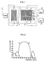
- a preferred embodiment of a surface acoustic wave device comprises an input transducer 1, a picture signal output transducer 2 and a sound signal output transducer 3.
- the input transducer 1 has 15 pairs of unapodized electrodes in which the finger width is 8.6 ⁇ m and the finger spacing and finger overlapping length are fixed, and its electrode aperture length is 2260 um.
- the picture signal output transducer 2 has 60 pairs of apodized electrodes in which the finger spacing and finger overlapping length are not uniform, and the sound signal output transducer 3 has 70 pairs of apodized electrodes in which the finger spacing and finger overlapping length are also not uniform.
- the output transducer 2 has an electrode aperture length W 2 of 1280 pm and the output transducer 3 has an electrode aperture length W 3 of 680 ⁇ m.
- the electrode finger of each transducer is of a double finger configuration (split type) and is made of 0 aluminum deposited films of 5000 A thickness formed by photolithographic technique on a surface of a piezo-electric substrate 8 made of a lithium niobate single crystal of 128° rotated Y-axis cut. Interposed between the input and output transducers is a shield electrode 4.
- the input transducer 1 cooperates with the output transducer 2 to provide frequency characteristics as shown in Fig. 2 wherein a self channel sound carrier fs, an upper adjacent picture carrier f p and a lower adjacent sound carrier fs are suppressed.
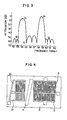
- the input transducer 1 is also in cooperation with the output transducer 3 to provide frequency characteristics as shown in Fig. 3 wherein other frequency components than the sound carrier fs and a picture carrier fp are suppressed.
- a picture signal component from the output transducer 2 is supplied to an amplifier 9, and a sound signal component and a picture carrier both delivered out of the output transducer 3 are supplied to an amplifier 10.
- Output signals of the amplifiers 9 and 10 are respectively subjected to necessary signal processing and then supplied to a picture tube and a loudspeaker, respectively.
- Each of the amplifiers 9 and 10 has an input impedance of about 300 0 and on the other hand, the output transducer 2 has an output impedance of about 150 ⁇ and the output transducer 3 has an output impedance of about 300 ⁇ . Therefore, while in the picture signal channel the TTE can be suppressed because of the impedance mismatching, a main signal and the TTE can not at all be suppressed in the sound signal channel where the impedance matching is completely established.
- the output transducer 3 is disposed in close proximity of the input transducer 1 so that the delay time of the TTE may be of the order of several micro seconds at the most and human ears may be completely insensitive to the interferring TTE.
- the transducer can be conditioned to assume a high impedance by reducing the electrical capacitance between paired fingers, and to this end, the duty factor defined by a ratio of finger width to structural period of interdigital electrodes can be reduced. For example, when the electrode aperture length is 980 ⁇ m, the finger width is 8.5 pm and the finger spacing is 8.5 ⁇ m with the duty factor measuring 50%, the electrical capacitance is 13 pF.
- the electrical capacitance is 7 pF when the finger width is 4.5 ⁇ m and the finger spacing is 13.5 pm with the duty factor measuring 25%. Therefore, it is possible to realize a high impedance by reducing both the electrode aperture length and the duty factor.
- Fig. 4 shows, in plan view, another embodiment of the present invention.
- This embodiment is the same as the Fig. 1 embodiment except that an input transducer 1 is divided into sub-transducers lA and 1B and the sub-transducer 1B has characteristics which are more fitted for the sound signal channel.
- the chip size of the piezo- electric substrate carrying the filter electrodes can be reduced in the longitudinal direction so as to measure 3.2 mm which is smaller by 0.8 mm than 4 mm of the prior art device and hence the output number of chips produced from a single substrate can be increased to greatly contribute to cost reduction. Further, the output voltage level of sound signal can be approximately doubled, thereby improving the electrical characteristics.
Landscapes
- Physics & Mathematics (AREA)
- Acoustics & Sound (AREA)
- Surface Acoustic Wave Elements And Circuit Networks Thereof (AREA)
Applications Claiming Priority (2)
| Application Number | Priority Date | Filing Date | Title |
|---|---|---|---|
| JP83067/82 | 1982-05-19 | ||
| JP57083067A JPS58200618A (ja) | 1982-05-19 | 1982-05-19 | 弾性表面波装置 |
Publications (3)
| Publication Number | Publication Date |
|---|---|
| EP0094683A2 true EP0094683A2 (de) | 1983-11-23 |
| EP0094683A3 EP0094683A3 (en) | 1984-12-19 |
| EP0094683B1 EP0094683B1 (de) | 1986-12-03 |
Family
ID=13791830
Family Applications (1)
| Application Number | Title | Priority Date | Filing Date |
|---|---|---|---|
| EP83104903A Expired EP0094683B1 (de) | 1982-05-19 | 1983-05-18 | Akustische Oberflächenwelleneinrichtung |
Country Status (4)
| Country | Link |
|---|---|
| US (1) | US4558364A (de) |
| EP (1) | EP0094683B1 (de) |
| JP (1) | JPS58200618A (de) |
| DE (1) | DE3368158D1 (de) |
Cited By (3)
| Publication number | Priority date | Publication date | Assignee | Title |
|---|---|---|---|---|
| DE3827962A1 (de) * | 1987-08-19 | 1989-03-02 | Samsung Electronics Co Ltd | Filter zur unterdrueckung von oberflaechen-interferenzen fuer satellitenkommunikations-empfaenger |
| DE19638399A1 (de) * | 1996-09-19 | 1998-04-02 | Siemens Matsushita Components | Oberflächenwellenfilter |
| US5793147A (en) * | 1994-05-30 | 1998-08-11 | Murata Manufacturing Co., Ltd. | Surface wave resonator having single component including a plurality of resonant units |
Families Citing this family (4)
| Publication number | Priority date | Publication date | Assignee | Title |
|---|---|---|---|---|
| JP2944287B2 (ja) * | 1991-12-27 | 1999-08-30 | 日本電気株式会社 | 弾性表面波フィルタ |
| JPH0750548A (ja) * | 1993-05-31 | 1995-02-21 | Canon Inc | 弾性表面波素子 |
| JP2982864B2 (ja) * | 1996-10-14 | 1999-11-29 | 日本電気株式会社 | 弾性表面波装置 |
| CN101316099B (zh) * | 2008-07-04 | 2010-06-16 | 无锡市好达电子有限公司 | 双通道声表面波滤波器 |
Citations (1)
| Publication number | Priority date | Publication date | Assignee | Title |
|---|---|---|---|---|
| JPS5422435U (de) | 1977-07-14 | 1979-02-14 |
Family Cites Families (7)
| Publication number | Priority date | Publication date | Assignee | Title |
|---|---|---|---|---|
| GB1381912A (en) * | 1972-03-30 | 1975-01-29 | Standard Telephones Cables Ltd | Acoustic wave devices |
| JPS514933A (ja) * | 1974-07-02 | 1976-01-16 | Tokyo Shibaura Electric Co | Hyomenhasochi |
| US4006290A (en) * | 1974-08-12 | 1977-02-01 | Gte Sylvania Incorporated | Surface wave frequency selective device |
| JPS5913473B2 (ja) * | 1977-07-21 | 1984-03-29 | 株式会社岩倉組 | 軽量成形体の製造方法 |
| GB2009546A (en) * | 1977-11-16 | 1979-06-13 | Plessey Co Ltd | Television receiver IF and detector arrangement |
| JPS5773514A (en) * | 1980-10-25 | 1982-05-08 | Fujitsu Ltd | Surface acoustic wave filter |
| JPS5857813A (ja) * | 1981-10-02 | 1983-04-06 | Hitachi Ltd | 振幅周波数特性の可変な弾性表面波装置 |
-
1982
- 1982-05-19 JP JP57083067A patent/JPS58200618A/ja active Pending
-
1983
- 1983-05-17 US US06/495,494 patent/US4558364A/en not_active Expired - Lifetime
- 1983-05-18 EP EP83104903A patent/EP0094683B1/de not_active Expired
- 1983-05-18 DE DE8383104903T patent/DE3368158D1/de not_active Expired
Patent Citations (1)
| Publication number | Priority date | Publication date | Assignee | Title |
|---|---|---|---|---|
| JPS5422435U (de) | 1977-07-14 | 1979-02-14 |
Cited By (5)
| Publication number | Priority date | Publication date | Assignee | Title |
|---|---|---|---|---|
| DE3827962A1 (de) * | 1987-08-19 | 1989-03-02 | Samsung Electronics Co Ltd | Filter zur unterdrueckung von oberflaechen-interferenzen fuer satellitenkommunikations-empfaenger |
| US5793147A (en) * | 1994-05-30 | 1998-08-11 | Murata Manufacturing Co., Ltd. | Surface wave resonator having single component including a plurality of resonant units |
| DE19638399A1 (de) * | 1996-09-19 | 1998-04-02 | Siemens Matsushita Components | Oberflächenwellenfilter |
| DE19638399C2 (de) * | 1996-09-19 | 1999-11-25 | Siemens Matsushita Components | Oberflächenwellenfilter |
| DE19638399C3 (de) * | 1996-09-19 | 2002-04-18 | Epcos Ag | Oberflächenwellenfilter |
Also Published As
| Publication number | Publication date |
|---|---|
| US4558364A (en) | 1985-12-10 |
| DE3368158D1 (en) | 1987-01-15 |
| EP0094683B1 (de) | 1986-12-03 |
| EP0094683A3 (en) | 1984-12-19 |
| JPS58200618A (ja) | 1983-11-22 |
Similar Documents
| Publication | Publication Date | Title |
|---|---|---|
| US3872410A (en) | Surface wave filter for tv if stage | |
| US4463327A (en) | Surface acoustic wave device | |
| EP0057191B1 (de) | Zwei-polarer monolithischer kristallfilter | |
| US4918349A (en) | Surface acoustic wave device having apodized transducer provided with irregular pitch electrode group | |
| EP0094683B1 (de) | Akustische Oberflächenwelleneinrichtung | |
| US4066985A (en) | Television IF filter constructed in accordance with the surface wave principle | |
| JPH0648246U (ja) | 衛星通信用受信機の地対地干渉除去のための弾性表面波フィルター | |
| CN101355348B (zh) | 开关切换型双通道声表面波滤波器 | |
| US4037181A (en) | Acoustic surface wave filter devices | |
| JP2664228B2 (ja) | 弾性表面波装置 | |
| US5175711A (en) | Surface acoustic wave apparatus and method of productivity and adjustment of the same | |
| US4516094A (en) | Acoustic surface wave device | |
| US4205285A (en) | Acoustic surface wave device | |
| US4472694A (en) | Acoustic surface wave device | |
| US4516095A (en) | Surface acoustic wave device | |
| US4062044A (en) | Color television receiver employing elastic surface wave filter | |
| KR20030016414A (ko) | 탄성표면파 필터장치 | |
| JPS6147008B2 (de) | ||
| US4375624A (en) | Surface wave acoustic device with compensation for spurious frequency response modes | |
| JP2000091871A (ja) | 外囲器および弾性表面波装置 | |
| JPS59153318A (ja) | 弾性表面波デバイス | |
| JPH0224050B2 (de) | ||
| CN1011934B (zh) | 同步信号提取声表面波滤波器 | |
| US6020797A (en) | Electrode connection configuration and method for a multi-pole monolithic crystal filter | |
| JPS6133719Y2 (de) |
Legal Events
| Date | Code | Title | Description |
|---|---|---|---|
| PUAI | Public reference made under article 153(3) epc to a published international application that has entered the european phase |
Free format text: ORIGINAL CODE: 0009012 |
|
| AK | Designated contracting states |
Designated state(s): DE GB |
|
| PUAL | Search report despatched |
Free format text: ORIGINAL CODE: 0009013 |
|
| AK | Designated contracting states |
Designated state(s): DE GB |
|
| 17P | Request for examination filed |
Effective date: 19850429 |
|
| 17Q | First examination report despatched |
Effective date: 19860415 |
|
| GRAA | (expected) grant |
Free format text: ORIGINAL CODE: 0009210 |
|
| AK | Designated contracting states |
Kind code of ref document: B1 Designated state(s): DE GB |
|
| REF | Corresponds to: |
Ref document number: 3368158 Country of ref document: DE Date of ref document: 19870115 |
|
| PLBI | Opposition filed |
Free format text: ORIGINAL CODE: 0009260 |
|
| 26 | Opposition filed |
Opponent name: SIEMENS AKTIENGESELLSCHAFT, BERLIN UND MUENCHEN Effective date: 19870903 |
|
| PLBN | Opposition rejected |
Free format text: ORIGINAL CODE: 0009273 |
|
| STAA | Information on the status of an ep patent application or granted ep patent |
Free format text: STATUS: OPPOSITION REJECTED |
|
| 27O | Opposition rejected |
Effective date: 19900118 |
|
| REG | Reference to a national code |
Ref country code: GB Ref legal event code: IF02 |
|
| PGFP | Annual fee paid to national office [announced via postgrant information from national office to epo] |
Ref country code: GB Payment date: 20020426 Year of fee payment: 20 |
|
| PGFP | Annual fee paid to national office [announced via postgrant information from national office to epo] |
Ref country code: DE Payment date: 20020628 Year of fee payment: 20 |
|
| PG25 | Lapsed in a contracting state [announced via postgrant information from national office to epo] |
Ref country code: GB Free format text: LAPSE BECAUSE OF EXPIRATION OF PROTECTION Effective date: 20030517 |
|
| REG | Reference to a national code |
Ref country code: GB Ref legal event code: PE20 |