EP0094765A2 - Générateur d'impulsion brève - Google Patents
Générateur d'impulsion brève Download PDFInfo
- Publication number
- EP0094765A2 EP0094765A2 EP83302521A EP83302521A EP0094765A2 EP 0094765 A2 EP0094765 A2 EP 0094765A2 EP 83302521 A EP83302521 A EP 83302521A EP 83302521 A EP83302521 A EP 83302521A EP 0094765 A2 EP0094765 A2 EP 0094765A2
- Authority
- EP
- European Patent Office
- Prior art keywords
- coupled
- conducting state
- transistor
- energy
- pulse
- Prior art date
- Legal status (The legal status is an assumption and is not a legal conclusion. Google has not performed a legal analysis and makes no representation as to the accuracy of the status listed.)
- Granted
Links
Images

Classifications
-
- H—ELECTRICITY
- H03—ELECTRONIC CIRCUITRY
- H03K—PULSE TECHNIQUE
- H03K3/00—Circuits for generating electric pulses; Monostable, bistable or multistable circuits
- H03K3/02—Generators characterised by the type of circuit or by the means used for producing pulses
- H03K3/33—Generators characterised by the type of circuit or by the means used for producing pulses by the use, as active elements, of semiconductor devices exhibiting hole storage or enhancement effect
-
- H—ELECTRICITY
- H03—ELECTRONIC CIRCUITRY
- H03K—PULSE TECHNIQUE
- H03K3/00—Circuits for generating electric pulses; Monostable, bistable or multistable circuits
- H03K3/02—Generators characterised by the type of circuit or by the means used for producing pulses
- H03K3/335—Generators characterised by the type of circuit or by the means used for producing pulses by the use, as active elements, of semiconductor devices with more than two electrodes and exhibiting avalanche effect
Definitions
- the present invention pertains to the field of short pulse generators.
- Hertzian (spark gap) generators Another technique employed in the early prior art utilised Hertzian (spark gap) generators. These devices can supply pulses with amplitudes of the order of 1,000 volts and rise times of the order of 100 picoseconds at repetition frequencies above 200 Hertz. Hertzian generators, however, have a lifetime limited by the width of the spark gap which determines the width of the generated pulse.
- the rise and fall times of these generators is of the order of 6 nanoseconds, which for many applications is too slow.
- a significant improvement in the pulse rise time has been achieved with the combination of avalanche transistors and step recovery diodes. These devices exhibit rise times of the order of 100 picoseconds, but provide peak amplitudes only of the order of 25 volts.
- a device, comprising a multiplicity of serially coupled step recovery diodes, capable of providing pulse widths of 200 picoseconds and pulse amplitudes in excess of 180 volts is disclosed in U.S. 3,832,568.
- the high pulse amplitudes of this device are achieved only when the pulse generator is operating into a high impedance resonant load. Additionally pulse repetition rate of the device is limited to frequencies of the order of 40 kHz.
- a solid state generator for providing a high voltage, subnanosecond rise time pulse of substantially nanosecond duration in accordance with the principles of the present invention may comprise a step recovery diode fired by the discharge of three capacitors.
- the three capacitors are charged in parallel and then, by means of fast switching avalanche transistors, are connected in series for discharge to obtain a voltage that is substantially equal to the sum of the capacitor voltages when charged.
- the series coupled capacitors are then coupled via an output avalanche transistor to a differentiator, causing a doublet pulse to be coupled to the step recovery diode. This doublet pulse triggers the step recovery diode stack to provide a fast rise time, high amplitude negative pulse of substantially nanosecond duration.
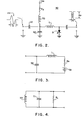
- a driver 10 that may be utilised for a short pulse generator in accordance with the present invention, comprises a charging circuit 11, a switching circuit 12, a pulse shaping circuit 13, and three capacitors C 1 , C 2 , and C 3 .
- the driver 10 further comprises transistors lla, llb, and llc coupled in parallel to respective diodes lld, lle, and llf.
- Each transistor lla, llb and llc may be of the type known in the art as MPS U10, whilst each of the diodes lld, lle and llf may be of the type known in the art as 1N914.
- junction of the cathode of the diode and the base of the transistors for the parallel pairs lla - lld, llb - lle, and llc - llf are coupled via resistors R 1a , R 1b , and R lc , respectively, and a terminal 14 to a power supply (not shown), whilst the junction of the emitter of the transistor and the anode of the diode of these transistor-diode pairs are respectively coupled to the capacitors C 1 , C 2 , and C 3 , and the collectors of the transistors lla, llb, and llc are respectively coupled to the terminal 14 via resistors R 2a , R 2b and R2c.
- Capacitors C 1 , C 2 , and C 3 are charged in parallel from the terminal 14 by current flowing through the corresponding transistors.
- the charging period is relatively rapid since thecurrent required for charging the capacitors is effectively multiplied by the ⁇ of the transistors.
- Current continues to flow through the transistors lla, llb and llc charging the capacitors C 1 , C 2 and C 3 until the leakage current through the diode, of each transistor-diode parallel combination, and the corresponding avalanche transistor of of the switch 12, as for example transistor 12a for the transistor diode parallel combination lla - lld, back biases the base of the transistor.
- the transistors lla, llb, and llc are turned off. This operation charges the capacitors C l , C 2 , and C 3 is parallel to the supply voltage at terminal 14, which may be 230 volts.
- the avalanche transistors 12a,12b and 12c are substantially at cut off, by virtue of a - 6V supply coupled to the gate thereof from terminals 16a, 16b, and 16c, via resistors R 3a , R 3b , and R 3c' respectively, only leakage current flowing therethrough.
- a positive trigger pulse from a series of positive trigger pulses 17 of width ⁇ 1 and height A, coupled via a terminal 18 and diodes 21 and 22 to the base of the transistor 12a causes the latter to avalanche, thereby placing the capacitor C 1 in series with the capacitor C 2 and establishing a voltage level at the anode of the diode lle that is the sum of the voltages across the capacitors C 1 and C 2 .
- This sum voltage causes the diode 11e to conduct, placing the sum voltage on the collector of the transistor 12b.
- the sum voltage over-volts the transistor 12b causing it to avalanche, thereby placing the three capacitors C 1 , C 2 , and C 3 in series and establishes a voltage at the anode of diode llf that causes it to conduct thereby coupling the sum voltage of all three capacitors to the base of the transistor 12c.
- the sum of the voltages across the three capacitors C 1 , C 2 and C 3 causes the transistor 12c to avalanche, thus completing the circuit to ground, via a pulse shaping network 13 which may be a length of coaxial cable, such as RG, 141/U, shorted at one end, wherethrough the capacitors C 1 , C 2 , and C 3 are discharged, thereby providing a pulse at an output terminal 23.
- the pulse shaper 13 which comprises a shorted coaxial line of length L2.
- Signals coupled to the pulse shaper 13 propagate to the shorted end thereof, experience a phase reversal thereat, and are reflected from the shorted end arriving at the input end after a time lapse of 2 l 2 /v 2 , where v 2 is the propagation velocity along the transmission line comprising the pulse shaper 13.
- the doublet pulse 24 will have a positive peak amplitude h 1 substantially equal to 120V, a negative peak amplitude h 2 substantially equal to 65V, and a total width ⁇ 2 substantially equal to four nanoseconds, one cycle of a 250 MHz wave, when, in addition to the parameters previously stated, the circuit components have the following values:
- a matching resistor R 6 may be coupled to the output terminal 23 when an output pulse that is substantially ring free is desired.
- This resistor when of appropriate value (generally 50 ohms), substantially eliminates multiple reflections between the transistor 12c and the output terminal 23. Though this resistor significantly improves the pulse shape at the output terminal 23, it concomitantly decreases the peak pulse amplitude thereat and should be used only when a substantially ring free output pulse is desired.
- the transistors 12a, 12b and 12c are cut off; transistors lla, llb, and llc are conducting; and capacitors C 1 , C 2 . and C 3 are being recharged to repeat the above described process upon the reception of a subsequent pulse in the pulse train 17.
- the doublet pulse 24 is coupled to a step recovery diode (SRD) 31 via a capacitor 32 and an inductance L.
- a negative bias voltage which may be -6 volts, is coupled via a terminal 34, a resistor R 7 and a choke inductance 35 to the SRD 31 to establish an initial non;conducting state.
- a capacitor 36 is coupled between ground and the junction of the choke 35 with the inductance L.
- the SRD 31 may be a MA 44483 manufactured by Microwave Associates of Burlington, Massachusetts.
- the reverse bias capacitance of this device is of the order of 1.4 picofarads.
- an impulse width of the order of picoseconds may be realised with an inductance L of 6 nanoseconds and a load resistance R of 50 ohms.
- parasitic capacitances cause the pulse width to be of the order of 400 picoseconds.
- the peak amplitude Ap of the pulse obtained with this circuit was of the order of 100 volts at a pulse repetition frequency of 100 KHz, the repetition frequency of the trigger pulse sequence.
Landscapes
- Generation Of Surge Voltage And Current (AREA)
- Electrotherapy Devices (AREA)
- Electrical Discharge Machining, Electrochemical Machining, And Combined Machining (AREA)
- Surgical Instruments (AREA)
Applications Claiming Priority (2)
| Application Number | Priority Date | Filing Date | Title |
|---|---|---|---|
| US378558 | 1982-05-17 | ||
| US06/378,558 US4442362A (en) | 1982-05-17 | 1982-05-17 | Short pulse generator |
Publications (3)
| Publication Number | Publication Date |
|---|---|
| EP0094765A2 true EP0094765A2 (fr) | 1983-11-23 |
| EP0094765A3 EP0094765A3 (en) | 1986-01-29 |
| EP0094765B1 EP0094765B1 (fr) | 1989-05-03 |
Family
ID=23493607
Family Applications (1)
| Application Number | Title | Priority Date | Filing Date |
|---|---|---|---|
| EP83302521A Expired EP0094765B1 (fr) | 1982-05-17 | 1983-05-05 | Générateur d'impulsion brève |
Country Status (5)
| Country | Link |
|---|---|
| US (1) | US4442362A (fr) |
| EP (1) | EP0094765B1 (fr) |
| JP (1) | JPS58206226A (fr) |
| DE (1) | DE3379824D1 (fr) |
| NO (1) | NO162836C (fr) |
Cited By (2)
| Publication number | Priority date | Publication date | Assignee | Title |
|---|---|---|---|---|
| EP2106025A1 (fr) * | 2008-03-27 | 2009-09-30 | Zachodniopomorksi Uniwersytet Technologiczny w Szczecinie | Procédé de formation d'une impulsion haute tension dans un module générateur et configuration du générateur haute tension |
| RU2682015C1 (ru) * | 2017-10-09 | 2019-03-14 | Акционерное общество "Федеральный научно-производственный центр "Нижегородский научно-исследовательский институт радиотехники" | Генератор импульсных напряжений |
Families Citing this family (22)
| Publication number | Priority date | Publication date | Assignee | Title |
|---|---|---|---|---|
| JPS59210721A (ja) * | 1983-05-14 | 1984-11-29 | Nec Corp | パルス発生回路 |
| JPS6118349A (ja) * | 1984-07-05 | 1986-01-27 | Mitsubishi Electric Corp | 超電導回転電機の回転子 |
| US4704543A (en) * | 1984-09-01 | 1987-11-03 | Marconi Company Limited | Pulse generator |
| US4651021A (en) * | 1985-08-05 | 1987-03-17 | Hawkey Dale F | Pulser circuit |
| US4727340A (en) * | 1986-04-30 | 1988-02-23 | Tektronix, Inc. | Comb generators |
| US4908526A (en) * | 1988-06-03 | 1990-03-13 | Harris Corporation | Pulse generator output voltage calibration circuit |
| US5274271A (en) * | 1991-07-12 | 1993-12-28 | Regents Of The University Of California | Ultra-short pulse generator |
| DE4324331A1 (de) * | 1993-07-20 | 1995-01-26 | Sokolov Vladimir Dipl El Ing | Vorrichtung zum Speisen einer elektrischen Last |
| US6355992B1 (en) | 1998-08-11 | 2002-03-12 | Utron Inc. | High voltage pulse generator |
| US6433720B1 (en) | 2001-03-06 | 2002-08-13 | Furaxa, Inc. | Methods, apparatuses, and systems for sampling or pulse generation |
| US6642878B2 (en) * | 2001-06-06 | 2003-11-04 | Furaxa, Inc. | Methods and apparatuses for multiple sampling and multiple pulse generation |
| US7286599B1 (en) * | 2003-03-06 | 2007-10-23 | Femto Devices, Inc. | Method and design of data communications transceiver for ultra wide band (UWB) operation in 3.1 GHz to 10.6 GHz frequency band |
| EP1528679B1 (fr) * | 2003-09-26 | 2014-01-15 | Krohne Messtechnik Gmbh & Co. Kg | Circuits d'impulsion et méthode pour générer des impulsions courtes |
| US7122999B1 (en) | 2004-02-23 | 2006-10-17 | Stangenes Industries, Inc. | Circuit for compensating rise times and ringing in high impedance loads |
| US8194715B2 (en) * | 2005-04-20 | 2012-06-05 | Agency For Science, Technology And Research | Apparatus and method for generating a monocycle |
| US7767433B2 (en) * | 2005-04-22 | 2010-08-03 | University Of Southern California | High voltage nanosecond pulse generator using fast recovery diodes for cell electro-manipulation |
| DE102008060663A1 (de) * | 2008-12-08 | 2010-06-10 | KROHNE Meßtechnik GmbH & Co. KG | Schaltungsanordnung zur Erzeugung kurzer elektrischer Impulse |
| JP5193098B2 (ja) * | 2009-03-05 | 2013-05-08 | 古河電気工業株式会社 | インパルス生成回路 |
| CN103947112B (zh) * | 2011-08-15 | 2017-06-09 | 尼泰克股份有限公司 | 雪崩脉冲发生器 |
| CN106877842A (zh) * | 2017-02-14 | 2017-06-20 | 华东师范大学 | 一种大幅度皮秒级窄脉冲发生电路 |
| RU189081U1 (ru) * | 2018-10-25 | 2019-05-13 | Акционерное Общество "Светлана-Электронприбор" | Формирователь сверхкоротких видеоимпульсов переменной длительности |
| GB2589604A (en) * | 2019-12-04 | 2021-06-09 | Creo Medical Ltd | Pulse generating circuit, and electrosurgical generator incorporating the same |
Family Cites Families (4)
| Publication number | Priority date | Publication date | Assignee | Title |
|---|---|---|---|---|
| US3513328A (en) * | 1968-05-06 | 1970-05-19 | Gen Electric | Pulse generating circuit utilizing avalanche firing of series connected scr's |
| US3878450A (en) * | 1970-04-29 | 1975-04-15 | Greatbatch W Ltd | Controlled voltage multiplier providing pulse output |
| US3832568A (en) * | 1973-08-10 | 1974-08-27 | Sperry Rand Corp | Circuit for generating a single high voltage subnanosecond pulse from a step recovery diode |
| US3997843A (en) * | 1975-06-20 | 1976-12-14 | Calspan Corporation | Monocycle pulse generator |
-
1982
- 1982-05-17 US US06/378,558 patent/US4442362A/en not_active Expired - Fee Related
-
1983
- 1983-05-05 DE DE8383302521T patent/DE3379824D1/de not_active Expired
- 1983-05-05 EP EP83302521A patent/EP0094765B1/fr not_active Expired
- 1983-05-12 JP JP58083452A patent/JPS58206226A/ja active Granted
- 1983-05-13 NO NO831729A patent/NO162836C/no unknown
Cited By (2)
| Publication number | Priority date | Publication date | Assignee | Title |
|---|---|---|---|---|
| EP2106025A1 (fr) * | 2008-03-27 | 2009-09-30 | Zachodniopomorksi Uniwersytet Technologiczny w Szczecinie | Procédé de formation d'une impulsion haute tension dans un module générateur et configuration du générateur haute tension |
| RU2682015C1 (ru) * | 2017-10-09 | 2019-03-14 | Акционерное общество "Федеральный научно-производственный центр "Нижегородский научно-исследовательский институт радиотехники" | Генератор импульсных напряжений |
Also Published As
| Publication number | Publication date |
|---|---|
| NO831729L (no) | 1983-11-18 |
| JPS58206226A (ja) | 1983-12-01 |
| DE3379824D1 (en) | 1989-06-08 |
| EP0094765A3 (en) | 1986-01-29 |
| JPH0480565B2 (fr) | 1992-12-18 |
| NO162836C (no) | 1990-02-21 |
| EP0094765B1 (fr) | 1989-05-03 |
| US4442362A (en) | 1984-04-10 |
| NO162836B (no) | 1989-11-13 |
Similar Documents
| Publication | Publication Date | Title |
|---|---|---|
| EP0094765B1 (fr) | Générateur d'impulsion brève | |
| US3832568A (en) | Circuit for generating a single high voltage subnanosecond pulse from a step recovery diode | |
| US4888556A (en) | Linear induction accelerator and pulse forming networks therefor | |
| US2469977A (en) | Pulser circuit | |
| US4160214A (en) | Modular modulator for radar transmitters | |
| US4822991A (en) | Optically switched microwave pulse generator | |
| Mazarakis et al. | A compact, high-voltage E-beam pulser | |
| US3171040A (en) | Fast charging circuit for pulse networks | |
| US3636476A (en) | Solid-state double resonant pulser | |
| US3041470A (en) | Horizontal sweep circuit for cathode-ray tube | |
| US3385982A (en) | High power solid state pulse generator with very short rise time | |
| US3611210A (en) | Sectionalized pulse modulator | |
| US3881120A (en) | Pulse generating circuit | |
| US3486043A (en) | High power pulse width modulator employing step recovery diodes | |
| US4536723A (en) | High-power pulse generator using transmission line with spark discharge device | |
| US3241076A (en) | Signal sampling circuit including a signal conductor disposed in the electromagneticfield of a shorted transmission line | |
| US3479528A (en) | High speed sample and hold circuit | |
| US2560576A (en) | Stabilized multivibrator | |
| US2474243A (en) | Line pulse modulator | |
| US5969439A (en) | Pulse generator apparatus for RF pulse generation in tuned loads including series regulation and capacitor clamping method therefor | |
| US4365287A (en) | Switching device | |
| EP0637133B1 (fr) | Appareil et procédé pour générer des impulsions répétitives | |
| US3333203A (en) | Pulse generator with standing wave energy storage | |
| RU2714739C1 (ru) | Неоднородная формирующая длинная линия (варианты) | |
| CN110907718A (zh) | 一种照明产品电磁兼容辐射骚扰标准样品 |
Legal Events
| Date | Code | Title | Description |
|---|---|---|---|
| PUAI | Public reference made under article 153(3) epc to a published international application that has entered the european phase |
Free format text: ORIGINAL CODE: 0009012 |
|
| AK | Designated contracting states |
Designated state(s): DE FR GB IT NL |
|
| PUAL | Search report despatched |
Free format text: ORIGINAL CODE: 0009013 |
|
| AK | Designated contracting states |
Designated state(s): DE FR GB IT NL |
|
| 17P | Request for examination filed |
Effective date: 19860317 |
|
| 17Q | First examination report despatched |
Effective date: 19870317 |
|
| ITF | It: translation for a ep patent filed | ||
| GRAA | (expected) grant |
Free format text: ORIGINAL CODE: 0009210 |
|
| AK | Designated contracting states |
Kind code of ref document: B1 Designated state(s): DE FR GB IT NL |
|
| REF | Corresponds to: |
Ref document number: 3379824 Country of ref document: DE Date of ref document: 19890608 |
|
| ET | Fr: translation filed | ||
| PLBE | No opposition filed within time limit |
Free format text: ORIGINAL CODE: 0009261 |
|
| RAP2 | Party data changed (patent owner data changed or rights of a patent transferred) |
Owner name: UNISYS CORPORATION |
|
| STAA | Information on the status of an ep patent application or granted ep patent |
Free format text: STATUS: NO OPPOSITION FILED WITHIN TIME LIMIT |
|
| 26N | No opposition filed | ||
| NLT2 | Nl: modifications (of names), taken from the european patent patent bulletin |
Owner name: UNISYS CORPORATION TE BLUE BELL, PENNSYLVANIE, VER |
|
| ITTA | It: last paid annual fee | ||
| PGFP | Annual fee paid to national office [announced via postgrant information from national office to epo] |
Ref country code: FR Payment date: 19940513 Year of fee payment: 12 |
|
| PGFP | Annual fee paid to national office [announced via postgrant information from national office to epo] |
Ref country code: NL Payment date: 19940531 Year of fee payment: 12 |
|
| PGFP | Annual fee paid to national office [announced via postgrant information from national office to epo] |
Ref country code: GB Payment date: 19950407 Year of fee payment: 13 |
|
| PGFP | Annual fee paid to national office [announced via postgrant information from national office to epo] |
Ref country code: DE Payment date: 19950531 Year of fee payment: 13 |
|
| PG25 | Lapsed in a contracting state [announced via postgrant information from national office to epo] |
Ref country code: NL Effective date: 19951201 |
|
| NLV4 | Nl: lapsed or anulled due to non-payment of the annual fee |
Effective date: 19951201 |
|
| PG25 | Lapsed in a contracting state [announced via postgrant information from national office to epo] |
Ref country code: FR Effective date: 19960229 |
|
| REG | Reference to a national code |
Ref country code: FR Ref legal event code: ST |
|
| REG | Reference to a national code |
Ref country code: FR Ref legal event code: ST |
|
| PG25 | Lapsed in a contracting state [announced via postgrant information from national office to epo] |
Ref country code: GB Effective date: 19960505 |
|
| GBPC | Gb: european patent ceased through non-payment of renewal fee |
Effective date: 19960505 |
|
| PG25 | Lapsed in a contracting state [announced via postgrant information from national office to epo] |
Ref country code: DE Effective date: 19970201 |