EP0095083A1 - Schaltung zur Gewinnung des Taktes einer binären, NRZ-kodierten Nachricht - Google Patents
Schaltung zur Gewinnung des Taktes einer binären, NRZ-kodierten Nachricht Download PDFInfo
- Publication number
- EP0095083A1 EP0095083A1 EP83104577A EP83104577A EP0095083A1 EP 0095083 A1 EP0095083 A1 EP 0095083A1 EP 83104577 A EP83104577 A EP 83104577A EP 83104577 A EP83104577 A EP 83104577A EP 0095083 A1 EP0095083 A1 EP 0095083A1
- Authority
- EP
- European Patent Office
- Prior art keywords
- clock
- message
- transitions
- output
- modulo
- Prior art date
- Legal status (The legal status is an assumption and is not a legal conclusion. Google has not performed a legal analysis and makes no representation as to the accuracy of the status listed.)
- Granted
Links
- 230000007704 transition Effects 0.000 claims abstract description 73
- 238000001514 detection method Methods 0.000 claims abstract description 29
- 238000000034 method Methods 0.000 claims abstract description 6
- 230000001360 synchronised effect Effects 0.000 claims abstract description 6
- 239000000654 additive Substances 0.000 claims description 7
- 230000000996 additive effect Effects 0.000 claims description 7
- 230000002123 temporal effect Effects 0.000 claims description 7
- 230000002401 inhibitory effect Effects 0.000 claims description 4
- 230000010354 integration Effects 0.000 description 4
- 238000010586 diagram Methods 0.000 description 3
- 238000012937 correction Methods 0.000 description 2
- 230000006870 function Effects 0.000 description 2
- 241000238876 Acari Species 0.000 description 1
- 206010003497 Asphyxia Diseases 0.000 description 1
- 238000013459 approach Methods 0.000 description 1
- 230000005540 biological transmission Effects 0.000 description 1
- 230000000295 complement effect Effects 0.000 description 1
- 230000003111 delayed effect Effects 0.000 description 1
- 230000008030 elimination Effects 0.000 description 1
- 238000003379 elimination reaction Methods 0.000 description 1
- 239000012464 large buffer Substances 0.000 description 1
- 238000012423 maintenance Methods 0.000 description 1
- 230000010363 phase shift Effects 0.000 description 1
- 238000012545 processing Methods 0.000 description 1
- 238000011084 recovery Methods 0.000 description 1
- 230000002441 reversible effect Effects 0.000 description 1
- 238000012360 testing method Methods 0.000 description 1
Images

Classifications
-
- H—ELECTRICITY
- H04—ELECTRIC COMMUNICATION TECHNIQUE
- H04L—TRANSMISSION OF DIGITAL INFORMATION, e.g. TELEGRAPHIC COMMUNICATION
- H04L7/00—Arrangements for synchronising receiver with transmitter
- H04L7/02—Speed or phase control by the received code signals, the signals containing no special synchronisation information
- H04L7/033—Speed or phase control by the received code signals, the signals containing no special synchronisation information using the transitions of the received signal to control the phase of the synchronising-signal-generating means, e.g. using a phase-locked loop
- H04L7/0331—Speed or phase control by the received code signals, the signals containing no special synchronisation information using the transitions of the received signal to control the phase of the synchronising-signal-generating means, e.g. using a phase-locked loop with a digital phase-locked loop [PLL] processing binary samples, e.g. add/subtract logic for correction of receiver clock
Definitions
- the present invention is in the field of digital transmissions and relates to the recovery of the clock defining the time intervals between which all the transitions of a binary message coded in NRZ lie.
- circuits for acquiring the clock of a binary message coded in NRZ comprise, as a general rule, a local clock, at the frequency of the clock of the binary message coded in expected NRZ, provided with a phase-locked loop tending to make the transitions of the binary message coincide with its beginnings of period.
- the loop is formed by a device for adjusting the phase of the local clock controlled by a comparator which detects the position of the transitions of the binary message coded in NRZ relative to the beginnings of the periods of the local clock. More or less sophisticated filters are inserted between the comparator and the phase adjustment device in order to obtain a very short acquisition time and a high insensitivity to interference.
- the clock acquisition capacity of a binary message is an important characteristic, in particular in the case where binary messages coded in NRZ are in the form of asynchronous trains and where any delay in clock acquisition can lead either data loss or the need to use a prohibitively large buffer.
- it is thwarted by the existence, for the phase control of the local clock, of an unstable equilibrium position which corresponds to a local clock in phase opposition with that of the message received and in which the control can be maintained for a certain time by a succession of alternating corrections of advance and phase delay.
- the elimination of the unstable equilibrium position from their phase control results from a detection consisting in verifying that there does not exist, in the message received, of transition in the vicinity of the middle of the periods of the local clock and, if not, of a brutal correction of phase causing the release of the phase control from its position of false equilibrium.
- the object of the present invention is to reduce the acquisition time of the clock of a message coded in NRZ by avoiding at the start of an acquisition procedure the possibility of reaching a false balance for the phase control of the local clock this, thanks to a pre-setting of the phase of the local clock on a more or less rough preliminary estimate of the phase of the clock of the received message carried out while the latter is passing through a delay line.
- the estimation of the modulo p rank of the class of time windows with which the beginnings of the periods of the clock of the received message coincide allows an initial setting of the local clock with a phase difference at most equal to 2 ⁇ / p, the number p is chosen so that this difference is small enough to eliminate the possibility of convergence of a phase control towards the false equilibrium position and even preferred to allow, with good probability, correct processing of the data of the message received.
- the census means advantageously consist of accounting means supplemented by calculation means delivering the distribution difference relating to time windows of the same modulo p rank as the current time window by operating by recurrence from the distribution difference calculated at price of the previous time window and the most recent values previously obtained for accounts relating to different classes of time windows.
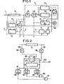
- the circuit shown in Figure 1 has an input 1 to which the asynchronous binary messages are applied and several outputs 2, 3 and 4. We find on an output 2 the messages applied to input 1 after a constant delay including the time d acquisition of the phases of their clocks, on another output 3 a binary signal D of modulation detection representative of the actual presence or not of a binary message at output 2 and on another output 4 the clock signal recovered from binary message available at output 2.
- It essentially comprises a local clock 5 at the frequency F of the clocks of the received messages slaved in phase on the transitions of the binary message available at output 2, a delay line 6 interposed between input 1 and the local clock 5 compensating for the phase acquisition time, and a rapid phase acquisition circuit 7 which detects a modulation, the initial synchronization of the local clock 5 and, indirectly, the control of its control mode.
- the local clock -5 is provided with a first order phase control loop with two integrating filters 54, 55 switched via a selector 56.
- One of the filters 54 has a time constant low to allow the passage of the zero phase difference in ten bits of a message but sufficient to ensure the stability of the convergence of the phase control beyond the performance of the fast phase acquisition circuit 7.
- the other filter 55 has a large time constant to allow the maintenance of the acquired phase even in the event of momentary loss or suffocation of the link but compatible with a slip at least equal to twice that expected between emission oscillators and reception.
- the low time constant filter 54 is in service in the absence of modulation detection and in the presence of modulation detection during the first bits of a message, the time to acquire a zero phase difference. It is then replaced by the other filter 55.
- the local clock 5 comprises, in a conventional manner, an oscillator 50 at a frequency F 'equal to an integer multiple r of the frequency F followed by a phase modulator produced with a divider by r 51 provided with a reset command to zero and a command allowing its division ratio to be changed from - 1.
- the reset command is used by the clock acquisition circuit 7 for the initial synchronization of the local clock.
- the command for modifying the division ratio r of t 1 is used by the phase-locked loop to cause, as necessary, a phase advance or delay of the local clock 5.
- the phase control loop of the local clock 5 comprises a transition detector 53 which receives as input the binary messages from the delay line 6 and delivers at its output pulses of short duration coinciding with the transitions of these messages .
- a phase comparator 54 with two inputs, one connected to the output of the divi programmable generator 51, the other to that of the transition detector 53, directs these pulses towards one or the other of its outputs A, R according to whether they are late or in phase advance with respect to the transitions d 'a given sense of the local clock signal considered as the start of a period.
- the integration filters 54, 55 connected to the two outputs of the comparator deliver on a two-bit output a signal for maintaining or correcting in advance or behind the phase of the signal of the local clock so as to balance the number of pulses on the two outputs of the phase comparator 54. They are for example with stochastic recurrence of the "N before M" type as described by JR CESSNA in an article published in the journal IEEE Transactions on Communications V O L. COM. 20 N ° 2, April 72, one with small N and M values giving it low inertia, the other with large N and M values giving it high inertia.
- the selector 56 activates one or other of the integration filters 54, 55. It can be controlled, as shown by means of a bistable 8 and a counter 9.
- the modulation detection signal D keeps the counter 9 at zero and the bistable in a so-called rest position corresponding to the selection of the integration filter 54 or 55 with a low time constant.
- the counter 9 counts the bits of this message and, having reached its maximum capacity, sends a switching pulse to the bistable 8 which changes state and selects the integration filter with a large time constant.
- the rapid phase acquisition circuit 7 essentially comprises two parts, one 71 ensuring the detection of a modulation, that is to say the presence of a message in transit in the delay line 6 transmitting a modulation detection signal D and the other 72 ensuring clock acquisition, that is to say an estimation of the initial phase of the message in transit in the delay line 6.
- the modulation detection circuit 71 can comprise a self-correlator with two inputs connected to the ends of the delay line 6 which calculates the autocorrelation value between two versions of the signal received in transit in the delay line 6 delayed one compared to each other half a clock period and a comparator to double threshold generating a binary signal D passing to a state corresponding to a modulation detection when the autocorrelation value delivered by the autocorrelator is greater than a lower threshold below which the received signal is considered to be noise and less at a higher threshold above which it is considered that there is absence of received signal.
- the clock acquisition circuit 72 generates from the signals at the ends of the delay line 6 , a binary clock initialization signal H i whose transitions from 0 to 1 approach the beginnings clock periods of a message in transit in the delay line 6 when such a message actually exists.
- This signal H i is applied to a monostable 73 which sends reset pulses from the programmable divider 51 of the local clock 5 when it is not blocked by the signal D of the modulation detection circuit, ie only at the start of each modulation detection and for a single trigger.
- the initial estimation of the clock phase of the received message is done by dividing the duration of a clock period into p successive time windows of the same duration, by grouping these windows by classes according to their rank modulo p with respect to to an arbitrary origin chosen locally and by determining the class of windows most often coinciding with the transitions of the message received, and stored in the delay line 6. This determination can be done simply by counting, during each time window, the number of transitions of the message stored in the delay line 6 having coincided with previous time windows of the same class modulo p and detecting whether this number is maximum.
- FIG. 2 illustrates the diagram of a clock acquisition circuit operating in this way. It has, in addition to its inputs 100, 101 by which it receives the signals present at the ends of the delay line 6, a timing input 102 on which it receives a timing signal H 1 defining the width of the time windows, having p times the frequency F and which can be obtained from the oscillator 50 of the local clock by an adequate ratio division.
- Two transition detectors 103, 104 are connected to the outputs mites of the delay line 6 and output pulses of the same width as a time window, synchronous transitions.
- a p-stage shift register 105 punctuated by the alignment signal H 1 plays the role of a circulating memory which stores the accounts of the transitions of the signal contained in the delay line 6 having occurred in the p classes of time windows .
- An adder 106 looped on itself via the shift register 105 ensures the updating of the various accounts. Besides its additive loopback input it has a unit increment input which is connected to the output of the transition detector 103 connected to the input of the delay line 6 and which allows the taking into account of each newly transition received, and a decrementing input of a unit which is connected to the output of the transition detector 104 connected to the output of the delay line 6 and which allows the counting of each transition of the signal leaving the delay line 6.
- a relative maximum detector outputs a binary signal at logic level 1 if the account of the modulo p class to which the current time window belongs is greater than the accounts of the modulo p classes of the time windows immediately preceding and following the time window in Classes. It consists of two comparators 107, 108 with two inputs connected one to the input and output of the first stage of the shift register 105 and the other to the input of the shift register 105 and the output of its top floor, and a logic gate of type "and" 103.
- a threshold comparator 110 connected to the output of the adder 110 blocks the output of the relative maximum detector via a logic gate of type "and" 111 in the case where the detected maximum does not exceed a certain threshold chosen according to the noise that could affect the received message.
- the detection of the modulo p class of time windows coinciding with the majority of the transitions of the message stored in the delay line 6 can also be done from the determination among the modulo p classes of time windows, of that with respect to the windows in which the transitions of the message are distributed most equally on both sides.
- This determination is less sensitive noises because it makes it possible to implement for each class most of the transitions of the message stored in the delay line 6 and not only those coinciding with the time windows of the class considered.
- it has the disadvantage of leading to uncertainty, the transitions being distributed in a balanced manner both on both sides of the class of windows with which they coincide for the most part and on both sides of the class of time windows with which they are mostly phase shifted by half a clock period.
- the advance domain coincides with the time windows whose classes have a modulo p rank less than the ith of at most p / 2 while that the delay domain coincides with the temporal windows whose classes have a rank modulo p greater than the ith at most p / 2.
- the class of windows of rank i must be excluded from or included therein according to whether the number p of time windows per clock period is odd or even.
- the transitions of the message in transit in the delay line 6 in advance with respect to the time windows of the class of rank i are those which coincided with time windows belonging to classes of rank j verifying conditions : while the transitions lagging behind the time windows of the class of rank i. are those which have coincided with time windows belonging to classes of rank j satisfying the conditions:
- the difference in distribution y i between the early and late phase transitions with respect to the windows. of time of the ith class is expressed as a function of the numbers x j of transitions coinciding with the time windows of a rank j by the expression: and can take the form: which brings up the expression of the difference in distribution y i-1 .
- the indices are to be considered modulo p: we get the recurrence formula:
- the number p of time windows per clock period is an even integer, it is necessary to include the windows of the class of rank i considered in one of the domains of advance or delay which amounts to taking as benchmarks of early or late for the transitions of the message the beginnings or the ends of the windows of the class of rank i. If the windows of this last class are put in the delay domain the recurrence formula becomes: while otherwise it becomes:
- FIG. 3 illustrates the diagram of a clock acquisition circuit which is adapted to the case of an odd number p of time windows per clock period and which implements the recurrence relation (1).
- This circuit comprises, like that of FIG. 2, two inputs 100, 101 connected to the ends of the delay line 6 and an input 102 receiving a timing signal H 1 which defines the width of the time windows and whose frequency is a multiple odd p of the frequency F obtained from the oscillator 50 by an adequate ratio division, a shift register with p stages 105 punctuated by the timing signal H playing the role of a circulating memory memorizing the accounts x i transitions of the message contained in the delay line 6 having occurred in the different modulo p classes of time windows, an adder 106 looped back on itself by means of the p-stage shift register 105 ensuring the updating accounts thanks to an increment input of a unit connected via a transition detector 103 to the input of the delay line 6 and to a decrement input of a connected unit via a transition detector 104 at the output of the delay line 6.
- a second shift register 120 with p stages punctuated by the alignment signal H 1 plays the role of a circulating memory preserving over a duration of a clock period the differences in distribution y calculated during p time windows previously passed .
- An adder 121 looped on itself via the first stage of the shift register 120 performs the calculation of the distribution difference y i between the transitions of the message in transit in the delay line 6 in advance and respectively in delay with respect to the class of time windows to which the current time window belongs. It implements for this the recurrence relation (1) and comprises for this purpose, in addition to its additive looping input.
- two other additive inputs connected one to the output of the last stage of the shift register 105 on which the account x i of the coinciding transitions is available with the class of windows of rank i modulo p to which the current time window belongs and the other at the exit of the first stage of the shift register 105 on which is available the account x i-1 of the transitions coinciding with the class of windows of rank i-1 modulo p, and a subtractive input connected via a multiplier by two 122 to the output of i + 1 ⁇ 2 (p + 1) th stage of shift register 105 on which the account is available x i + 1 ⁇ 2 (P + 1).
- the class modulo p of the time windows with respect to which the transitions of the message contained in the delay line 6 are distributed on both sides in the most equitable manner is that for which the difference in distribution there is minimum in absolute value .
- the search for this minimum is done by means of two extractor circuits of absolute value 123, 124 and of a comparator 125 with two inputs connected to their suite.
- the absolute value extractor circuit 123 is connected at the input to the output of the adder 121 where there is available the distribution difference y i relating to the class in modulo p of the current window while the absolute value extractor circuit 124 is connected as input to the output of the top floor of the shift register 120 where there is available the distribution difference y i + 1 relative to the class modulo p of the time window which will follow that in progress.
- Comparator 125 outputs a binary signal in logic state 1 as long as the distribution difference y i relative to the modulo p class of the current window is less in absolute value than that y i + 1 of the modulo p class of the time window that will follow.
- Two threshold comparators 126, 127 control the output of the comparator 125 via a logic gate of type "and" 128 delivering a clock initialization signal H i . Their function is to remove the doubt mentioned above.
- One of the threshold comparators 126 is connected at the input to the output of a stage of the shift register 120 whose rank is close to 1 ⁇ 4 (p-1) and outputs a binary signal in logic state 1 if the difference in distribution y that it receives from the shift register 120 is negative.
- the other threshold comparator 127 is connected to the output of a stage of the shift register 120 whose rank is close to 1 ⁇ 4 (3 p-1) and outputs a binary signal in logic state 1 if the difference distribution there that it receives from the shift register 120 is positive.
- the difference y present at the output of the shift register 120 of rank close to 1 ⁇ 4 (p-1) relates to a class of time windows having a rank less than rank i of the current time window of approximately? (p-1) and therefore preceding the time windows of rank i by about a quarter of a clock period.
- the distribution difference y i passes through a minimum in absolute value for the time windows of rank i, it is necessarily negative if these windows coincide with the majority of the transitions of the message, and necessarily positive if these windows are phase shifted by half -clock period compared to the majority of the transitions of the message. This state of affairs is used by the threshold comparator 126 to eliminate the detection of the absolute minimum corresponding to the false balance.
- the difference in distribution there present at the output of the shift register 120 of rank close to 1 ⁇ 4 (3P-1) relates to a class of time windows having a rank less than rank i of the current time window of approximately 1 ⁇ 4 ( 3p-1) or, taking into account the definition modulo p ranks, having a rank greater than rank i of the current time window of about 1 ⁇ 4 (p-1) and consequently following the time windows of rank i of about a quarter of a clock period.
- the difference in distribution y i passes through a minimum in absolute value for the time windows of rank i, it is necessarily positive if these windows are phase shifted by a half clock period with respect to the majority of the transitions of the message.
- the threshold comparator 127 This state of affairs is used by the threshold comparator 127 to eliminate the detection of the absolute minimum corresponding to the false balance.
- the clock initialization signal H i has transitions from 0 to 1 which only appear during time windows coinciding with the beginnings of the message clock periods and which are used for the initial synchronization of the local clock 5.
- the adder 121 is advantageously a digital circuit calculating in binary complement to two which gives a structure of great simplicity to the comparators with thresholds 126, 127 which only have to transmit or reverse the sign bit and the absolute value extractor circuits 123, 124 which only have to eliminate the sign bit.
Landscapes
- Engineering & Computer Science (AREA)
- Computer Networks & Wireless Communication (AREA)
- Signal Processing (AREA)
- Synchronisation In Digital Transmission Systems (AREA)
Applications Claiming Priority (2)
| Application Number | Priority Date | Filing Date | Title |
|---|---|---|---|
| FR8208546A FR2527031A1 (fr) | 1982-05-17 | 1982-05-17 | Circuit d'acquisition de l'horloge d'un message binaire code en nrz |
| FR8208546 | 1982-05-17 |
Publications (2)
| Publication Number | Publication Date |
|---|---|
| EP0095083A1 true EP0095083A1 (de) | 1983-11-30 |
| EP0095083B1 EP0095083B1 (de) | 1987-01-28 |
Family
ID=9274096
Family Applications (1)
| Application Number | Title | Priority Date | Filing Date |
|---|---|---|---|
| EP19830104577 Expired EP0095083B1 (de) | 1982-05-17 | 1983-05-10 | Schaltung zur Gewinnung des Taktes einer binären, NRZ-kodierten Nachricht |
Country Status (6)
| Country | Link |
|---|---|
| EP (1) | EP0095083B1 (de) |
| DE (1) | DE3369620D1 (de) |
| DK (1) | DK160171C (de) |
| FR (1) | FR2527031A1 (de) |
| GR (1) | GR78569B (de) |
| IE (1) | IE54411B1 (de) |
Cited By (1)
| Publication number | Priority date | Publication date | Assignee | Title |
|---|---|---|---|---|
| EP0351072A3 (de) * | 1988-07-14 | 1992-02-05 | International Business Machines Corporation | Digitale Phasenregeleinrichtung und Verfahren dazu |
Citations (3)
| Publication number | Priority date | Publication date | Assignee | Title |
|---|---|---|---|---|
| US3851101A (en) * | 1974-03-04 | 1974-11-26 | Motorola Inc | Adaptive phase synchronizer |
| FR2283592A1 (fr) * | 1974-08-27 | 1976-03-26 | Thomson Csf | Dispositif extracteur de synchronisation et systeme de transmission d'informations comportant un tel dispositif |
| EP0020205A1 (de) * | 1979-06-01 | 1980-12-10 | Thomson-Csf | Vorrichtung zur Synchronisierung eines Taktsignals und synchrones Datenübertragungssystem mit einer solchen Vorrichtung |
-
1982
- 1982-05-17 FR FR8208546A patent/FR2527031A1/fr active Granted
-
1983
- 1983-05-10 EP EP19830104577 patent/EP0095083B1/de not_active Expired
- 1983-05-10 DE DE8383104577T patent/DE3369620D1/de not_active Expired
- 1983-05-16 DK DK217383A patent/DK160171C/da not_active IP Right Cessation
- 1983-05-16 IE IE113583A patent/IE54411B1/en not_active IP Right Cessation
- 1983-05-17 GR GR71372A patent/GR78569B/el unknown
Patent Citations (3)
| Publication number | Priority date | Publication date | Assignee | Title |
|---|---|---|---|---|
| US3851101A (en) * | 1974-03-04 | 1974-11-26 | Motorola Inc | Adaptive phase synchronizer |
| FR2283592A1 (fr) * | 1974-08-27 | 1976-03-26 | Thomson Csf | Dispositif extracteur de synchronisation et systeme de transmission d'informations comportant un tel dispositif |
| EP0020205A1 (de) * | 1979-06-01 | 1980-12-10 | Thomson-Csf | Vorrichtung zur Synchronisierung eines Taktsignals und synchrones Datenübertragungssystem mit einer solchen Vorrichtung |
Non-Patent Citations (1)
| Title |
|---|
| 1968 IEEE INTERNATIONAL CONFERENCE ON COMMUNICATIONS, CONFERENCE RECORD, vol. IV, IEEE Cat. no. 68C20-COM, 1968, pages 776-781, IEEE, New York, USA * |
Cited By (1)
| Publication number | Priority date | Publication date | Assignee | Title |
|---|---|---|---|---|
| EP0351072A3 (de) * | 1988-07-14 | 1992-02-05 | International Business Machines Corporation | Digitale Phasenregeleinrichtung und Verfahren dazu |
Also Published As
| Publication number | Publication date |
|---|---|
| GR78569B (de) | 1984-09-27 |
| FR2527031B1 (de) | 1984-12-07 |
| DK217383A (da) | 1983-11-18 |
| IE831135L (en) | 1983-11-17 |
| DK160171C (da) | 1991-07-01 |
| DK160171B (da) | 1991-02-04 |
| DE3369620D1 (en) | 1987-03-05 |
| DK217383D0 (da) | 1983-05-16 |
| IE54411B1 (en) | 1989-09-27 |
| FR2527031A1 (fr) | 1983-11-18 |
| EP0095083B1 (de) | 1987-01-28 |
Similar Documents
| Publication | Publication Date | Title |
|---|---|---|
| EP0013990B1 (de) | Verfahren zur serienförmigen Übertragung binärer Informationen und Vorrichtungen zur Durchführung des Verfahrens | |
| FR2498032A1 (fr) | Synchroniseur de bits pour signaux numeriques | |
| FR2664770A1 (fr) | Procede et systeme de transmission numerique de donnees en serie. | |
| EP0013343A1 (de) | Verfahren und Vorrichtung zur Auffindung einer Pseudo-Zufallsfolge von 0 Grad- und 180 Grad-Phasenänderungen der Trägerwelle in einem Datenempfänger | |
| EP0023852B1 (de) | Verfahren und Vorrichtung zur Phasenregelung eines lokalen Taktgebers | |
| FR2509890A1 (fr) | Appareil de lecture de donnees pour la transmission de donnees | |
| EP0400520B1 (de) | Schaltungsanordnung zur Detektion des Verlustes eines digitalen, empfangenen Signals für digitale Signalempfänger | |
| FR2615677A1 (fr) | Circuit de boucle de verrouillage de phase numerique | |
| EP0012880B1 (de) | Verfahren zum Dekodieren phasenkodierter, frequenzmoduliert kodierter oder in modifizierter Frequenzmodulation kodierter Binärdaten | |
| EP0466593B1 (de) | Datenabtastschaltung und ein digitales Datenübertragungssystem dazu | |
| EP0095083B1 (de) | Schaltung zur Gewinnung des Taktes einer binären, NRZ-kodierten Nachricht | |
| EP1101316B1 (de) | Verfahren zur taktrückgewinnung während der abtastung von digitalen signalen | |
| EP1163771B1 (de) | Synchroner bpsk dekodierer | |
| EP0031762A2 (de) | Modulator-Demodulator zur Übertragung durch eine vierpegelige doppelte Amplitudenmodulation auf Quadraturträgern | |
| FR2764147A1 (fr) | Procede et dispositif de recuperation de synchronisation sur un signal transmis a un recepteur de telephone mobile | |
| EP0526359B1 (de) | Verfahren und Schaltungsanordnung zur Synchronisierung eines Signals | |
| EP0109658A1 (de) | Synchrone Datenübertragungsanlage | |
| FR2725098A1 (fr) | Dispositif de synchronisation de branches d'un decodeur de viterbi compris dans un recepteur de donnees numeriques codees en treillis multidimensionnel | |
| EP0056208A1 (de) | Verfahren und Einrichtung zur Synchronisation von Nachrichten | |
| FR2646742A1 (fr) | Dispositif pour synchroniser un signal pseudo-binaire avec un signal d'horloge regeneree a sauts de phase | |
| FR2598869A1 (fr) | Detecteur de phase et de frequence, et son utilisation dans une boucle a verrouillage de phase | |
| FR2623675A1 (fr) | Dispositif de synchronisation d'une horloge par rapport a un signal numerique incident, notamment a haut debit | |
| FR2722051A1 (fr) | Procede et dispositif de donnees asynchrones sur un signal numerique | |
| EP0905946B1 (de) | Reglung der Abtastung von Biphasensignalen | |
| EP0092879A2 (de) | Bitsynchronisiereinrichtung für Modulator-Demodulator oder Empfänger von Datenübertragung |
Legal Events
| Date | Code | Title | Description |
|---|---|---|---|
| PUAI | Public reference made under article 153(3) epc to a published international application that has entered the european phase |
Free format text: ORIGINAL CODE: 0009012 |
|
| AK | Designated contracting states |
Designated state(s): BE DE FR GB IT LU NL |
|
| 17P | Request for examination filed |
Effective date: 19840524 |
|
| GRAA | (expected) grant |
Free format text: ORIGINAL CODE: 0009210 |
|
| AK | Designated contracting states |
Kind code of ref document: B1 Designated state(s): BE DE FR GB IT LU NL |
|
| ITF | It: translation for a ep patent filed | ||
| REF | Corresponds to: |
Ref document number: 3369620 Country of ref document: DE Date of ref document: 19870305 |
|
| PLBE | No opposition filed within time limit |
Free format text: ORIGINAL CODE: 0009261 |
|
| STAA | Information on the status of an ep patent application or granted ep patent |
Free format text: STATUS: NO OPPOSITION FILED WITHIN TIME LIMIT |
|
| 26N | No opposition filed | ||
| PGFP | Annual fee paid to national office [announced via postgrant information from national office to epo] |
Ref country code: GB Payment date: 19920427 Year of fee payment: 10 |
|
| PGFP | Annual fee paid to national office [announced via postgrant information from national office to epo] |
Ref country code: DE Payment date: 19920502 Year of fee payment: 10 |
|
| PGFP | Annual fee paid to national office [announced via postgrant information from national office to epo] |
Ref country code: LU Payment date: 19920513 Year of fee payment: 10 |
|
| PGFP | Annual fee paid to national office [announced via postgrant information from national office to epo] |
Ref country code: BE Payment date: 19920518 Year of fee payment: 10 |
|
| PGFP | Annual fee paid to national office [announced via postgrant information from national office to epo] |
Ref country code: FR Payment date: 19920521 Year of fee payment: 10 |
|
| ITTA | It: last paid annual fee | ||
| PGFP | Annual fee paid to national office [announced via postgrant information from national office to epo] |
Ref country code: NL Payment date: 19920531 Year of fee payment: 10 |
|
| EPTA | Lu: last paid annual fee | ||
| PG25 | Lapsed in a contracting state [announced via postgrant information from national office to epo] |
Ref country code: LU Free format text: LAPSE BECAUSE OF NON-PAYMENT OF DUE FEES Effective date: 19930510 Ref country code: GB Effective date: 19930510 |
|
| PG25 | Lapsed in a contracting state [announced via postgrant information from national office to epo] |
Ref country code: BE Effective date: 19930531 |
|
| BERE | Be: lapsed |
Owner name: SINTRA-ALCATEL Effective date: 19930531 |
|
| PG25 | Lapsed in a contracting state [announced via postgrant information from national office to epo] |
Ref country code: NL Effective date: 19931201 |
|
| GBPC | Gb: european patent ceased through non-payment of renewal fee |
Effective date: 19930510 |
|
| NLV4 | Nl: lapsed or anulled due to non-payment of the annual fee | ||
| PG25 | Lapsed in a contracting state [announced via postgrant information from national office to epo] |
Ref country code: FR Effective date: 19940131 |
|
| PG25 | Lapsed in a contracting state [announced via postgrant information from national office to epo] |
Ref country code: DE Effective date: 19940201 |
|
| REG | Reference to a national code |
Ref country code: FR Ref legal event code: ST |