EP0095372B1 - Optimale Oberflächenkrümmung zur thermischen Überleitung durch Konduktion eines dünnen flexiblen Werkstücks - Google Patents
Optimale Oberflächenkrümmung zur thermischen Überleitung durch Konduktion eines dünnen flexiblen Werkstücks Download PDFInfo
- Publication number
- EP0095372B1 EP0095372B1 EP83302955A EP83302955A EP0095372B1 EP 0095372 B1 EP0095372 B1 EP 0095372B1 EP 83302955 A EP83302955 A EP 83302955A EP 83302955 A EP83302955 A EP 83302955A EP 0095372 B1 EP0095372 B1 EP 0095372B1
- Authority
- EP
- European Patent Office
- Prior art keywords
- disc
- wafer
- contour
- contact surface
- contact
- Prior art date
- Legal status (The legal status is an assumption and is not a legal conclusion. Google has not performed a legal analysis and makes no representation as to the accuracy of the status listed.)
- Expired
Links
Images

Classifications
-
- H—ELECTRICITY
- H10—SEMICONDUCTOR DEVICES; ELECTRIC SOLID-STATE DEVICES NOT OTHERWISE PROVIDED FOR
- H10P—GENERIC PROCESSES OR APPARATUS FOR THE MANUFACTURE OR TREATMENT OF DEVICES COVERED BY CLASS H10
- H10P72/00—Handling or holding of wafers, substrates or devices during manufacture or treatment thereof
- H10P72/70—Handling or holding of wafers, substrates or devices during manufacture or treatment thereof for supporting or gripping
- H10P72/76—Handling or holding of wafers, substrates or devices during manufacture or treatment thereof for supporting or gripping using mechanical means, e.g. clamps or pinches
- H10P72/7604—Handling or holding of wafers, substrates or devices during manufacture or treatment thereof for supporting or gripping using mechanical means, e.g. clamps or pinches the wafers being placed on a susceptor, stage or support
- H10P72/7606—Handling or holding of wafers, substrates or devices during manufacture or treatment thereof for supporting or gripping using mechanical means, e.g. clamps or pinches the wafers being placed on a susceptor, stage or support characterised by edge clamping, e.g. clamping ring
-
- H—ELECTRICITY
- H01—ELECTRIC ELEMENTS
- H01J—ELECTRIC DISCHARGE TUBES OR DISCHARGE LAMPS
- H01J37/00—Discharge tubes with provision for introducing objects or material to be exposed to the discharge, e.g. for the purpose of examination or processing thereof
- H01J37/30—Electron-beam or ion-beam tubes for localised treatment of objects
- H01J37/317—Electron-beam or ion-beam tubes for localised treatment of objects for changing properties of the objects or for applying thin layers thereon, e.g. for ion implantation
-
- H—ELECTRICITY
- H10—SEMICONDUCTOR DEVICES; ELECTRIC SOLID-STATE DEVICES NOT OTHERWISE PROVIDED FOR
- H10P—GENERIC PROCESSES OR APPARATUS FOR THE MANUFACTURE OR TREATMENT OF DEVICES COVERED BY CLASS H10
- H10P72/00—Handling or holding of wafers, substrates or devices during manufacture or treatment thereof
- H10P72/70—Handling or holding of wafers, substrates or devices during manufacture or treatment thereof for supporting or gripping
- H10P72/76—Handling or holding of wafers, substrates or devices during manufacture or treatment thereof for supporting or gripping using mechanical means, e.g. clamps or pinches
- H10P72/7604—Handling or holding of wafers, substrates or devices during manufacture or treatment thereof for supporting or gripping using mechanical means, e.g. clamps or pinches the wafers being placed on a susceptor, stage or support
- H10P72/7611—Handling or holding of wafers, substrates or devices during manufacture or treatment thereof for supporting or gripping using mechanical means, e.g. clamps or pinches the wafers being placed on a susceptor, stage or support characterised by edge profile or support profile
Definitions
- the invention is related to heat transport involving objects and thermal reservoirs, and in particular, to cooling of semiconductor wafers subject to processing by ion implantation, sputtering or like processes.
- heat developed in the workpiece may become a limiting factor for the process.
- an upper limit on the workpiece temperature is recognized for several reasons. Where the wafer is coated with a resist layer as part of a lithographic process, deterioration or alteration of that layer will occur for temperatures elevated much in excess of 100°C. Wafers subject to prolonged irradiation may also experience undesirable diffusion of previously formed regions of distinct incremental properties within the semiconductor or a premature annealing of previously bombarded regions may occur.
- the aforementioned art relies upon a conductive mechanism for thermal transport. Thermal energy is developed in proximity to the outer surface of the wafer from the kinetic energy of the incident beam which is absorbed by the wafer. There is, therefore, a first component of thermal conductivity implicit in the thermal conductance properties of the wafer material because of the necessity of heat transport through the wafer material. (It will be assumed for simplicity that the thermal path is through the thickness of the wafer). Similarly, the platen exhibits thermal conductance properties characteristic of the material comprising the platen in effecting heat transfer between the surface of the platen in contact with the wafer, thence through the interior regions of the platen wherein cooling channels are disposed for circulating cooling fluids.
- thermal conductance in this region is nearly proportional to the actual contact area between the wafer and platen and inversely proportional to the mean thermal conductivity of the two materials.
- the surfaces are quite nonplanar and of irregular orientation; on the basis of certain assumptions of the hardness of materials and surface topography distributions of the respective contact surfaces, the contact area is calculable for microscopic measurement and is, in fact, but a small fraction of the macroscopic area.
- the theory of conductive heat transport between solid bodies in a vacuum is developed by Cooper, Mikic and Yovanovich, Int. J. Heat and Mass Transfer, vol. 12 pp.
- a surface layer which deforms to accommodate some portion of the small scale irregularities of the wafer.
- a further geometrical attribute in the length of the thermal path through the compliant material which length is proportionately shortened as the contact pressure increases. This effect appears in first order but is quite small for the small deformations usually encountered.
- FIG. 1 illustrates a typical ion implantation system.
- a high voltage terminal 2 is maintained at a selectable potential of +10 kev to +200 kev, typically, with respect to ground.
- an ion source 8 and associated power supplies 10 providing extraction probe and focusing potentials which need not be considered in detail for the present purposes.
- the ion source operates on a gaseous feed stock requiring gas handling system 6 which may be employed to select among several gas cylinders and to supply the selected gas to the ion source through a controlled leak.
- a high current ion beam 18 diverging from the ion source 8 is momentum analyzed in analyzer magnet 20 and issues from the magnet defined by aperture 22 and further limited by variable slit system 24.
- the beam is then accelerated to ground potential in accelerating tube 26.
- Optical elements 28 such as a quadrapole doublet, operate on the beam to yield a spatial momentum focus at the target planes 56 or 58.
- the typical system of Fig. 1 utilizes an electrostatic deflection system including y deflection plates 40 and x deflection plates 42 to direct the beam 18 over the selected target plane.
- the waveforms are developed in scan system 44 for application to the plates 40 and 42 to achieve a desired scanning pattern.
- a dual channel target chamber 46 is provided to house the workpiece(s) subject to processing.
- An automatic wafer handling system including feed channels 52 and 54 service the two processing channels for introducing semiconductor wafers, one at a time through each of two vacuum locks for time-staggered introduction into the target chamber.
- the wafer handling system properly locates, aligns, and cools the wafer during processing and removes the processed wafer from the chamber at the conclusion of processing.
- the wafer handling system is described in EP-A-0 095 368.
- the entire region traversed by the ion beam is maintained at high vacuum, e.g., typically pressures of the order of 1.33x10⁴-Pa (10- 6 mm.hg).
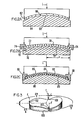
- clamping force L applied at the periphery of the wafer 62 may result in a non-uniform distribution of contact forces over the surface of the wafer. This results in a non-uniform loading of the wafer where the load is defined by the platen 64 of arbitrary convex surface contour 65.
- the local stress is represented symbolically by stylized vector components 66, one of which is so labeled.
- the thermal conductance of the interface between wafer 62 and platen 64 is a function of the contact force exerted on the wafer against the platen and the thermal and mechanical properties of the materials.
- the deflection described by equation (1) above fulfills one criteria for optimized contact cooling perceived in this work, e.g., uniform contact pressure distribution applied to the wafer.
- Limits are imposed on the maximum contact force by properties of the wafer material. As the wafer is deformed against a convex surface, the tangential stress components (tangential with respect to the normal contact forces) place the wafer under compression near its inner surface and under tension near its outer (convex) surface due to imposed bending. The respective surface tangential stress components exhibit a magnitude which delimit the design parameters, (especially the tensile stress at the outer surface).
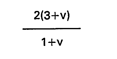
- a dimensionless expression is formed by dividing equation 1 by equation 3 which describes the desired contour for the platen.
- Equation 4 therefore expresses the concurrent conditions which yield uniformity of heat transfer over the surface of the wafer and maximum heat transfer from the wafer. It is noted that equation 4 has no dependence on Young's modulus and that Poisson's ratio varies little within a wide class of materials. Equation 4 expresses a uniformly applicable contour for the proposed purpose. In actual use the value of Y max imposes a constraint on the amplitude or scale of the curve, but it is noted that again a variety of different wafer materials may be accommodated without substantial sacrifice of thermal transfer properties.
- the platen 70 has a surface contour 71 according to equation 4.
- the wafer 72 is urged against the platen 70 by peripheral clamping ring 74 under a clamping force L.
- Cooling channels 76 are provided in the platen for the further removal of heat.
- the stress distribution represented symbolically by vector component 78 is observed to be uniform over the wafer as a result of the boundary condition of peripheral clamping and the uniform contact pressure loading imposed by conformance of the wafer 72 with the contour 71.
- the contact pressure will assume a value which does not change for further increase in L. Further increase in contact force AL is simply transmitted through the wafer to the substrate without affecting the distributed load.
- the platen assembly may comprise a rigid member 80 and a compliant thermally conductive coating 82.
- the intermediate contour 90 of the rigid member 80 is determined taking into consideration the properties of the compliant material 82 and the load to which the wafer 86 will be subject in order that the interface contour 84 between wafer 86 and platen 80, under the design load conditions, will conform to that desired contour yielding a contact pressure distribution which is uniform over the surface of the platen-wafer interface for the boundary conditions determined by the clamping of the wafer to the platen.
- the compliant layer exhibits a uniform thickness bonded to the intermediate contour 90 with the result that the interface contour 84 and intermediate contour 90 will be substantially identical.
- a compressed compliant layer may exhibit a radial thickness distribution due to increased perimeter loading, requiring a complex design procedure.
- Such design is most easily accomplished by an interative procedure in a computer model for which the function y i (r, 8) representing intermediate contour 90 of the bare platen is varied to yield the desired outer contour, y o (r, 8), taking account of the deformation of the compliant layer 82.
- the 6 dependence vanishes and these functions have radial symmetry.
- a tensile bending stress of 563 kg/cm 2 is tolerable.
- a maximum deflection of 0.1343 cm is taken as the amplitude of the contour given by equation 4.
- a contact pressure of 47 gm/cm 2 is maintained against an aluminum (6061-T6) heat sink so contoured.
- the thermal contact resistance is found to be about 65°C/watt/cm2 in vacuum.
- the aluminum platen body, the compliant substrate and the typical wafer contribute, respectively, 0.31, 2.11 and 0.033-0.074°C/watt/cm 2 .
- the contact impedance is the dominant contribution to the total thermal impedance, but the actual value of the thermal contact resistance is quite dependent upon the surface properties of the heat sink and wafer.
- Soft aluminum or indium are believed to offer excellent properties for this purpose.
- Pliable materials offer good properties with the possible advantage of tolerating surface dust.
- Gas may be introduced within the wafer-platen interface region to a pressure approximately equal to the contact pressure for enhanced heat transfer.
- This subject material is described in US-A-4 457 359.
- Alternative clamping arrangements may also be considered.
- One such alternative clamping arrangement will apply equal clamping forces L to the wafer at discrete points symmetrically disposed, as shown for example in Fig. 3, at three points equally spaced along the periphery of the wafer.
- a complex saddle-shaped contour will result. That is, the wafer will be deformed with a surface y(r, 6) where a is the azimuthal angle around the periphery.
- a surface may be computed with reference to Marguerre and Woernle, above referenced.
- the platen 108 is provided with such a saddle-shaped contour further constrained by the maximum deflection condition.
- the achievement of the complex contour required may readily be obtained using modern multiple axis machining techniques.
- the platen 108 may be so formed as in the aforedescribed embodiment with a compliant layer to facilitate the desired contour with the more complex computations so required.
- An advantage obtained in this discrete clamping embodiment is the additional wafer area accessible for production of devices on the wafer.
- the fractional surface area given over to a continuous peripheral clamp of width w is which is of the order of a few percent for typical values of w (2 mm) and r..
Landscapes
- Chemical & Material Sciences (AREA)
- Analytical Chemistry (AREA)
- Container, Conveyance, Adherence, Positioning, Of Wafer (AREA)
Claims (9)


Applications Claiming Priority (4)
| Application Number | Priority Date | Filing Date | Title |
|---|---|---|---|
| US38166882A | 1982-05-25 | 1982-05-25 | |
| US381670 | 1982-05-25 | ||
| US06/381,670 US4458746A (en) | 1982-05-25 | 1982-05-25 | Optimum surface contour for conductive heat transfer with a thin flexible workpiece |
| US381668 | 1982-05-25 |
Publications (3)
| Publication Number | Publication Date |
|---|---|
| EP0095372A2 EP0095372A2 (de) | 1983-11-30 |
| EP0095372A3 EP0095372A3 (en) | 1986-03-19 |
| EP0095372B1 true EP0095372B1 (de) | 1989-08-30 |
Family
ID=27009477
Family Applications (1)
| Application Number | Title | Priority Date | Filing Date |
|---|---|---|---|
| EP83302955A Expired EP0095372B1 (de) | 1982-05-25 | 1983-05-23 | Optimale Oberflächenkrümmung zur thermischen Überleitung durch Konduktion eines dünnen flexiblen Werkstücks |
Country Status (2)
| Country | Link |
|---|---|
| EP (1) | EP0095372B1 (de) |
| DE (1) | DE3380505D1 (de) |
Families Citing this family (1)
| Publication number | Priority date | Publication date | Assignee | Title |
|---|---|---|---|---|
| JPH06204323A (ja) * | 1992-10-27 | 1994-07-22 | Applied Materials Inc | ウェハプロセスチャンバ内のドーム状加熱ペディスタルのためのクランプリング |
Family Cites Families (2)
| Publication number | Priority date | Publication date | Assignee | Title |
|---|---|---|---|---|
| GB1443215A (en) * | 1973-11-07 | 1976-07-21 | Mullard Ltd | Electrostatically clamping a semiconductor wafer during device manufacture |
| US4282924A (en) * | 1979-03-16 | 1981-08-11 | Varian Associates, Inc. | Apparatus for mechanically clamping semiconductor wafer against pliable thermally conductive surface |
-
1983
- 1983-05-23 DE DE8383302955T patent/DE3380505D1/de not_active Expired
- 1983-05-23 EP EP83302955A patent/EP0095372B1/de not_active Expired
Also Published As
| Publication number | Publication date |
|---|---|
| DE3380505D1 (en) | 1989-10-05 |
| EP0095372A2 (de) | 1983-11-30 |
| EP0095372A3 (en) | 1986-03-19 |
Similar Documents
| Publication | Publication Date | Title |
|---|---|---|
| US4535835A (en) | Optimum surface contour for conductive heat transfer with a thin flexible workpiece | |
| US4458746A (en) | Optimum surface contour for conductive heat transfer with a thin flexible workpiece | |
| US4537244A (en) | Method for optimum conductive heat transfer with a thin flexible workpiece | |
| US4457359A (en) | Apparatus for gas-assisted, solid-to-solid thermal transfer with a semiconductor wafer | |
| KR102303060B1 (ko) | 웨이퍼 지지 디바이스 및 그 제조 방법 그리고 반도체 가공 장치 | |
| TWI283015B (en) | A method for molding a polymer surface that reduces particle generation and surface adhesion forces while maintaining a high heat transfer coefficient | |
| EP0244137B1 (de) | Verarbeitung einer Halbleiterscheibe | |
| EP0546842B1 (de) | Verfahren und Geräte zur Einschränkung des Plasma-Ätzgebietes zur Erlangung präziser Formgestaltung von Substratöberflächen | |
| US4282924A (en) | Apparatus for mechanically clamping semiconductor wafer against pliable thermally conductive surface | |
| GB2114813A (en) | Apparatus for thermal treatment of semiconductor wafers by gas conduction incorporating peripheral gas inlet | |
| US5548470A (en) | Characterization, modeling, and design of an electrostatic chuck with improved wafer temperature uniformity | |
| JP4079992B2 (ja) | 導電性被処理体を載置部材に締め付けるための装置及び静電クランピング方法 | |
| US4671204A (en) | Low compliance seal for gas-enhanced wafer cooling in vacuum | |
| US20050045106A1 (en) | Electrostatic chuck having a low level of particle generation and method of fabricating same | |
| EP3171393A1 (de) | Versiegelte si-elektroden mit elastomerbindung und dergleichen für verminderte partikelkontamination bel der dielektrischen ätzung | |
| US6909588B2 (en) | Substrate holder for retaining a substrate within a processing chamber | |
| WO2009064974A2 (en) | Embossed electrostatic chuck | |
| EP0452779B1 (de) | Klemmechanismus für physikalische Dampfniederschlagvorrichtung | |
| EP0030465B1 (de) | Elektronenstrahl-Bestrahlungsvorrichtung | |
| JP2026507457A (ja) | 正確な基板間結合のための応力管理 | |
| US5509464A (en) | Method and apparatus for cooling rectangular substrates | |
| EP0095372A2 (de) | Optimale Oberflächenkrümmung zur thermischen Überleitung durch Konduktion eines dünnen flexiblen Werkstücks | |
| US7595972B2 (en) | Clamp for use in processing semiconductor workpieces | |
| WO2004027839A2 (en) | Electrostatic chuck having a low level of particle generation and method of fabricating same | |
| JPH0670897B2 (ja) | 薄く柔軟な物品から熱を除去する装置 |
Legal Events
| Date | Code | Title | Description |
|---|---|---|---|
| PUAI | Public reference made under article 153(3) epc to a published international application that has entered the european phase |
Free format text: ORIGINAL CODE: 0009012 |
|
| AK | Designated contracting states |
Designated state(s): CH DE FR GB LI |
|
| PUAL | Search report despatched |
Free format text: ORIGINAL CODE: 0009013 |
|
| AK | Designated contracting states |
Kind code of ref document: A3 Designated state(s): CH DE FR GB LI |
|
| 17P | Request for examination filed |
Effective date: 19860905 |
|
| 17Q | First examination report despatched |
Effective date: 19880203 |
|
| GRAA | (expected) grant |
Free format text: ORIGINAL CODE: 0009210 |
|
| AK | Designated contracting states |
Kind code of ref document: B1 Designated state(s): CH DE FR GB LI |
|
| REF | Corresponds to: |
Ref document number: 3380505 Country of ref document: DE Date of ref document: 19891005 |
|
| ET | Fr: translation filed | ||
| PLBE | No opposition filed within time limit |
Free format text: ORIGINAL CODE: 0009261 |
|
| STAA | Information on the status of an ep patent application or granted ep patent |
Free format text: STATUS: NO OPPOSITION FILED WITHIN TIME LIMIT |
|
| 26N | No opposition filed | ||
| PGFP | Annual fee paid to national office [announced via postgrant information from national office to epo] |
Ref country code: CH Payment date: 19960429 Year of fee payment: 14 |
|
| PG25 | Lapsed in a contracting state [announced via postgrant information from national office to epo] |
Ref country code: LI Free format text: LAPSE BECAUSE OF NON-PAYMENT OF DUE FEES Effective date: 19970531 Ref country code: CH Free format text: LAPSE BECAUSE OF NON-PAYMENT OF DUE FEES Effective date: 19970531 |
|
| REG | Reference to a national code |
Ref country code: CH Ref legal event code: PL |
|
| REG | Reference to a national code |
Ref country code: FR Ref legal event code: TP |
|
| PGFP | Annual fee paid to national office [announced via postgrant information from national office to epo] |
Ref country code: FR Payment date: 20010501 Year of fee payment: 19 |
|
| PGFP | Annual fee paid to national office [announced via postgrant information from national office to epo] |
Ref country code: GB Payment date: 20010504 Year of fee payment: 19 |
|
| PGFP | Annual fee paid to national office [announced via postgrant information from national office to epo] |
Ref country code: DE Payment date: 20010508 Year of fee payment: 19 |
|
| REG | Reference to a national code |
Ref country code: GB Ref legal event code: 732E |
|
| REG | Reference to a national code |
Ref country code: GB Ref legal event code: IF02 |
|
| PG25 | Lapsed in a contracting state [announced via postgrant information from national office to epo] |
Ref country code: GB Free format text: LAPSE BECAUSE OF NON-PAYMENT OF DUE FEES Effective date: 20020523 |
|
| PG25 | Lapsed in a contracting state [announced via postgrant information from national office to epo] |
Ref country code: DE Free format text: LAPSE BECAUSE OF NON-PAYMENT OF DUE FEES Effective date: 20021203 |
|
| GBPC | Gb: european patent ceased through non-payment of renewal fee |
Effective date: 20020523 |
|
| PG25 | Lapsed in a contracting state [announced via postgrant information from national office to epo] |
Ref country code: FR Free format text: LAPSE BECAUSE OF NON-PAYMENT OF DUE FEES Effective date: 20030131 |
|
| REG | Reference to a national code |
Ref country code: FR Ref legal event code: ST |