EP0095895A2 - Laser à semi-conducteur - Google Patents
Laser à semi-conducteur Download PDFInfo
- Publication number
- EP0095895A2 EP0095895A2 EP83303029A EP83303029A EP0095895A2 EP 0095895 A2 EP0095895 A2 EP 0095895A2 EP 83303029 A EP83303029 A EP 83303029A EP 83303029 A EP83303029 A EP 83303029A EP 0095895 A2 EP0095895 A2 EP 0095895A2
- Authority
- EP
- European Patent Office
- Prior art keywords
- layer
- epitaxially grown
- laser
- gaas
- substrate
- Prior art date
- Legal status (The legal status is an assumption and is not a legal conclusion. Google has not performed a legal analysis and makes no representation as to the accuracy of the status listed.)
- Granted
Links
- 239000004065 semiconductor Substances 0.000 title claims description 22
- 229910001218 Gallium arsenide Inorganic materials 0.000 claims abstract description 55
- 239000000758 substrate Substances 0.000 claims abstract description 50
- 238000005530 etching Methods 0.000 claims description 24
- 238000005253 cladding Methods 0.000 claims description 18
- 230000000903 blocking effect Effects 0.000 claims description 14
- 238000000151 deposition Methods 0.000 claims description 9
- 238000004519 manufacturing process Methods 0.000 claims description 8
- 230000010355 oscillation Effects 0.000 claims description 8
- 238000000034 method Methods 0.000 claims description 7
- 150000001875 compounds Chemical class 0.000 claims 2
- 239000000463 material Substances 0.000 claims 2
- 230000003287 optical effect Effects 0.000 description 3
- VHUUQVKOLVNVRT-UHFFFAOYSA-N Ammonium hydroxide Chemical compound [NH4+].[OH-] VHUUQVKOLVNVRT-UHFFFAOYSA-N 0.000 description 2
- KRHYYFGTRYWZRS-UHFFFAOYSA-N Fluorane Chemical compound F KRHYYFGTRYWZRS-UHFFFAOYSA-N 0.000 description 2
- 230000015572 biosynthetic process Effects 0.000 description 2
- 238000010276 construction Methods 0.000 description 2
- 238000001704 evaporation Methods 0.000 description 2
- 229910000673 Indium arsenide Inorganic materials 0.000 description 1
- 235000011114 ammonium hydroxide Nutrition 0.000 description 1
- 238000009792 diffusion process Methods 0.000 description 1
- JEGUKCSWCFPDGT-UHFFFAOYSA-N h2o hydrate Chemical compound O.O JEGUKCSWCFPDGT-UHFFFAOYSA-N 0.000 description 1
- 125000005842 heteroatom Chemical group 0.000 description 1
- RPQDHPTXJYYUPQ-UHFFFAOYSA-N indium arsenide Chemical compound [In]#[As] RPQDHPTXJYYUPQ-UHFFFAOYSA-N 0.000 description 1
- 230000010365 information processing Effects 0.000 description 1
- 238000012986 modification Methods 0.000 description 1
- 230000004048 modification Effects 0.000 description 1
- 238000007669 thermal treatment Methods 0.000 description 1
- XLYOFNOQVPJJNP-UHFFFAOYSA-N water Substances O XLYOFNOQVPJJNP-UHFFFAOYSA-N 0.000 description 1
Images
Classifications
-
- H—ELECTRICITY
- H01—ELECTRIC ELEMENTS
- H01S—DEVICES USING THE PROCESS OF LIGHT AMPLIFICATION BY STIMULATED EMISSION OF RADIATION [LASER] TO AMPLIFY OR GENERATE LIGHT; DEVICES USING STIMULATED EMISSION OF ELECTROMAGNETIC RADIATION IN WAVE RANGES OTHER THAN OPTICAL
- H01S5/00—Semiconductor lasers
- H01S5/20—Structure or shape of the semiconductor body to guide the optical wave ; Confining structures perpendicular to the optical axis, e.g. index or gain guiding, stripe geometry, broad area lasers, gain tailoring, transverse or lateral reflectors, special cladding structures, MQW barrier reflection layers
- H01S5/24—Structure or shape of the semiconductor body to guide the optical wave ; Confining structures perpendicular to the optical axis, e.g. index or gain guiding, stripe geometry, broad area lasers, gain tailoring, transverse or lateral reflectors, special cladding structures, MQW barrier reflection layers having a grooved structure, e.g. V-grooved, crescent active layer in groove, VSIS laser
Definitions
- the present invention relates to a semicbnductor laser and, more particularly, to a V-channeled substrate inner stripe (VSIS) laser.
- VSIS V-channeled substrate inner stripe
- a semiconductor laser is used as a light source in an optical information processing system such as an optical video disc, an optical audio disc, and a laser printer.
- the semiconductor laser must operate at a low threshold current, must emit the beam of a shorter wavelength with a stable transverse mode, and must enjoy a long operating life.
- VSIS V-channeled substrate inner stripe
- an object of the present invention is to provide a V-channeled substrate inner stripe (VSIS) laser which stably operates at a shorter wavelength.
- VSIS V-channeled substrate inner stripe
- Another object of the present invention is to provide a semiconductor laser, wherein the compressive stress applied to an active layer is minimized.
- a GaAs layer is formed on a GaAs substrate.
- An n-GaAs current blocking layer, a p-GaAlAs cladding layer, a p-GaAlAs active layer, and an n-GaAlAs cladding layer are formed on the GaAs layer.
- An n-GaAlAs cap layer is formed on the n-GaAlAs cladding layer. The n-GaAlAs cap layer is thick enough so as to support the semiconductor laser. After formation of the n-GaAlAs cap layer, the GaAs substrate is removed through the use of an etching method.
- the compressive stress applied to the active layer is mainly caused by the difference of the lattice constant between the GaAs substrate and the p-GaAlAs active layer at room temperature. When the GaAs substrate is removed, the compressive stress applied to the active layer is minimized.
- a GaAlAs etching stop layer is disposed between the GaAs substrate and the GaAs layer in order to ensure a stable etching of the GaAs substrate. After removing the GaAs substrate, the GaAlAs etching stop layer is removed by another etchant.
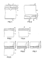
- FIGURE 1 shows a general construction of a V-channeled substrate inner stripe (VSIS) semiconductor laser.
- An n-GaAs current blocking layer 2 is first formed on a p-GaAs substrate 1.
- a V-shaped groove 9, which functions as a current path, is formed in the n-GaAs current blocking layer 2 in a manner to reach the p-GaAs substrate 1.
- a p-GaAlAs cladding layer 3, a GaAlAs active layer 4, an n-GaAlAs cladding layer 5, and an n-GaAs cap layer 6 are formed on the n-GaAs current blocking layer 2 as shown in FIGURE 1.
- n-electrode 7 is formed on the n-GaAs cap layer 6, and a p-electrode 8 is formed on the bottom surface of the p-GaAs substrate 1.
- the current flows only in the stripe region of the V-channel 9, and the beam existing outside of the V-channel 9 is absorbed by the n-GaAs current blocking layer 2.
- the VSIS laser operates at a low threshold current, and exhibits the laser beam of a stable transverse mode. Furthermore, the VSIS laser is suited for the mass production because the fabrication steps thereof do not include the Zn diffusion step nor the pattern alignment step.
- the above-mentioned conventional VSIS laser does not ensure a stable operation when the laser wavelength is shorter than 740 nm. This is because the compressive stress is applied to the GaAlAs active layer 4, which shortens the operating period of the VSIS laser.
- the lattice constant of the GaAs substrate is similar to the lattice constant of the respective grown layers at the growth temperature, about 800 °C.
- the lattice constant of the respective layers and the lattice constant of the GaAs substrate differ from each other at room temperature, because the coefficient of thermal expansion of Ga 1-x Al x As varies as the AlAs mole fraction (x) varies.
- the coefficient of thermal expansion of Ga 1-x Al x As is expressed as follows:
- the difference of the lattice constant creates the stress applied to the active layer 4 at room temperature. If the compressive stress applied to the active layer 4 is minimized, the operating life period of the VSIS laser may be lengthened.
- the GaAs substrate 1, which creates the above-mentioned compressive stress is removed through the use of an etching method. Instead, a cap layer having a desired AlAs mole fraction is formed to a thickness of 100 ⁇ m to support the laser device.
- FIGURE 2 shows an embodiment of a V-channeled substrate inner stripe (VSIS) semiconductor laser of the present invention.
- VSIS V-channeled substrate inner stripe
- the VSIS laser of the present invention includes a p-GaAs layer 21, an n-GaAs current blocking layer 12, a p-GaAlAs cladding layer 13, a GaAlAs active layer 14, and an n-GaAlAs cladding layer 15.
- the p-GaAlAs cladding layer 13 and the n-GaAlAs cladding layer 15 define the active layer 14 by the hetero junctions formed between the active layer 14.
- An n-GaAlAs cap layer 16 is formed on the n-GaAlAs cladding layer 15 in order to achieve the ohmic contact.
- An n-electrode 17 is formed on the n-GaAlAs cap layer 16, and a p-electrode * 18 is formed on the bottom surface of the p-GaAs layer 21 in order to apply the driving current to the GaAlAs active layer 14.
- a V-shaped groove (V-channel) 19 is formed in the n-GaAs current blocking layer 12.
- the p-GaAs layer 21, the n-GaAs current blocking layer 12, the p-GaAlAs cladding layer 13, the GaAlAs active layer 14, the n-GaAlAs cladding layer 15 and the n-GaAlAs cap layer 16 are formed through the use of an epitaxial method.
- the n-GaAlAs cap layer 16 has a thickness sufficient to support the semiconductor laser device.
- FIGURES 3 through 7 show the fabrication steps of the VSIS laser of FIGURE 2.
- a GaAs substrate 11 is provided.
- An etching stop layer 20 (Ga 0.5 Al 0.5 As layer of 1 ⁇ m thick) is formed on the GaAs substrate 11 as shown in FIGURE 3.
- the p-GaAs layer 21 of 2.0 ⁇ m thick, and the n-GaAs current blocking layer 12 of 0.6 ⁇ m thick are formed on the etching stop layer 20.
- the GaAs substrate 11 and the etching stop layer 20 will be removed by the end of the formation of the VSIS laser of the present invention and, therefore, the conductivity thereof is freely selected among the p-type, the n-type, and the undoped.
- the GaAs substrate 11 has, preferably, a low dislocation density.
- a V-shaped groove is formed in the n-GaAs current blocking layer 12 in the ⁇ 110 > direction to reach the p-GaAs layer 21 as shown in FIGURE 4, thereby forming the V-channel 19.
- the p-Ga 0.3 Al 0.7 As cladding layer 13 of 0.1 ⁇ m thick, the p-Ga 0.7 Al 0.3 As active layer 14 of 0.1 ⁇ m thick, the n-Ga 0.3 Al 0.7 As cladding layer 15 of 1.0 pm, and the n-Ga 0.85 Al 0.15 As cap layer 16 of 100 ⁇ m thick are formed on the n-GaAs current blocking layer 12 as shown in FIGURE 5 through the use of the epitaxial method.
- the etchant forms an oxide film on the GaAlAs layer so as to stop the etching operation at the Ga 0.5 Al 0.5 As etching stop layer 20.
- the etching stop layer 20 is removed as shown in FIGURE 7 through the use of an etchant made of hydrofluoric acid. That is, the GaAs substrate 11 and the etching stop layer 20 are completely removed before depositing the electrodes.
- An electrode layer is formed on the n-Ga 0.85 Al 0.15 As cap layer 16 by evaporating Au-Ge-Ni.
- Another electrode layer is formed on the bottom surface of the p-GaAs - layer 21 by evaporating Au-Zn.
- the thus formed electrode layers are alloyed by the thermal treatment, thereby forming the n-electrode 17 and the p-electrode 18, respectively.
- the thus constructed VSIS semiconductor laser exhibits the laser oscillation of the wavelength 690 nm at room temperature with the threshold current of 70 mA.
- the VSIS semiconductor laser of the present invention enjoys an operating life longer than 1000 hours under an output power of 3 mW.
- the present invention is applicable to other semiconductor laser of the three-component system or the four-component system which employs an InP substrate, a GaP substrate or an InAs substrate as the growing substrate.
- the etching stop layer 20 is employed to facilitate the etching operation. However, it may be possible to omit the etching stop layer 20 if the etching operation of the GaAs substrate 11 is properly controlled to reduce the thickness of the GaAs substrate from about 350 microns to several microns.
Landscapes
- Physics & Mathematics (AREA)
- Geometry (AREA)
- Condensed Matter Physics & Semiconductors (AREA)
- General Physics & Mathematics (AREA)
- Electromagnetism (AREA)
- Optics & Photonics (AREA)
- Semiconductor Lasers (AREA)
- Liquid Deposition Of Substances Of Which Semiconductor Devices Are Composed (AREA)
Applications Claiming Priority (2)
| Application Number | Priority Date | Filing Date | Title |
|---|---|---|---|
| JP57089249A JPS58206184A (ja) | 1982-05-25 | 1982-05-25 | 半導体レ−ザ素子及びその製造方法 |
| JP89249/82 | 1982-05-25 |
Publications (3)
| Publication Number | Publication Date |
|---|---|
| EP0095895A2 true EP0095895A2 (fr) | 1983-12-07 |
| EP0095895A3 EP0095895A3 (en) | 1985-05-15 |
| EP0095895B1 EP0095895B1 (fr) | 1988-08-03 |
Family
ID=13965479
Family Applications (1)
| Application Number | Title | Priority Date | Filing Date |
|---|---|---|---|
| EP83303029A Expired EP0095895B1 (fr) | 1982-05-25 | 1983-05-25 | Laser à semi-conducteur |
Country Status (4)
| Country | Link |
|---|---|
| US (1) | US4592062A (fr) |
| EP (1) | EP0095895B1 (fr) |
| JP (1) | JPS58206184A (fr) |
| DE (1) | DE3377606D1 (fr) |
Cited By (3)
| Publication number | Priority date | Publication date | Assignee | Title |
|---|---|---|---|---|
| EP0205338A3 (en) * | 1985-06-11 | 1988-01-20 | Sharp Kabushiki Kaisha | Semiconductor laser device |
| DE3905480A1 (de) * | 1988-02-26 | 1989-08-31 | Mitsubishi Electric Corp | Halbleiterlaser und verfahren zu seiner herstellung |
| GB2287124A (en) * | 1994-02-22 | 1995-09-06 | Mitsubishi Electric Corp | Semiconductor laser and method of fabrication |
Families Citing this family (2)
| Publication number | Priority date | Publication date | Assignee | Title |
|---|---|---|---|---|
| JPS6031288A (ja) * | 1983-07-29 | 1985-02-18 | Sharp Corp | 半導体レ−ザ素子 |
| JPS63258090A (ja) * | 1987-04-15 | 1988-10-25 | Sharp Corp | 半導体レ−ザ装置 |
Family Cites Families (1)
| Publication number | Priority date | Publication date | Assignee | Title |
|---|---|---|---|---|
| JPS5645093A (en) * | 1979-09-20 | 1981-04-24 | Sharp Corp | Manufacturing of semiconductor laser element |
-
1982
- 1982-05-25 JP JP57089249A patent/JPS58206184A/ja active Granted
-
1983
- 1983-05-25 EP EP83303029A patent/EP0095895B1/fr not_active Expired
- 1983-05-25 US US06/498,041 patent/US4592062A/en not_active Expired - Lifetime
- 1983-05-25 DE DE8383303029T patent/DE3377606D1/de not_active Expired
Non-Patent Citations (4)
| Title |
|---|
| APPLIED PHYSICS LETTERS, vol. 36, no. 8, April 1980, pages 634-636, American Institute of Physics, New York, US; CHUNG-YIH CHEN et al.: "Narrow double-current-confinement channeled-substrate planar laser fabricated by double etching technique" * |
| APPLIED PHYSICS LETTERS, vol. 40, no. 5, March 1982, pages 372-374, American Institute of Physics, New York, US; S. YAMAMOTO et al.: "Visible GaAlAs V-channeled substrate inner stripe laser with stabilized mode using p-GaAs substrate" * |
| APPLIED PHYSICS LETTERS, vol. 41, no. 9, 1st November 1982, pages 796-798, American Institute of Physics, New York, US; S. YAMAMOTO et al.: "Room-temperature cw operation in the visible spectral range of 680-700nm by AlGaAs double heterojunction lasers" * |
| IEEE JOURNAL OF QUANTUM ELECTRONICS, vol. QE-17, no. 5, May 1981, pages 763-767, IEEE, New York, US; H. SHIMIZU et al.: "Improvement in operation lives of GaAlAs visible lasers by introducing GaAlAs buffer layers" * |
Cited By (8)
| Publication number | Priority date | Publication date | Assignee | Title |
|---|---|---|---|---|
| EP0205338A3 (en) * | 1985-06-11 | 1988-01-20 | Sharp Kabushiki Kaisha | Semiconductor laser device |
| US4819244A (en) * | 1985-06-11 | 1989-04-04 | Sharp Kabushiki Kaisha | Semiconductor laser device |
| DE3905480A1 (de) * | 1988-02-26 | 1989-08-31 | Mitsubishi Electric Corp | Halbleiterlaser und verfahren zu seiner herstellung |
| US4951289A (en) * | 1988-02-26 | 1990-08-21 | Mitsubishi Denki Kabushiki Kaisha | Semiconductor laser |
| US5028562A (en) * | 1988-02-26 | 1991-07-02 | Mitsubishi Denki Kabushiki Kaisha | Method for producing a semiconductor laser using selective epitaxy |
| GB2287124A (en) * | 1994-02-22 | 1995-09-06 | Mitsubishi Electric Corp | Semiconductor laser and method of fabrication |
| US5541950A (en) * | 1994-02-22 | 1996-07-30 | Mitsubishi Denki Kabushiki Kaisha | Semiconductor laser including groove having variable dimensions |
| GB2287124B (en) * | 1994-02-22 | 1998-01-28 | Mitsubishi Electric Corp | Semiconductor laser and method for fabricating semiconductor laser |
Also Published As
| Publication number | Publication date |
|---|---|
| EP0095895A3 (en) | 1985-05-15 |
| JPS58206184A (ja) | 1983-12-01 |
| US4592062A (en) | 1986-05-27 |
| JPH0416033B2 (fr) | 1992-03-19 |
| EP0095895B1 (fr) | 1988-08-03 |
| DE3377606D1 (en) | 1988-09-08 |
Similar Documents
| Publication | Publication Date | Title |
|---|---|---|
| EP0132081B1 (fr) | Laser à semi-conducteur | |
| EP0373933B1 (fr) | Méthode de production d'un laser à semi-conducteur muni d'une structure non absorbante à miroir | |
| US4188244A (en) | Method of making a semiconductor light-emitting device utilizing low-temperature vapor-phase deposition | |
| KR940005764B1 (ko) | 레이저 다이오드 어레이 및 그 제조방법 | |
| US4716125A (en) | Method of producing semiconductor laser | |
| US4149175A (en) | Solidstate light-emitting device | |
| EP0264225B1 (fr) | Dispositif laser à semi-conducteur et sa méthode de fabrication | |
| US5394421A (en) | Semiconductor laser device including a step electrode in a form of eaves | |
| EP0095895B1 (fr) | Laser à semi-conducteur | |
| EP0321294B1 (fr) | Dispositif laser à semi-conducteur | |
| JPH05218586A (ja) | 半導体レーザ装置およびその製造方法 | |
| EP0160490B1 (fr) | Laser à semi-conducteur | |
| CA1065461A (fr) | Dispositif electrolumininescent a semiconducteurs et methode de fabrication | |
| EP0205338B1 (fr) | Dispositif laser à semi-conducteur | |
| US4841535A (en) | Semiconductor laser device | |
| US5298456A (en) | Method of manufacturing semiconductor laser | |
| EP0124051A2 (fr) | Laser à semi-conducteur | |
| JPH05218585A (ja) | 半導体発光装置 | |
| JP2528877B2 (ja) | 半導体レ−ザ | |
| JPH0682886B2 (ja) | 半導体レーザ装置の製造方法 | |
| JPS61253882A (ja) | 半導体レ−ザ装置 | |
| KR100647293B1 (ko) | 굴절률 도파형 반도체 레이저 다이오드 및 그 제조 방법 | |
| JPH0770779B2 (ja) | 半導体レーザの製造方法 | |
| JP2547459B2 (ja) | 半導体レーザ素子及びその製造方法 | |
| JPH0559594B2 (fr) |
Legal Events
| Date | Code | Title | Description |
|---|---|---|---|
| PUAI | Public reference made under article 153(3) epc to a published international application that has entered the european phase |
Free format text: ORIGINAL CODE: 0009012 |
|
| AK | Designated contracting states |
Designated state(s): DE GB NL |
|
| PUAL | Search report despatched |
Free format text: ORIGINAL CODE: 0009013 |
|
| AK | Designated contracting states |
Designated state(s): DE GB NL |
|
| 17P | Request for examination filed |
Effective date: 19851021 |
|
| 17Q | First examination report despatched |
Effective date: 19861013 |
|
| GRAA | (expected) grant |
Free format text: ORIGINAL CODE: 0009210 |
|
| AK | Designated contracting states |
Kind code of ref document: B1 Designated state(s): DE GB NL |
|
| REF | Corresponds to: |
Ref document number: 3377606 Country of ref document: DE Date of ref document: 19880908 |
|
| PLBE | No opposition filed within time limit |
Free format text: ORIGINAL CODE: 0009261 |
|
| STAA | Information on the status of an ep patent application or granted ep patent |
Free format text: STATUS: NO OPPOSITION FILED WITHIN TIME LIMIT |
|
| 26N | No opposition filed | ||
| REG | Reference to a national code |
Ref country code: GB Ref legal event code: IF02 |
|
| PGFP | Annual fee paid to national office [announced via postgrant information from national office to epo] |
Ref country code: GB Payment date: 20020522 Year of fee payment: 20 |
|
| PGFP | Annual fee paid to national office [announced via postgrant information from national office to epo] |
Ref country code: NL Payment date: 20020529 Year of fee payment: 20 Ref country code: DE Payment date: 20020529 Year of fee payment: 20 |
|
| PG25 | Lapsed in a contracting state [announced via postgrant information from national office to epo] |
Ref country code: GB Free format text: LAPSE BECAUSE OF EXPIRATION OF PROTECTION Effective date: 20030524 |
|
| PG25 | Lapsed in a contracting state [announced via postgrant information from national office to epo] |
Ref country code: NL Free format text: LAPSE BECAUSE OF EXPIRATION OF PROTECTION Effective date: 20030525 |
|
| REG | Reference to a national code |
Ref country code: GB Ref legal event code: PE20 |
|
| NLV7 | Nl: ceased due to reaching the maximum lifetime of a patent |
Effective date: 20030525 |