EP0096341B1 - Système optique d'une imprimante laser - Google Patents
Système optique d'une imprimante laser Download PDFInfo
- Publication number
- EP0096341B1 EP0096341B1 EP83105386A EP83105386A EP0096341B1 EP 0096341 B1 EP0096341 B1 EP 0096341B1 EP 83105386 A EP83105386 A EP 83105386A EP 83105386 A EP83105386 A EP 83105386A EP 0096341 B1 EP0096341 B1 EP 0096341B1
- Authority
- EP
- European Patent Office
- Prior art keywords
- digital
- signal
- output signal
- laser
- laser diode
- Prior art date
- Legal status (The legal status is an assumption and is not a legal conclusion. Google has not performed a legal analysis and makes no representation as to the accuracy of the status listed.)
- Expired
Links
- 230000003287 optical effect Effects 0.000 title claims description 16
- 238000001514 detection method Methods 0.000 claims description 27
- 238000012423 maintenance Methods 0.000 claims description 7
- 238000005070 sampling Methods 0.000 description 8
- 238000006243 chemical reaction Methods 0.000 description 5
- 230000015654 memory Effects 0.000 description 5
- 230000015556 catabolic process Effects 0.000 description 4
- 238000006731 degradation reaction Methods 0.000 description 4
- 238000010586 diagram Methods 0.000 description 4
- 238000000034 method Methods 0.000 description 3
- 230000004044 response Effects 0.000 description 3
- 230000001360 synchronised effect Effects 0.000 description 2
- 230000002238 attenuated effect Effects 0.000 description 1
- 239000003990 capacitor Substances 0.000 description 1
- 238000004140 cleaning Methods 0.000 description 1
- 238000010276 construction Methods 0.000 description 1
- 230000007423 decrease Effects 0.000 description 1
- 230000003247 decreasing effect Effects 0.000 description 1
- 230000001419 dependent effect Effects 0.000 description 1
- 230000000694 effects Effects 0.000 description 1
- 230000001960 triggered effect Effects 0.000 description 1
Images

Classifications
-
- H—ELECTRICITY
- H01—ELECTRIC ELEMENTS
- H01S—DEVICES USING THE PROCESS OF LIGHT AMPLIFICATION BY STIMULATED EMISSION OF RADIATION [LASER] TO AMPLIFY OR GENERATE LIGHT; DEVICES USING STIMULATED EMISSION OF ELECTROMAGNETIC RADIATION IN WAVE RANGES OTHER THAN OPTICAL
- H01S5/00—Semiconductor lasers
- H01S5/06—Arrangements for controlling the laser output parameters, e.g. by operating on the active medium
- H01S5/068—Stabilisation of laser output parameters
- H01S5/0683—Stabilisation of laser output parameters by monitoring the optical output parameters
Definitions
- the present invention relates to a laser printer optical system, of the kind referred to in the precharacterizing portion of patent claim 1.
- a laser printer optical system is known from DE-A-31 02 185.
- a photoconductive surface of a drum is scanned by and exposed to laser light emitted from the laser diode to form an electrostatic latent image in the photoconductive surface, and then a toner image obtained by developing the latent image of electric charge is transferred to ordinary recording paper to fix the transferred toner image, thereby recording a desired image on the recording paper.
- laser light is modulated by a video signal for forming a picture image, in such a manner that a laser-diode driving current is fed or cut in accordance with the video signal, that is, the laser light is intermittently generated.
- the scanning exposure of the photoconductive surface of the drum is carried out in the following manner.
- the photoconductive surface of the drum is repeatedly scanned with a laser light spot in a direction parallel to the rotating axis of the drum by deflecting the laser light by means of a rotating mirror or vibrating mirror, while rotating the drum at a constant speed.
- the laser light is deflected to the outside of a picture image area on the photoconductive surface of the drum, and the deflected light impinges upon a photoelectric conversion element which is disposed on the outside of the above-mentioned area for the purpose of position detection.
- a deflecting position can be detected.
- the photoelectric transducer for position detection is generally disposed on the side of the starting point of a scanning line, and the laser light is modulated in accordance with the time elapsed after the laser light spot has left the photoelectric transducer. Further, in order to cause the laser light emitted from the laser diode to form the laser light spot having a predetermined shape on the photoconductive surface of the drum. to prevent the laser light spot from deviating from the scanning position, or to prevent a deflecting angle of the laser light formed by a deflecting mirror from being too large, various lenses and mirrors are arranged on a laser light path.
- the intensity of laser light incident upon the photoconductive surface of the drum is required to be kept on a predetermined constant level, in order to obtain a picture image of high quality. Since the luminous intensity of a laser diode varies with temperature, it has been proposed to provide in the laser beam printers thermostatic means for maintaining the laser diode at a constant temperature. However, the luminous efficiency of the laser diode also decreases due to the fatique or degradation thereof. Further, in the laser beam printers, laser light incident upon the photoconductive surface of the drum is attenuated by stains on the lenses and mirrors, and therefore the intensity of the laser light incident upon the photoconductive surface varies even when the laser diode is kept at a constant temperature.
- a laser printer optical system including a light receiving drum and a light source
- a control circuit for controlling a current supplied to a laser diode emitting a beam which is scanned into the drum
- said control circuit comprising: a photoelectric transducer for converting the intensity of laser light emitted from said laser diode into an analog detection signal; a comparator for comparing said analog detection signal with a reference electrical signal to deliver a binary signal; a digital up;down counter applied with said binary signal to change over from one of an up-count mode and a down-count mode to the other; a digital-to-analog converter for converting a digital output signal from said digital up;down counter into an analog output signal; and a current control circuit for controlling a current flowing through said laser diode, in accordance with said analog output signal.
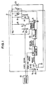
- Fig. 1 is a block diagram showing the whole construction of an embodiment of a laser printer optical system according to the present invention:
- Fig. 2 is a block diagram showing in detail a portion of the embodiment shown in Fig. 1.
- the intensity of laser light emitted from a laser diode varies with a current flowing through the laser diode.
- an output from output means is detected to be compared with a reference value, and an input to the output means is corrected on the basis of a difference between the output and reference value.
- laser light is intermittently generated due to intensity modulation and deflected so as to scan a predetermined area. Accordingly, it is required to detect the intensity of the laser light in a short time by a photoelectric detector, and to hold the detected value till the next detecting time.
- an analog memory circuit for sampling/holding an analog detection signal delivered from a photoelectric transducer for light-intensity detection and a digital memory circuit for storing therein a digital signal obtained by subjecting the analog detection signal to analog-to-digital conversion.
- the time in which the intensity of laser light is detected is very short. Accordingly, the analog memory dircuit and digital memory circuit are required to be rapid in response, and therefore they are expensive.
- the analog detection signal indicating a photoelectric conversion value of laser light is not obtained, or in the case where the moment the analog detection signal is generated, is not synchronized with the moment the analog detection signal is sampled, the value to be stored in each of the memories becomes zero, and therefore the difference between the detected value and a reference value becomes large.
- the current flowing through the laser diode is corrected on the basis of such a large difference, an excessive current flows through the laser diode. and thus the life thereof is shortened.
- the feed-back control used in the present invention it is judged by a comparator only whether the analog detection signal indicating a photoelectric conversion value of laser light is greater than a reference value or not, that is, the difference value between the analog detection signal and reference value is not taken into consideration, and a digital up down counter counts a clock signal which is applied to the counter when a binary signal such as a high or low level signal which is delivered from the comparator. Accordingly, the present invention can employ circuit elements which are inexpensive and rapid in response. Further, even when the difference between the analog detection signal and reference value is large. a large correction current does not flow through the laser diode, and therefore the life thereof is not shortened.
- the number of clock pulses which are supplied to the up down counter when the binary signal is delivered from the comparator can be made small (for example, made equal to one).
- Fig. 1 shows, in a block diagram. a control circuit included in an embodiment of the present invention.
- a current flowing through a laser diode 1 is controlled by a current control circuit 2.
- the circuit 2 includes transistors 3 and 4 making up a differential switch, and a constant current source 5.
- the emitters of the transistors 3 and 4 are connected to a constant current source 5 in common.
- the collector of the transistor 3 is connected to a power line through a resistor 6, and the collector of the transistor 4 is connected to the power line through a parallel combination of the laser diode 1, a reverse-voltage protecting diode 7 and a resistor 8.
- Resistors 9 and 10 are used for applying a bias voltage to the transistor 3, and resistors 11 and 12 are used for applying a bias voltage to the transistor 4.
- a photodiode 13 for photoelectric conversion is placed at a scanning position of deflected laser light, and delivers an analog detection signal corresponding to the intensity of laser light emitted from the laser diode 1. It is judged by a comparator 16 whether the analog detection signal delivered from the photodiode 13 is greater than a reference electrical signal determined by voltage- dividing resistors 14 and 15 or not. A binary signal delivered from the comparator 16 takes a high level when the analog detection signal is smaller than the reference electrical signal, and takes a low level when the analog detection signal is greater than the reference electrical signal.
- a digital up down counter (hereinafter referred to as a "U D counter”) 17 takes an up-count mode or a down-count mode according as the binary signal applied to a count-mode control terminal U D takes the high or low level, to count a sampling clock signal which is supplied from a signal generator 18 to a clock terminal CK.
- a digital output signal delivered from the U D counter 17 is converted into an analog output signal by a digital-to-analog converter (hereinafter referred to as a "D A converter”) 19.
- the constant current source 5 is controlled by the analog output signal. and thus a constant current is set in accordance with the analog output signal.
- a video signal delivered from the signal generator 18 is applied to the base of the transistor 3.
- Fig. 2 is a block diagram showing in detail a circuit portion including the U D counter 17 and D A converter 19.
- the U D counter 17 includes 4-bit U D counters 17a and 17b to form an 8-bit U D counter.
- An 8-bit digital output signal from the U D counter 17 is applied to input terminals of each of the 8-bit D A converter 19 and an 8-input NAND gate 17c.
- Count-mode control terminals (hereinafter referred to as "U D terminals") 5 and of the U D counters 17a and 17b are connected to the output terminal of a 2-input AND gate 17d.
- Data input terminals to and 6 to 9 and to of the counters 17a and 17b are grounded to take a low level Load input termmals 10 and of the counters 17a and 17b are connected to an initializing circuit made up of a diode 17e, a resistor 17f and a capacitor 17g, to be applied with a load pulse when a power switch (not shown) is turned on.
- the 2-input AND gate 17d is applied with the binary signal delivered from the comparator 16 and the output signal of the 8-input NAND gate 17c.
- the output signal of the 8-input NAND gate 17c also triggers a flip-flop circuit 17h to generate a maintenance signal, which operates an indicator 20.
- the analog output signal from the D/A converter 19 is applied to the constant current source 5.
- the analog detection signal from the photodiode 13 is small in amplitude. That is, the analog detection signal is smaller than the reference electrical signal which is to be compared with the analog detection signal by the comparator 16. Accordingly, the binary signal delivered from the comparator 16 takes a high level. Further, the output signal of the 8-input NAND gate 17c takes a high level. Therefore, the output signal of the 2- input AND gate 17d takes a high level. Thus, the U.
- D counters 17a and 17b take the up-count mode, and therefore count up by one least significant bit (namely, one LSB) of the input applied to the D A converter 19, each time the sampling signal is applied to the counters 17a and 17b.
- the U D counters 17a and 17b count up to make large the digital output signal, and therefore the analog output signal from the D,A converter 19 becomes large, thereby increasing the set current in the constant current source 5.
- the binary signal delivered from the comparator 16 takes a low level.
- the U D counters 17a and 17b take the down-count mode, and therefore count down by one LSB of the input applied to the D/A converter 19, each time the sampling clock signal is applied to the counters 17a and 17b. That is, the digital output signal from the counters 17a and 17b becomes small, and therefore the analog output signal from the D/A converter 19 also becomes small.
- the set current in the constant current source 5 is reduced.
- the analog detection signal delivered from the photodiode 13 is made smaller than the reference electrical signal.
- the binary signal from the comparator 16 takes the high level, and thus the UiD counters 17a and 17b take the up-count mode to increase the set current in the constant current source 5.
- a current for driving the laser diode 1 is controlled so that the intensity of laser light emitted from the laser diode 1 lies in a range corresponding to a variation of ⁇ 1 LSB about a predetermined value.
- the current control operation is performed in the state that the contents of the U/D counters 17a and 17b have been increased by the above-mentioned one LSB.
- the operating point of the U D counters 17a and 17b becomes higher as the fatigue or degradation of the laser diode 1 proceeds or the stain in the optical system becomes large.
- the digital output signal takes a value "FF" (namely, a maximum value of the contents of the U D counters 17a and 17b).
- the circuit characteristic of the above-mentioned circuit configuration is previously set so that the digital output signal takes the value "FF" at the same time as the current for driving the laser diode 1 takes a maximum permissible value.
- the digital output signal takes the value "FF”
- all input terminals of the 8-input NAND gate 17c are kept at a high level, and the output signal of the gate 17c takes a low level.
- the 2-input AND gate 17d takes a low level, and the U D counters 17a and 17b take the down-count mode.
- the next sampling signal is supplied to the U D counters 17a and 17b.
- the digital output signal from the U D counters takes a value "FE” (namely, a value next to the previously-mentioned maximum value "FF").
- the output signal of the 8-input NAND gate 17c again takes the high level, to cause the U D counters 17a and 17b to take the up-count mode.
- the current control operation is performed in a range defined by the values "FF" and "FE". in order to prevent the current for driving the laser diode 1 from exceeding the maximum permissible value.
- the flip-flop circuit 17h is triggered by the low-level signal from the NAND gate 17c to generate the maintenance signal, which operates the indicator 20.
- the generation of laser light is modulated by a video signal sent out from the signal generator 18, to form a picture image.
- the video signal takes a high level
- the transistor 3 is turned on and the transistor 4 is turned off.
- the laser diode 1 does not emit laser light (or emits a weak laser beam substantially incapable of producing an exposure effect on the photoconductive surface of the drum).
- the video signal takes a low level
- the transistor 3 is turned off and the transistor 4 is turned on.
- the laser diode is operated at a current set by the above-mentioned current control operation, and thus emits laser light having a predetermined intensity.
- the present embodiment has the following advantages.
- a laser printer optical system in which the intensity of laser light on a predetermined laser light path is kept constant.
Landscapes
- Physics & Mathematics (AREA)
- Condensed Matter Physics & Semiconductors (AREA)
- General Physics & Mathematics (AREA)
- Electromagnetism (AREA)
- Optics & Photonics (AREA)
- Semiconductor Lasers (AREA)
- Laser Beam Printer (AREA)
- Dot-Matrix Printers And Others (AREA)
- Exposure Or Original Feeding In Electrophotography (AREA)
- Facsimile Scanning Arrangements (AREA)
- Control Of Non-Electrical Variables (AREA)
Claims (4)
Applications Claiming Priority (2)
| Application Number | Priority Date | Filing Date | Title |
|---|---|---|---|
| JP93973/82 | 1982-06-03 | ||
| JP57093973A JPS58212256A (ja) | 1982-06-03 | 1982-06-03 | レ−ザ光源装置 |
Publications (3)
| Publication Number | Publication Date |
|---|---|
| EP0096341A2 EP0096341A2 (fr) | 1983-12-21 |
| EP0096341A3 EP0096341A3 (en) | 1987-04-01 |
| EP0096341B1 true EP0096341B1 (fr) | 1991-03-20 |
Family
ID=14097341
Family Applications (1)
| Application Number | Title | Priority Date | Filing Date |
|---|---|---|---|
| EP83105386A Expired EP0096341B1 (fr) | 1982-06-03 | 1983-05-31 | Système optique d'une imprimante laser |
Country Status (4)
| Country | Link |
|---|---|
| US (1) | US4580044A (fr) |
| EP (1) | EP0096341B1 (fr) |
| JP (1) | JPS58212256A (fr) |
| DE (1) | DE3382217D1 (fr) |
Families Citing this family (40)
| Publication number | Priority date | Publication date | Assignee | Title |
|---|---|---|---|---|
| JPS61165835A (ja) * | 1985-01-17 | 1986-07-26 | Olympus Optical Co Ltd | 光出力安定化装置 |
| JPS61165836A (ja) * | 1985-01-17 | 1986-07-26 | Olympus Optical Co Ltd | 光出力安定化装置 |
| US4856011A (en) * | 1985-01-30 | 1989-08-08 | Ricoh Company, Ltd. | Semiconductor laser control circuit |
| US4763334A (en) * | 1985-01-30 | 1988-08-09 | Ricoh Company, Ltd. | Laser beam emitting apparatus |
| JP2539358B2 (ja) * | 1985-03-20 | 1996-10-02 | オリンパス光学工業株式会社 | 光学式記録再生装置における半導体レ―ザ劣化判別装置 |
| JP2644721B2 (ja) * | 1985-03-29 | 1997-08-25 | キヤノン株式会社 | レーザユニット |
| US4985896A (en) * | 1985-03-29 | 1991-01-15 | Canon Kabushiki Kaisha | Laser driving device |
| JP2644722B2 (ja) * | 1985-03-29 | 1997-08-25 | キヤノン株式会社 | 画像形成装置 |
| JPS61224476A (ja) * | 1985-03-29 | 1986-10-06 | Canon Inc | レ−ザ電流制限装置 |
| JPS62116570U (fr) * | 1986-01-16 | 1987-07-24 | ||
| US4937799A (en) * | 1985-12-13 | 1990-06-26 | Canon Kabushiki Kaisha | Method and apparatus for setting light quantity most suitable for reproducing information from an optical recording medium |
| US4718118A (en) * | 1986-02-24 | 1988-01-05 | Rca Corporation | Transparent laser drive current update for burst mode fiber optic communication system |
| US4730105A (en) * | 1986-07-25 | 1988-03-08 | American Telephone And Telegraph Company, At&T Bell Laboratories | Apparatus for the stabilization of the output intensity of a laser using a Fabry-Perot cavity |
| US4890288A (en) * | 1986-08-27 | 1989-12-26 | Canon Kabushiki Kaisha | Light quantity control device |
| US4740686A (en) * | 1986-09-09 | 1988-04-26 | The Perkin-Elmer Corporation | Optical sensor circuitry |
| JPH0614663B2 (ja) * | 1986-09-19 | 1994-02-23 | 株式会社リコー | 光走査装置 |
| JPS63193582A (ja) * | 1987-02-06 | 1988-08-10 | Ando Electric Co Ltd | レ−ザダイオ−ド駆動回路 |
| EP0497431B1 (fr) * | 1987-04-13 | 1995-06-28 | Sharp Kabushiki Kaisha | Appareil pour commander un dispositif à laser à semi-conducteur |
| JP2611220B2 (ja) * | 1987-04-15 | 1997-05-21 | ソニー株式会社 | レーザ再生装置 |
| DE3726244C2 (de) * | 1987-08-07 | 1993-11-18 | Kommunikations Elektronik | Schaltungsanordnung zur Überwachung der Leistung einer Laserdiode |
| US4803497A (en) * | 1987-08-31 | 1989-02-07 | Dr.-Ing. Rudolf Hell Gmbh | Laser diode output power stabilization in a laser imagesetter |
| JPH0296936A (ja) * | 1988-06-01 | 1990-04-09 | Canon Inc | レーザダイオード駆動回路 |
| US5067117A (en) * | 1988-10-28 | 1991-11-19 | Fuji Electric Co., Ltd. | Output stabilizing apparatus for an optical head |
| US5017944A (en) * | 1989-03-06 | 1991-05-21 | Victor Company Of Japan, Ltd. | Control system for information recording laser beam |
| DE3940720A1 (de) * | 1989-12-09 | 1991-06-13 | Bosch Gmbh Robert | Schaltungsanordnung zum betrieb einer lichtquelle fuer die optische abtastung von aufzeichnungstraegern |
| US5248879A (en) * | 1992-10-19 | 1993-09-28 | Ncr Corporation | Circuit for adjusting the sensitivity of a sensor using a digital counter and a low-pass filter |
| US5502298A (en) * | 1992-12-21 | 1996-03-26 | Ericsson Raynet | Apparatus and method for controlling an extinction ratio of a laser diode over temperature |
| JPH09148630A (ja) * | 1995-11-21 | 1997-06-06 | Rohm Co Ltd | 光量調整回路及びこれを用いた光応用装置 |
| US5953690A (en) * | 1996-07-01 | 1999-09-14 | Pacific Fiberoptics, Inc. | Intelligent fiberoptic receivers and method of operating and manufacturing the same |
| US6201820B1 (en) * | 1997-03-05 | 2001-03-13 | Silkroad, Inc. | Optically modulated laser beam transceiver |
| JP3456120B2 (ja) * | 1997-09-09 | 2003-10-14 | 三菱電機株式会社 | レーザダイオード用電源制御装置 |
| JP3456121B2 (ja) * | 1997-09-09 | 2003-10-14 | 三菱電機株式会社 | レーザダイオード用電源制御装置 |
| DE20007884U1 (de) * | 2000-05-02 | 2001-09-06 | iC-Haus GmbH, 55294 Bodenheim | Monolithisch integrierter Schaltkreis zum Regeln der Lichtleistung einer Laserdiode |
| US7079775B2 (en) | 2001-02-05 | 2006-07-18 | Finisar Corporation | Integrated memory mapped controller circuit for fiber optics transceiver |
| TW550555B (en) * | 2001-11-23 | 2003-09-01 | Aopen Inc | Automatic control method for generating stable laser power (ACSP) of a compact disk drive |
| US7215891B1 (en) | 2003-06-06 | 2007-05-08 | Jds Uniphase Corporation | Integrated driving, receiving, controlling, and monitoring for optical transceivers |
| US7408567B2 (en) * | 2005-03-29 | 2008-08-05 | Kabushiki Kaisha Toshiba | Light beam scanning apparatus and image forming apparatus |
| JP4725166B2 (ja) * | 2005-03-31 | 2011-07-13 | ブラザー工業株式会社 | 画像形成装置 |
| JP2009088285A (ja) * | 2007-09-28 | 2009-04-23 | Toshiba Corp | 発光素子駆動回路およびそれを用いた情報記録再生装置 |
| US8159956B2 (en) | 2008-07-01 | 2012-04-17 | Finisar Corporation | Diagnostics for serial communication busses |
Family Cites Families (10)
| Publication number | Priority date | Publication date | Assignee | Title |
|---|---|---|---|---|
| US4133008A (en) * | 1977-03-14 | 1979-01-02 | Rapicom Inc. | Automatic illumination compensation circuit |
| US4097732A (en) * | 1977-06-02 | 1978-06-27 | Burroughs Corporation | Automatic gain control for photosensing devices |
| US4097731A (en) * | 1977-06-02 | 1978-06-27 | Burroughs Corporation | Automatic gain control for photosensing devices |
| JPS548423A (en) * | 1977-06-21 | 1979-01-22 | Canon Inc | Recording device |
| US4158132A (en) * | 1977-07-14 | 1979-06-12 | Electronics Diversified, Inc. | Lighting-control system with cue-level confirmation |
| CA1101923A (fr) * | 1978-09-21 | 1981-05-26 | Joseph Straus | Fonctionnement de laser par injection |
| US4443695A (en) * | 1980-01-25 | 1984-04-17 | Canon Kabushiki Kaisha | Apparatus for controlling the quantity of light |
| JPS56152456U (fr) * | 1980-04-14 | 1981-11-14 | ||
| JPS5713327A (en) * | 1980-06-27 | 1982-01-23 | Laurel Bank Mach Co Ltd | Optical detector |
| JPS57162481A (en) * | 1981-03-23 | 1982-10-06 | Ibm | Control circuit for light emtting semiconductor device |
-
1982
- 1982-06-03 JP JP57093973A patent/JPS58212256A/ja active Granted
-
1983
- 1983-05-31 DE DE8383105386T patent/DE3382217D1/de not_active Expired - Lifetime
- 1983-05-31 EP EP83105386A patent/EP0096341B1/fr not_active Expired
- 1983-06-01 US US06/499,869 patent/US4580044A/en not_active Expired - Lifetime
Also Published As
| Publication number | Publication date |
|---|---|
| US4580044A (en) | 1986-04-01 |
| JPH0414540B2 (fr) | 1992-03-13 |
| EP0096341A3 (en) | 1987-04-01 |
| DE3382217D1 (de) | 1991-04-25 |
| JPS58212256A (ja) | 1983-12-09 |
| EP0096341A2 (fr) | 1983-12-21 |
Similar Documents
| Publication | Publication Date | Title |
|---|---|---|
| US4580044A (en) | Laser apparatus with control circuit for stabilizing laser output | |
| US4890288A (en) | Light quantity control device | |
| JPH0422600Y2 (fr) | ||
| US4967284A (en) | Image forming apparatus and method of controlling output of semiconductor laser | |
| EP0180391B1 (fr) | Amplificateur à balayage de trame | |
| US4807239A (en) | Drive and control circuit for laser diode | |
| US4907236A (en) | Method of controlling the quantity of light in a selected range | |
| US4831247A (en) | Light beam scanning apparatus employing rotating polygon mirror | |
| EP0355839B1 (fr) | Appareil de balayage à rayon optique | |
| JPH05212900A (ja) | 画像形成方法 | |
| US3936756A (en) | Field emission electron gun having automatic current control | |
| JPH0313586B2 (fr) | ||
| JPH0618422B2 (ja) | レーザ記録装置 | |
| US5222072A (en) | Laser power control apparatus | |
| US5416504A (en) | Semiconductor laser control apparatus | |
| JPH0363073B2 (fr) | ||
| JP3728090B2 (ja) | 画像形成装置 | |
| US5140601A (en) | Output control apparatus of laser unit and adjusting method thereof | |
| JPH1083102A (ja) | 光源の異常判定装置及び方法 | |
| JP2000187374A (ja) | 画像形成装置 | |
| JPH09321377A (ja) | 半導体レーザの出射パワー調整方法および装置 | |
| JP3424429B2 (ja) | 光走査装置 | |
| JPH0530314A (ja) | 画像形成装置 | |
| JP2685174B2 (ja) | レーザ記録装置 | |
| JP2733954B2 (ja) | 発光強度制御装置および記録装置 |
Legal Events
| Date | Code | Title | Description |
|---|---|---|---|
| PUAI | Public reference made under article 153(3) epc to a published international application that has entered the european phase |
Free format text: ORIGINAL CODE: 0009012 |
|
| AK | Designated contracting states |
Designated state(s): CH DE FR GB LI NL |
|
| PUAL | Search report despatched |
Free format text: ORIGINAL CODE: 0009013 |
|
| AK | Designated contracting states |
Kind code of ref document: A3 Designated state(s): CH DE FR GB LI NL |
|
| 17P | Request for examination filed |
Effective date: 19870827 |
|
| 17Q | First examination report despatched |
Effective date: 19880415 |
|
| GRAA | (expected) grant |
Free format text: ORIGINAL CODE: 0009210 |
|
| RBV | Designated contracting states (corrected) |
Designated state(s): DE FR GB NL |
|
| AK | Designated contracting states |
Kind code of ref document: B1 Designated state(s): DE FR GB NL |
|
| REF | Corresponds to: |
Ref document number: 3382217 Country of ref document: DE Date of ref document: 19910425 |
|
| ET | Fr: translation filed | ||
| PLBE | No opposition filed within time limit |
Free format text: ORIGINAL CODE: 0009261 |
|
| STAA | Information on the status of an ep patent application or granted ep patent |
Free format text: STATUS: NO OPPOSITION FILED WITHIN TIME LIMIT |
|
| 26N | No opposition filed | ||
| PGFP | Annual fee paid to national office [announced via postgrant information from national office to epo] |
Ref country code: FR Payment date: 19940317 Year of fee payment: 12 |
|
| PGFP | Annual fee paid to national office [announced via postgrant information from national office to epo] |
Ref country code: GB Payment date: 19940520 Year of fee payment: 12 |
|
| PGFP | Annual fee paid to national office [announced via postgrant information from national office to epo] |
Ref country code: NL Payment date: 19940531 Year of fee payment: 12 |
|
| PG25 | Lapsed in a contracting state [announced via postgrant information from national office to epo] |
Ref country code: GB Effective date: 19950531 |
|
| PG25 | Lapsed in a contracting state [announced via postgrant information from national office to epo] |
Ref country code: NL Effective date: 19951201 |
|
| GBPC | Gb: european patent ceased through non-payment of renewal fee |
Effective date: 19950531 |
|
| NLV4 | Nl: lapsed or anulled due to non-payment of the annual fee |
Effective date: 19951201 |
|
| PG25 | Lapsed in a contracting state [announced via postgrant information from national office to epo] |
Ref country code: FR Effective date: 19960229 |
|
| REG | Reference to a national code |
Ref country code: FR Ref legal event code: ST |
|
| REG | Reference to a national code |
Ref country code: FR Ref legal event code: ST |
|
| PGFP | Annual fee paid to national office [announced via postgrant information from national office to epo] |
Ref country code: DE Payment date: 20020628 Year of fee payment: 20 |