EP0096369A2 - Unité fonctionnelle de mémoire - Google Patents
Unité fonctionnelle de mémoire Download PDFInfo
- Publication number
- EP0096369A2 EP0096369A2 EP83105462A EP83105462A EP0096369A2 EP 0096369 A2 EP0096369 A2 EP 0096369A2 EP 83105462 A EP83105462 A EP 83105462A EP 83105462 A EP83105462 A EP 83105462A EP 0096369 A2 EP0096369 A2 EP 0096369A2
- Authority
- EP
- European Patent Office
- Prior art keywords
- columns
- rows
- redundant
- cell field
- cell array
- Prior art date
- Legal status (The legal status is an assumption and is not a legal conclusion. Google has not performed a legal analysis and makes no representation as to the accuracy of the status listed.)
- Granted
Links
- 238000012360 testing method Methods 0.000 abstract description 22
- 238000012876 topography Methods 0.000 abstract description 4
- 238000004519 manufacturing process Methods 0.000 description 2
- 241001136792 Alle Species 0.000 description 1
- 101100310222 Caenorhabditis briggsae she-1 gene Proteins 0.000 description 1
- 230000002950 deficient Effects 0.000 description 1
- 230000001419 dependent effect Effects 0.000 description 1
- 238000005516 engineering process Methods 0.000 description 1
- 230000010354 integration Effects 0.000 description 1
- 230000007257 malfunction Effects 0.000 description 1
- 238000005259 measurement Methods 0.000 description 1
- 238000004377 microelectronic Methods 0.000 description 1
- 230000008672 reprogramming Effects 0.000 description 1
Images
Classifications
-
- G—PHYSICS
- G11—INFORMATION STORAGE
- G11C—STATIC STORES
- G11C29/00—Checking stores for correct operation ; Subsequent repair; Testing stores during standby or offline operation
- G11C29/70—Masking faults in memories by using spares or by reconfiguring
-
- G—PHYSICS
- G11—INFORMATION STORAGE
- G11C—STATIC STORES
- G11C29/00—Checking stores for correct operation ; Subsequent repair; Testing stores during standby or offline operation
- G11C29/04—Detection or location of defective memory elements, e.g. cell constructio details, timing of test signals
- G11C29/08—Functional testing, e.g. testing during refresh, power-on self testing [POST] or distributed testing
- G11C29/12—Built-in arrangements for testing, e.g. built-in self testing [BIST] or interconnection details
- G11C29/18—Address generation devices; Devices for accessing memories, e.g. details of addressing circuits
- G11C29/24—Accessing extra cells, e.g. dummy cells or redundant cells
Definitions
- the invention relates to an integrated memory module with redundant memory rows and / or columns according to the preamble of claim 1.
- the invention is based on the object of designing a memory module with redundant memory elements in such a way that even without knowledge of the replaced rows and / or columns, a complete test with test times which are linearly dependent on the number of memory cells is possible. Solutions to this problem can be found in patent claims 1 and 2.
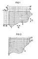
- FIG. 1 shows a section of a cell field M, the rows Z and columns S of which are indicated by intersecting straight lines.
- the marginal row and the marginal column of the cell field M are highlighted by thick lines.
- the rows Z or columns S of the cell field M have the distances d Z and d s from one another. Outside the cell field M, two spare lines RZ and two spare columns RS are indicated by dashed lines.
- the distances d RZ or d RS of the redundant rows or columns from one another and from the outer row or column of the cell field M are significantly larger, preferably approximately twice as large as the corresponding distances d Z and d S of the rows Z or columns S within the cell field M.
- FIG. 2 A further possibility of arranging redundant rows and columns relative to the cell field M with the aim of obtaining short test times is shown in FIG. 2.
- only one replacement row or column ie. H.
- a maximum of two spare rows and two spare columns are provided.
- the further replacement rows and / or replacement columns are moved into the interior of the cell field M such that at least one row or two rows are located between two redundant rows or columns. Column of the cell field M is located.
- FIG. 2 which schematically shows only a section of a cell field M
- two replacement lines RZ1 and RZ2 are provided at an edge of the cell field M.
- the replacement row RZ1 lies outside the cell field M, the outer row Z1 and column S1 are again highlighted by thicker lines.
- the second replacement line RZ2 is located between the outer line Z1 of the cell field M and the line Z2 following inwards.
- a further replacement line might have to be placed between the second and third lines of the cell field M.
- the distances between the replacement rows and the adjacent rows of the cell field or between the replacement columns and the adjacent columns of the cell field can be made larger than the distances otherwise specified in the cell field. This makes it possible to limit the entire test of the module to the first pass specified above without great risk.
Landscapes
- For Increasing The Reliability Of Semiconductor Memories (AREA)
- Techniques For Improving Reliability Of Storages (AREA)
- Tests Of Electronic Circuits (AREA)
- Read Only Memory (AREA)
- Storing Facsimile Image Data (AREA)
Priority Applications (1)
| Application Number | Priority Date | Filing Date | Title |
|---|---|---|---|
| AT83105462T ATE43189T1 (de) | 1982-06-04 | 1983-06-01 | Speicherbaustein. |
Applications Claiming Priority (2)
| Application Number | Priority Date | Filing Date | Title |
|---|---|---|---|
| DE3221268A DE3221268C1 (de) | 1982-06-04 | 1982-06-04 | Speicherbaustein |
| DE3221268 | 1982-06-04 |
Publications (3)
| Publication Number | Publication Date |
|---|---|
| EP0096369A2 true EP0096369A2 (fr) | 1983-12-21 |
| EP0096369A3 EP0096369A3 (en) | 1987-03-04 |
| EP0096369B1 EP0096369B1 (fr) | 1989-05-17 |
Family
ID=6165412
Family Applications (1)
| Application Number | Title | Priority Date | Filing Date |
|---|---|---|---|
| EP83105462A Expired EP0096369B1 (fr) | 1982-06-04 | 1983-06-01 | Unité fonctionnelle de mémoire |
Country Status (5)
| Country | Link |
|---|---|
| US (1) | US4564924A (fr) |
| EP (1) | EP0096369B1 (fr) |
| JP (1) | JPS592289A (fr) |
| AT (1) | ATE43189T1 (fr) |
| DE (2) | DE3221268C1 (fr) |
Families Citing this family (3)
| Publication number | Priority date | Publication date | Assignee | Title |
|---|---|---|---|---|
| JPS62120822A (ja) * | 1985-11-19 | 1987-06-02 | テンパ−ル工業株式会社 | 遠赤外線加熱調理器 |
| JPS62120823A (ja) * | 1985-11-19 | 1987-06-02 | テンパ−ル工業株式会社 | 遠赤外線加熱調理器 |
| DE69032844T2 (de) * | 1989-01-31 | 1999-05-12 | Fujitsu Ltd., Kawasaki, Kanagawa | Halbleiterspeicher mit Einrichtung zum Ersetzen defekter Speicherzellen |
Family Cites Families (3)
| Publication number | Priority date | Publication date | Assignee | Title |
|---|---|---|---|---|
| US3654610A (en) * | 1970-09-28 | 1972-04-04 | Fairchild Camera Instr Co | Use of faulty storage circuits by position coding |
| US4228528B2 (en) * | 1979-02-09 | 1992-10-06 | Memory with redundant rows and columns | |
| US4471472A (en) * | 1982-02-05 | 1984-09-11 | Advanced Micro Devices, Inc. | Semiconductor memory utilizing an improved redundant circuitry configuration |
-
1982
- 1982-06-04 DE DE3221268A patent/DE3221268C1/de not_active Expired
-
1983
- 1983-06-01 DE DE8383105462T patent/DE3379879D1/de not_active Expired
- 1983-06-01 AT AT83105462T patent/ATE43189T1/de active
- 1983-06-01 EP EP83105462A patent/EP0096369B1/fr not_active Expired
- 1983-06-02 JP JP58098762A patent/JPS592289A/ja active Granted
- 1983-06-02 US US06/500,333 patent/US4564924A/en not_active Expired - Fee Related
Also Published As
| Publication number | Publication date |
|---|---|
| DE3379879D1 (en) | 1989-06-22 |
| DE3221268C1 (de) | 1983-12-15 |
| US4564924A (en) | 1986-01-14 |
| EP0096369B1 (fr) | 1989-05-17 |
| JPS592289A (ja) | 1984-01-07 |
| JPH0352680B2 (fr) | 1991-08-12 |
| EP0096369A3 (en) | 1987-03-04 |
| ATE43189T1 (de) | 1989-06-15 |
Similar Documents
| Publication | Publication Date | Title |
|---|---|---|
| DE69308804T2 (de) | Testverfahren für Elemente von integrierten Schaltungen und dazugehöriges integriertes Element | |
| EP0283545B1 (fr) | Arrangement des pointes de contact pour la connexion électrique d'un dispositif d'essai avec la surface circulaire de contact d'un spécimen | |
| DE2726746C3 (de) | Verfahren und Einrichtung zur Fehlerkontrolle des Oberflächenmusters eines Objektes | |
| EP1444699B1 (fr) | Procede de reconfiguration d'une memoire | |
| DE2760030C2 (de) | Speicherschaltung | |
| DE2633079A1 (de) | Anordnung zum verbinden bzw. integrieren einer vielzahl von getrennten speichern auf einem scheibchen | |
| DE2058698A1 (de) | Datenspeichersystem | |
| EP0453737A1 (fr) | Probe pour cartes de crédit avec puce semi-conductrice incorporée | |
| EP0712137A2 (fr) | Mémoire à semi-conducteurs programmable | |
| DE2128790A1 (de) | Einrichtung zum Verwenden mehrerer betriebsfähiger Schaltungen in einem in tegrierten Schaltungsplättchen | |
| DE19507127A1 (de) | Adaptersystem für Baugruppen-Platinen, zu verwenden in einer Prüfeinrichtung | |
| DE69030168T2 (de) | Schaltung zum Einbringen von Identifizierungsinformation auf einer Schaltungsmikroplatte | |
| AT1470U1 (de) | Laminierte karte und verfahren zu ihrer herstellung | |
| DE10126610B4 (de) | Speichermodul und Verfahren zum Testen eines Halbleiterchips | |
| DE1220480B (de) | Informationsspeicheranordnung | |
| DE69012345T2 (de) | Methode und vorrichtung für fehlanalyse in halbleiterfabrikation. | |
| DE19819570C2 (de) | Anordnung zum Testen mehrerer Speicherchips auf einem Wafer | |
| DE3221268C1 (de) | Speicherbaustein | |
| EP0883129A2 (fr) | Dispositif de mémoire électronique, spécialement conçu pour implanter des dispositifs médicaux | |
| DE3019473A1 (de) | Signalpruefgeraet | |
| EP1046921A2 (fr) | Appareil pour réaliser des tests de viellissement de dispositifs semi-conducteurs dans un plan d'une plaquette semi-conductrice | |
| DE19819252A1 (de) | Halbleiterspeichervorrichtung | |
| EP1322967A1 (fr) | Module destine a un dispositif de test pour le test de cartes a circuits imprimes | |
| DE69422174T2 (de) | Integrierte Schaltung mit Toleranz bei wichtigen Herstellungsfehlern | |
| EP0678915A2 (fr) | Dispositif de circuits intégrés avec un EEPROM, disque semi-conducteur avec de tels circuits intégrés ainsi que procédé pour l'utilisation d'un tel disque semi-conducteur |
Legal Events
| Date | Code | Title | Description |
|---|---|---|---|
| PUAI | Public reference made under article 153(3) epc to a published international application that has entered the european phase |
Free format text: ORIGINAL CODE: 0009012 |
|
| AK | Designated contracting states |
Designated state(s): AT DE FR GB IT |
|
| PUAL | Search report despatched |
Free format text: ORIGINAL CODE: 0009013 |
|
| AK | Designated contracting states |
Kind code of ref document: A3 Designated state(s): AT DE FR GB IT |
|
| 17P | Request for examination filed |
Effective date: 19870901 |
|
| 17Q | First examination report despatched |
Effective date: 19880405 |
|
| GRAA | (expected) grant |
Free format text: ORIGINAL CODE: 0009210 |
|
| AK | Designated contracting states |
Kind code of ref document: B1 Designated state(s): AT DE FR GB IT |
|
| REF | Corresponds to: |
Ref document number: 43189 Country of ref document: AT Date of ref document: 19890615 Kind code of ref document: T |
|
| REF | Corresponds to: |
Ref document number: 3379879 Country of ref document: DE Date of ref document: 19890622 |
|
| ET | Fr: translation filed | ||
| ITF | It: translation for a ep patent filed | ||
| PLBE | No opposition filed within time limit |
Free format text: ORIGINAL CODE: 0009261 |
|
| STAA | Information on the status of an ep patent application or granted ep patent |
Free format text: STATUS: NO OPPOSITION FILED WITHIN TIME LIMIT |
|
| 26N | No opposition filed | ||
| PGFP | Annual fee paid to national office [announced via postgrant information from national office to epo] |
Ref country code: GB Payment date: 19910517 Year of fee payment: 9 |
|
| PGFP | Annual fee paid to national office [announced via postgrant information from national office to epo] |
Ref country code: AT Payment date: 19910529 Year of fee payment: 9 |
|
| PGFP | Annual fee paid to national office [announced via postgrant information from national office to epo] |
Ref country code: FR Payment date: 19910625 Year of fee payment: 9 |
|
| ITTA | It: last paid annual fee | ||
| PGFP | Annual fee paid to national office [announced via postgrant information from national office to epo] |
Ref country code: DE Payment date: 19910827 Year of fee payment: 9 |
|
| PG25 | Lapsed in a contracting state [announced via postgrant information from national office to epo] |
Ref country code: GB Effective date: 19920601 Ref country code: AT Effective date: 19920601 |
|
| GBPC | Gb: european patent ceased through non-payment of renewal fee |
Effective date: 19920601 |
|
| PG25 | Lapsed in a contracting state [announced via postgrant information from national office to epo] |
Ref country code: FR Effective date: 19930226 |
|
| PG25 | Lapsed in a contracting state [announced via postgrant information from national office to epo] |
Ref country code: DE Effective date: 19930302 |
|
| REG | Reference to a national code |
Ref country code: FR Ref legal event code: ST |