EP0096637A1 - Programmierbarer Ausgangspuffer - Google Patents
Programmierbarer Ausgangspuffer Download PDFInfo
- Publication number
- EP0096637A1 EP0096637A1 EP83401125A EP83401125A EP0096637A1 EP 0096637 A1 EP0096637 A1 EP 0096637A1 EP 83401125 A EP83401125 A EP 83401125A EP 83401125 A EP83401125 A EP 83401125A EP 0096637 A1 EP0096637 A1 EP 0096637A1
- Authority
- EP
- European Patent Office
- Prior art keywords
- output buffer
- channel mos
- drain
- mos transistor
- source
- Prior art date
- Legal status (The legal status is an assumption and is not a legal conclusion. Google has not performed a legal analysis and makes no representation as to the accuracy of the status listed.)
- Withdrawn
Links
- 239000000872 buffer Substances 0.000 title claims abstract description 104
- XUIMIQQOPSSXEZ-UHFFFAOYSA-N Silicon Chemical compound [Si] XUIMIQQOPSSXEZ-UHFFFAOYSA-N 0.000 claims description 5
- 229910052710 silicon Inorganic materials 0.000 claims description 5
- 239000010703 silicon Substances 0.000 claims description 5
- 230000000295 complement effect Effects 0.000 claims description 3
- 229910044991 metal oxide Inorganic materials 0.000 claims description 3
- 150000004706 metal oxides Chemical class 0.000 claims description 3
- 238000000034 method Methods 0.000 abstract description 9
- 238000004519 manufacturing process Methods 0.000 abstract description 3
- 108091006146 Channels Proteins 0.000 description 89
- 229910052751 metal Inorganic materials 0.000 description 13
- 239000002184 metal Substances 0.000 description 13
- 230000003071 parasitic effect Effects 0.000 description 13
- 239000000758 substrate Substances 0.000 description 12
- 230000006870 function Effects 0.000 description 10
- 238000010586 diagram Methods 0.000 description 9
- 239000004065 semiconductor Substances 0.000 description 6
- 230000015572 biosynthetic process Effects 0.000 description 5
- -1 boron ions Chemical class 0.000 description 5
- 230000015556 catabolic process Effects 0.000 description 4
- 229910052796 boron Inorganic materials 0.000 description 3
- 239000002019 doping agent Substances 0.000 description 3
- 238000012856 packing Methods 0.000 description 3
- 229910052782 aluminium Inorganic materials 0.000 description 2
- XAGFODPZIPBFFR-UHFFFAOYSA-N aluminium Chemical compound [Al] XAGFODPZIPBFFR-UHFFFAOYSA-N 0.000 description 2
- 229910052785 arsenic Inorganic materials 0.000 description 2
- QVGXLLKOCUKJST-UHFFFAOYSA-N atomic oxygen Chemical compound [O] QVGXLLKOCUKJST-UHFFFAOYSA-N 0.000 description 2
- 238000002513 implantation Methods 0.000 description 2
- 238000005468 ion implantation Methods 0.000 description 2
- 230000003647 oxidation Effects 0.000 description 2
- 238000007254 oxidation reaction Methods 0.000 description 2
- 229910052760 oxygen Inorganic materials 0.000 description 2
- 239000001301 oxygen Substances 0.000 description 2
- 102000004129 N-Type Calcium Channels Human genes 0.000 description 1
- 108090000699 N-Type Calcium Channels Proteins 0.000 description 1
- 229910045601 alloy Inorganic materials 0.000 description 1
- 239000000956 alloy Substances 0.000 description 1
- 239000013078 crystal Substances 0.000 description 1
- 230000000694 effects Effects 0.000 description 1
- 238000009413 insulation Methods 0.000 description 1
- 239000000463 material Substances 0.000 description 1
- 230000015654 memory Effects 0.000 description 1
- 229910021420 polycrystalline silicon Inorganic materials 0.000 description 1
- 238000009877 rendering Methods 0.000 description 1
Images
Classifications
-
- H—ELECTRICITY
- H10—SEMICONDUCTOR DEVICES; ELECTRIC SOLID-STATE DEVICES NOT OTHERWISE PROVIDED FOR
- H10D—INORGANIC ELECTRIC SEMICONDUCTOR DEVICES
- H10D84/00—Integrated devices formed in or on semiconductor substrates that comprise only semiconducting layers, e.g. on Si wafers or on GaAs-on-Si wafers
- H10D84/90—Masterslice integrated circuits
- H10D84/998—Input and output buffer/driver structures
-
- H—ELECTRICITY
- H03—ELECTRONIC CIRCUITRY
- H03K—PULSE TECHNIQUE
- H03K5/00—Manipulating of pulses not covered by one of the other main groups of this subclass
- H03K5/01—Shaping pulses
- H03K5/02—Shaping pulses by amplifying
- H03K5/023—Shaping pulses by amplifying using field effect transistors
Definitions
- This invention relates to electronic circuits and more particularly to output stages utilized in integrated circuit devices.
- Integrated circuits are well known in the prior art. Integrated circuits typically comprise a large number of components formed in a single, monolithic block'of semiconductor material which are generally designed to operate using a minimum amount of power. In order to provide input signals to these low power devices, input buffers are commonly used. Similarly, in order to derive output signals suitable for driving external circuitry, output buffers are used to buffer the low-voltage low-power signals generated by the integrated circuit device. Typically these output buffer devices are formed in the same semiconductor substrate as the remaining portions of the integrated circuit device.
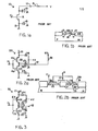
- the open drain output buffer comprises, in this example, N channel metal oxide silicon (MOS) transistor 16, having its source 13 grounded, its control gate 11 connected to a low power driving signal, and its drain 12 connected to output terminal 12 of the integrated circuit device.
- MOS metal oxide silicon
- a high voltage (logical 1) signal applied to gate 11 causes N channel transistor 16 to turn on, thus causing output terminal 12 to be grounded, which in turn causes current to flow through load device R L from voltage source V to terminal 12 to ground.
- a low voltage i.e. logical 0
- Parasitic diodes 19 and 15 i.e.
- transistor 16 comprises P type substrate 14, N type source 13, N type drain 12, field oxide region 98, gate insulation region 99, and control gate 11.
- Parasitic diode 15 is formed by the P N junction formed between P type substrate 14 and N type source 13.
- parasitic diode 19 is formed by the PN junction formed between P type substrate 14 and N type drain 12.
- Output buffer 20 is often referred to as the "CMOS Push-Pull" output stage, due to its use of complementary P channel and N channel transistors 22, 23, respectively.
- the source of P channel transistor 22 is connected to a positive voltage source V applied to terminal 21.
- the drain of P channel transistor 22 is connected to the drain of N channel transistors 23, and output terminal 12 is connected therebetween.
- the source of N channel transistor 23 is connected to ground.
- the gate lla of transistor 22 and the gate llb of transistor 2 3 are connected in common to terminal 11 which receive the input signal to be buffered by CMOS Push-Pull buffer stage 20.
- N type substrate 14 is connected to V and P type well region 81 is formed within substrate 14.
- P type well region 81 is connected to ground.
- P channel transistor 22 having its source connected to terminal 21, its drain connected to terminal 12,'and its control gate lla connected to terminal 11.
- the parasitic diodes 24 and 25 are formed by the PN junctions formed between the source and the drain of transistor 22 and N type substrate 14.
- N channel transistor 23 is formed in P type well 81 as shown.
- N channel transistor 23 has its source 39 grounded, its drain connected to terminal 12 and its gate llb connected to terminal 11.
- N channel transistor 23 has its parasitic diodes 26 and 27 formed by the PN junctions formed between P well 81 and the N type drain and source regions of transistor 23, respectively.
- the CMOS Push-Pull output buffer 20 is not suitable for use when it is desired to utilize an external pull-up resistor 95 in conjunction with an external pull-up voltage applied to terminal 93.
- the open drain output buffer circuit 10 of Figure la is, utilized because, as previously discussed, parasitic diode 19 ( Figure la) is reverse-biased and does not provide unwanted clamping of the external voltage applied to terminal 12.
- the reverse-bias breakdown voltage of parasitic diode 19 is typically on the order of 40 volts, and thus does not breakdown with typical pull up voltages.
- a single integrated circuit device such as a microprocessor is required by one user to have an output buffer configuration wherein certain output leads are provided as open drain output buffers, and other output leads are provided as CMOS Push-Pull output buffers, and is required by another user to have a different configuration of output buffers. Accordingly, prior to my present invention, it was heretofore required under such certain circumstances to produce a large number of separate products, each performing the same function but designed and fabricated to have different output buffer configurations.
- a structure wherein a single output buffer stage is provided which can be programmed to function either as an open drain output buffer or a CMOS Push-Pull output buffer.
- the output buffer stage constructed in accordance with this invention is programmed in one of several manners.
- the fabrication steps utilized to program the output buffer are the enhancement and depletion dopings, whereby certain devices of the output buffer are programmed to either remain always turned off or always turned on, thus programming the output buffer to serve either as an open drain output buffer or as a CMOS push-pull output buffer.
- FIG. 3 A schematic diagram of one form of a programmable output buffer stage is shown in Figure 3.
- the programmable output buffer stage 30 of Figure 3 is similar to the prior art CMOS Push-Pull output buffer stage 20 of Figure 2a.
- programmable conductive link 173 is used to connect the source of P channel transistor 22 with the drain of N channel transistor 23, when programmable output buffer stage 30 is to be used as a CMOS Push-Pull output stage.
- conductive link 173 is not formed, thus electrically isolating P channel transistor 22 and thus causing P channel transistor 22 to have no effect in the operation of output stage 30.
- output stage 30 functions as an open drain output buffer, with N channel transistor 23 performing the open drain output buffer function.
- Conductive link 173 may be formed in one of several manners.
- conductive link 173 may be formed as a fusible link which is destroyed by a programming current of sufficient magnitude to cause the fusible link to open.
- fusible link 173 will be left intact.
- fusible link 173 will be opened by the passage of a large amount of current therethrough.
- a major disadvantage to using fusible links to program the output buffer is that the fusible links can be damaged by the unintentional connection of an output lead of the device to a voltage greater than or equal to the programming voltage.
- the output buffer associated with that output lead will be programmed by the opening of its fusible link, thus providing an open drain output buffer where a CMOS Push-Pull output buffer is desired, thereby rendering the device useless. Accordingly, rather than the use of fusible links, other methods are preferred for programming output buffers.
- conductive link 173 is 'formed (or omitted) during the formation of an interconnect pattern on the surface of the integrated circuit die.
- This interconnect pattern is either a metalized layer (typically aluminum or an alloy of aluminum), polycrystalline silicon, or a diffused region.
- conductive link 173 will be formed, thus electrically connecting the drain of P channel transistor 22 to the drain of N channel transistor 23, when output buffer 30 is to operate as CMOS Push-Pull output buffer.
- conductive link 173 will be omitted, thus not providing electrical connection between the drain of P channel transistor 22 and the drain of N channel transistor 23, when output buffer 30 is to function as an open drain output buffer.
- the use of the metal mask to program output buffer'30 is desirable in that the metal interconnects are formed in a rather late stage of the processing of an integrated circuit device.
- many devices in which this programmable output stage may be used include other components which are programmed by the metal interconnect mask. For example, some read only memories (ROMS) are programmed by appropriate design of the metal interconnect pattern.
- ROMS read only memories
- the use of the metal interconnect pattern to program the output buffer is undesirable when other devices, such as ROM cells, are not programmed by use of the metal interconnect pattern, in that two unique programming masks are required to program each device type - one mask to program the ROM cells and either the metal mask or the contact mask to program the output buffers.
- Modern integrated circuit fabrication techniques discourage the use of the metal interconnect patterns as the means for programming ROM cells in that a significant reduction in ROM cell size (and thus a consequent increase in ROM packing density) is achieved by utilizing ROM cells which are programmed by the selective introduction of dopants so as to form selected ROM cells as either enhancement devices or, alternatively, as depletion devices.
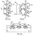
- the circuit of Figure 2a is formed with the addition of N channel transistor 43 connected in series between the source of P channel transistor 22 and the drain of N channel transistor 23.
- N channel transistor 43 acts as a switch.
- N channel transistor 43 With a logical 0 (low voltage) applied to the control gate 44 of N channel transistor 43, N channel transistor 43 turns off, thus electrically disconnecting the drain of transistor 22 from the drain of transistor 23, thus causing programmable output buffer 40 to operate as an open drain output buffer.
- N channel transistor 43 Conversely, with a logical 1 (high voltage) applied to the control gate 44 of N channel transistor 43, N channel transistor 43 conducts, thus connecting the drain of P channel transistor 22 to the drain of N channel transistor 23, thus causing programmable output buffer 40 ( Figure 4a) to function similarly to a CMOS Push-Pull output buffer.
- V the voltage available within the integrated circuit
- the output voltage corresponding to a logical 1 i.e. when P channel transistor 22 is on and N channel transistor 23 is off
- V T is the threshold voltage of N channel transistor 43.
- CMOS Push-Pull output buffers generally are required to provide a logical 1 output signal corresponding to V.
- a P channel MOS transistor cannot be used in place of N channel MOS transistor 43 because of the previously described problem of having a parasitic PN diode connected between output terminal 12 and ground which becomes forward biased when the output buffer 40 is used as an open drain output buffer (i.e. P channel switch 43 is off) with an external pull-up.
- the preferred embodiment of this invention is shown in the schematic diagram of Figure 5.
- Programmable output buffer 50 shown in Figure 5 is similar to the programmable output buffer 40 of Figure 4a.
- transistors 51 and 52 are provided and which in turn provide the appropriate bias voltage to control_gate 44 of N channel transistor 43 in order to program the output buffer 50 to operate either as a CMOS Push-Pull output buffer or, alternatively, as an open drain output buffer.
- transistor 51 comprises an N channel device having its drain connected to a positive voltage supply (V in this case) and its gate and source connected in common with both the drain of N channel transistor 52 and the control gate 44 of N channel transistor 43.
- the control gate and source of transistor 52 are connected in common with ground.
- the programmable output buffer is programmed to function as a CMOS Push-Pull output buffer in the following manner.
- P channel transistor 22, N channel transistor 23, and N channel transistor 52 are formed as enhancement devices.
- N channel enhancement devices require a minimum positive threshold voltage to exist between their gate and source in order for the N channel enhancement transistor to turn on.
- P channel enhancement transitors require a voltage equal to : or more negative than its negative threshold voltage to exist between its gate and source in order for the P channel enhancement transistor to turn on.
- N channel transistors 43 and 51 are formed as depletion devices.
- N channel depletion devices require a voltage greater than or equal to their negative threshold voltage to exist between their gate and source in order to turn on.
- N channel depletion transistor 51 With the gate and source of N channel depletion transistor 51 connected in common, their voltage difference is 0 which is above the negative threshold voltage of N channel depletion transistor 51. Thus, N channel depletion transistor 51 conducts. Similarly, with the control gate and source of N channel enhancement transistor 52 connected in common, their voltage difference is 0, which is less than the positive threshold voltage of N channel enhancement transistor 52, thus causing transistor 52 to remain off. In this manner, the positive voltage V is applied through conducting depletion transistor 51 to the control gate 44 of N channel depletion transistor 43.
- transistor 43 provides a low impedance path connecting the drain of P channel transistor 22 with the drain of N channel transistor 23, thus causing programmable output stage 50 to operate as a CMOS Push-Pull output buffer.
- programmable output buffer 50 is programmed to function as an open drain output buffer in the following manner.
- P channel transistor 22, N channel transistor 23, N channel transistor 43, and N channel transistor 51 are fabricated as enhancement : devices.
- N channel transistor 52 is formed as a depletion device. With N channel transistor 51 formed an enhancement device, and the voltage between its gate and source, which are connected in common, equal to zero, enhancement device 51 will remain off. Conversely, because N channel transistor 52 is formed as a depletion device and the voltage between its gate and source, which are connected in common, is zero, which is above its negative threshold voltage, depletion device 52 will remain on. With depletion device 52 on, the control gate 44 of N channel enhancement transistor 43 is effectively grounded.
- control gate 44 and the source of transistor 43 will never be greater than the positive threshold voltage of enhancement transistor 43 and thus transistor 43 will remain off. with transistor 43 turned off, P channel transistor 22 is effectively disconnected, thus causing N channel transistor 23 to provide an open drain output buffer.
- the external pull up voltage applied to output terminal 12 cannot exceed the source to drain breakdown voltage of N channel transistor 43, or transistor 43 will not function as an open switch, and output buffer 50 will not function properly.
- the source to drain breakdown voltage of N channel enhancement transistor 43 is on the order of 15 volts, which is well above the typical external pull up voltage that is applied to terminal 12 when output buffer 50 is used as an open drain output buffer.
- CMOS complementary metal oxide silicon
- the CMOS ° devices having-gate oxide thickness of approximately 650A are formed in an N type silicon substrate having crystal : orientation (100) and resistivity of approximately 2-4 ohm-centimeter.
- a P type well region is formed within the N type substrate by the implantation of boron ions at approximately 100 KEV to a dosage of approximately 7x10 12 atoms/cm 2 and driven by an oxidation in dry oxygen at approximately 1150°C for approximately 500 minutes.
- Arsenic ions are selectively implanted at approximately 100 KEV to a dosage of approximately 3x10 12 atoms/cm 2 into the to-be-formed N type channel regions of the to-be-formed N channel depletion transistors, thus providing an N channel depletion device threshold voltage of approximately - 5 volts.
- P channel threshold voltage adjustment is performed by the ion implantation of boron ions at approximately 4 0 KEV to a dosage of approximately 2x10 11 atoms/cm 2 , thus providing a P channel threshold voltage of approximately -0.8 volts.
- N+ source/drain regions are then formed in the P well by the implantation of arsenic ions at approximately 40 KEV to a dosage of approximately 5x10 15 atoms/cm 2 .
- the N+ source/drain regions are then driven by the formation of a layer of oxide covering the N+ source/drain regions which is formed by thermal oxidation in dry oxygen at a temperature of approximately 1000°C for approximately 40 minutes.
- P+ source/drain regions are then formed in the N type substrate by the ion implantation of boron ions at approimxately 30 KEV to a dosage of approximately 5x1 0 15 atoms/cm 2 .
- This technique provides N channel and P channel enhancement transistors having threshold voltages of approximately +0.8 volts and -0.8 volts, respectively, as well as N channel depletion transistors which have a threshold voltage of approximately -5.0 volts.
Landscapes
- Physics & Mathematics (AREA)
- Nonlinear Science (AREA)
- Metal-Oxide And Bipolar Metal-Oxide Semiconductor Integrated Circuits (AREA)
- Logic Circuits (AREA)
Applications Claiming Priority (2)
| Application Number | Priority Date | Filing Date | Title |
|---|---|---|---|
| US386125 | 1982-06-07 | ||
| US06/386,125 US4481432A (en) | 1982-06-07 | 1982-06-07 | Programmable output buffer |
Publications (1)
| Publication Number | Publication Date |
|---|---|
| EP0096637A1 true EP0096637A1 (de) | 1983-12-21 |
Family
ID=23524271
Family Applications (1)
| Application Number | Title | Priority Date | Filing Date |
|---|---|---|---|
| EP83401125A Withdrawn EP0096637A1 (de) | 1982-06-07 | 1983-06-03 | Programmierbarer Ausgangspuffer |
Country Status (3)
| Country | Link |
|---|---|
| US (1) | US4481432A (de) |
| EP (1) | EP0096637A1 (de) |
| CA (1) | CA1196427A (de) |
Cited By (4)
| Publication number | Priority date | Publication date | Assignee | Title |
|---|---|---|---|---|
| GB2178618A (en) * | 1985-07-27 | 1987-02-11 | Stc Plc | Input buffer circuit for static ram |
| EP0351896A3 (de) * | 1988-06-22 | 1991-02-27 | Lsi Logic Corporation | Logische bi-CMOS Matrix |
| EP0498377A3 (en) * | 1991-02-07 | 1993-12-22 | Rohm Co Ltd | Output circuit |
| EP0651510A1 (de) * | 1993-10-29 | 1995-05-03 | STMicroelectronics S.r.l. | Zum Arbeiten mit niedrigen und hohen Spannungen geeignete Eingangs-/Ausgangsstufe |
Families Citing this family (19)
| Publication number | Priority date | Publication date | Assignee | Title |
|---|---|---|---|---|
| JPS58137327A (ja) * | 1982-02-10 | 1983-08-15 | Toshiba Corp | 半導体集積回路 |
| US4556806A (en) * | 1982-05-10 | 1985-12-03 | Texas Instruments Incorporated | Gate alterable output buffer |
| US4652773A (en) * | 1982-09-30 | 1987-03-24 | Rca Corporation | Integrated circuits with electrically erasable electrically programmable latch circuits therein for controlling operation |
| US4704547A (en) * | 1984-12-10 | 1987-11-03 | American Telephone And Telegraph Company, At&T Bell Laboratories | IGFET gating circuit having reduced electric field degradation |
| US4709162A (en) * | 1986-09-18 | 1987-11-24 | International Business Machines Corporation | Off-chip driver circuits |
| US4833349A (en) * | 1987-09-01 | 1989-05-23 | Plx Technology | Programmable logic and driver circuits |
| US5036224A (en) * | 1990-03-01 | 1991-07-30 | National Semiconductor Corporation | Single ended MOS to ECL output buffer |
| JP3556679B2 (ja) | 1992-05-29 | 2004-08-18 | 株式会社半導体エネルギー研究所 | 電気光学装置 |
| US5237221A (en) * | 1991-11-25 | 1993-08-17 | Hewlett-Packard Company | On-chip pull-up circuit which may be selectively disabled |
| US5488317A (en) * | 1993-10-22 | 1996-01-30 | Texas Instruments Incorporated | Wired logic functions on FPGA's |
| DE19527736C1 (de) * | 1995-07-28 | 1996-11-14 | Texas Instruments Deutschland | Schaltungsanordnung zur Ansteuerung eines dem Speisekreis einer elektrischen Last zugeordneten MOS-Feldeffekttransistors |
| US5656951A (en) * | 1996-02-05 | 1997-08-12 | Motorola, Inc. | Input circuit and method for holding data in mixed power supply mode |
| JP3190843B2 (ja) * | 1996-12-09 | 2001-07-23 | 日本電気株式会社 | プログラム可能なバッファ回路 |
| US6624661B2 (en) * | 2001-08-16 | 2003-09-23 | Via Technologies, Inc. | Programmable drive circuit for I/O port |
| US6580290B1 (en) | 2002-01-22 | 2003-06-17 | Agilent Technologies, Inc. | Open collector/drain and SSTL compliant output driver circuit and method for operating the circuit |
| KR100482367B1 (ko) * | 2002-08-09 | 2005-04-13 | 삼성전자주식회사 | 반도체 메모리장치의 데이터 출력버퍼 및 그 데이터출력방법 |
| CN103928464B (zh) * | 2014-04-18 | 2015-08-12 | 杭州士兰微电子股份有限公司 | 复合器件及开关电源 |
| TWI715224B (zh) * | 2019-09-30 | 2021-01-01 | 瑞昱半導體股份有限公司 | 具有耐壓機制的輸出電路 |
| US11881859B2 (en) * | 2022-05-20 | 2024-01-23 | Texas Instruments Incorporated | Schmitt trigger circuit having mismatched input and supply |
Citations (3)
| Publication number | Priority date | Publication date | Assignee | Title |
|---|---|---|---|---|
| US4223277A (en) * | 1978-12-27 | 1980-09-16 | Harris Corporation | Electrically alterable field effect transistor amplifier configuration |
| EP0020778A1 (de) * | 1978-11-17 | 1981-01-07 | Fujitsu Limited | Verstärkerschaltung |
| US4295209A (en) * | 1979-11-28 | 1981-10-13 | General Motors Corporation | Programming an IGFET read-only-memory |
Family Cites Families (7)
| Publication number | Priority date | Publication date | Assignee | Title |
|---|---|---|---|---|
| US3651340A (en) * | 1970-06-22 | 1972-03-21 | Hamilton Watch Co | Current limiting complementary symmetry mos inverters |
| JPS588588B2 (ja) * | 1975-05-28 | 1983-02-16 | 株式会社日立製作所 | 半導体集積回路 |
| JPS525254A (en) * | 1975-07-02 | 1977-01-14 | Hitachi Ltd | High voltage resistance mis switching circuit |
| US4209713A (en) * | 1975-07-18 | 1980-06-24 | Tokyo Shibaura Electric Co., Ltd. | Semiconductor integrated circuit device in which difficulties caused by parasitic transistors are eliminated |
| JPS5939904B2 (ja) * | 1978-09-28 | 1984-09-27 | 株式会社東芝 | 半導体装置 |
| US4274014A (en) * | 1978-12-01 | 1981-06-16 | Rca Corporation | Switched current source for current limiting complementary symmetry inverter |
| JPS56111180A (en) * | 1980-02-06 | 1981-09-02 | Toshiba Corp | Semiconductor device |
-
1982
- 1982-06-07 US US06/386,125 patent/US4481432A/en not_active Expired - Lifetime
-
1983
- 1983-06-03 EP EP83401125A patent/EP0096637A1/de not_active Withdrawn
- 1983-06-06 CA CA000429765A patent/CA1196427A/en not_active Expired
Patent Citations (3)
| Publication number | Priority date | Publication date | Assignee | Title |
|---|---|---|---|---|
| EP0020778A1 (de) * | 1978-11-17 | 1981-01-07 | Fujitsu Limited | Verstärkerschaltung |
| US4223277A (en) * | 1978-12-27 | 1980-09-16 | Harris Corporation | Electrically alterable field effect transistor amplifier configuration |
| US4295209A (en) * | 1979-11-28 | 1981-10-13 | General Motors Corporation | Programming an IGFET read-only-memory |
Cited By (4)
| Publication number | Priority date | Publication date | Assignee | Title |
|---|---|---|---|---|
| GB2178618A (en) * | 1985-07-27 | 1987-02-11 | Stc Plc | Input buffer circuit for static ram |
| EP0351896A3 (de) * | 1988-06-22 | 1991-02-27 | Lsi Logic Corporation | Logische bi-CMOS Matrix |
| EP0498377A3 (en) * | 1991-02-07 | 1993-12-22 | Rohm Co Ltd | Output circuit |
| EP0651510A1 (de) * | 1993-10-29 | 1995-05-03 | STMicroelectronics S.r.l. | Zum Arbeiten mit niedrigen und hohen Spannungen geeignete Eingangs-/Ausgangsstufe |
Also Published As
| Publication number | Publication date |
|---|---|
| CA1196427A (en) | 1985-11-05 |
| US4481432A (en) | 1984-11-06 |
Similar Documents
| Publication | Publication Date | Title |
|---|---|---|
| US4481432A (en) | Programmable output buffer | |
| US5837554A (en) | Integrated circuit with EPROM cells | |
| US4387503A (en) | Method for programming circuit elements in integrated circuits | |
| JP3992855B2 (ja) | 静電気放電保護のための回路 | |
| US4312046A (en) | Vertical fuse and method of fabrication | |
| EP0305676A2 (de) | CMOS-Ausgangstreiberschaltung | |
| JPH04290008A (ja) | オフ・チップ・ドライバ回路 | |
| US20010011734A1 (en) | Semiconductor device having a library of standard cells and method of designing the same | |
| US5838033A (en) | Integrated circuit with gate conductor defined resistor | |
| US4609931A (en) | Input protection MOS semiconductor device with zener breakdown mechanism | |
| JPH07130963A (ja) | モノリシック集積回路と保護装置 | |
| JPH0210678Y2 (de) | ||
| EP0700090A1 (de) | Integrierte Halbleiterschaltung mit einer Stromspiegelschaltung | |
| US5789781A (en) | Silicon-on-insulator (SOI) semiconductor device and method of making the same | |
| HK79493A (en) | Integrated circuit of the complementary technique having a substrate bias generator | |
| US5525829A (en) | Field effect transistor with integrated schottky diode clamp | |
| US4892836A (en) | Method for manufacturing semiconductor integrated circuits including CMOS and high-voltage electronic devices | |
| US5489797A (en) | Local interconnect structure | |
| US6369606B1 (en) | Mixed threshold voltage CMOS logic device and method of manufacture therefor | |
| KR100228035B1 (ko) | 저전압출력회로 및 반도체장치 | |
| EP0242523A2 (de) | Integrierte Steuerungsstufe für logische FET-Schaltung | |
| EP0092176A2 (de) | Basiszelle für integrierte Verknüpfungsschaltungsfelder | |
| KR0163459B1 (ko) | 3개의 전원 공급선을 갖는 출력 회로 | |
| US4952824A (en) | Ion implantation programmable logic device | |
| US5856218A (en) | Bipolar transistor formed by a high energy ion implantation method |
Legal Events
| Date | Code | Title | Description |
|---|---|---|---|
| PUAI | Public reference made under article 153(3) epc to a published international application that has entered the european phase |
Free format text: ORIGINAL CODE: 0009012 |
|
| AK | Designated contracting states |
Designated state(s): DE FR GB IT NL |
|
| 17P | Request for examination filed |
Effective date: 19840612 |
|
| 17Q | First examination report despatched |
Effective date: 19860321 |
|
| STAA | Information on the status of an ep patent application or granted ep patent |
Free format text: STATUS: THE APPLICATION IS DEEMED TO BE WITHDRAWN |
|
| 18D | Application deemed to be withdrawn |
Effective date: 19870220 |
|
| RIN1 | Information on inventor provided before grant (corrected) |
Inventor name: DAVIES, THOMAS J. |