EP0096872B1 - Etage d'émission pour signaux numériques à grande vitesse - Google Patents
Etage d'émission pour signaux numériques à grande vitesse Download PDFInfo
- Publication number
- EP0096872B1 EP0096872B1 EP83105719A EP83105719A EP0096872B1 EP 0096872 B1 EP0096872 B1 EP 0096872B1 EP 83105719 A EP83105719 A EP 83105719A EP 83105719 A EP83105719 A EP 83105719A EP 0096872 B1 EP0096872 B1 EP 0096872B1
- Authority
- EP
- European Patent Office
- Prior art keywords
- transistor
- terminal
- resistor
- reference potential
- collector
- Prior art date
- Legal status (The legal status is an assumption and is not a legal conclusion. Google has not performed a legal analysis and makes no representation as to the accuracy of the status listed.)
- Expired
Links
Images
Classifications
-
- H—ELECTRICITY
- H04—ELECTRIC COMMUNICATION TECHNIQUE
- H04L—TRANSMISSION OF DIGITAL INFORMATION, e.g. TELEGRAPHIC COMMUNICATION
- H04L25/00—Baseband systems
- H04L25/38—Synchronous or start-stop systems, e.g. for Baudot code
- H04L25/40—Transmitting circuits; Receiving circuits
- H04L25/49—Transmitting circuits; Receiving circuits using code conversion at the transmitter; using predistortion; using insertion of idle bits for obtaining a desired frequency spectrum; using three or more amplitude levels ; Baseband coding techniques specific to data transmission systems
- H04L25/4917—Transmitting circuits; Receiving circuits using code conversion at the transmitter; using predistortion; using insertion of idle bits for obtaining a desired frequency spectrum; using three or more amplitude levels ; Baseband coding techniques specific to data transmission systems using multilevel codes
- H04L25/4923—Transmitting circuits; Receiving circuits using code conversion at the transmitter; using predistortion; using insertion of idle bits for obtaining a desired frequency spectrum; using three or more amplitude levels ; Baseband coding techniques specific to data transmission systems using multilevel codes using ternary codes
- H04L25/4925—Transmitting circuits; Receiving circuits using code conversion at the transmitter; using predistortion; using insertion of idle bits for obtaining a desired frequency spectrum; using three or more amplitude levels ; Baseband coding techniques specific to data transmission systems using multilevel codes using ternary codes using balanced bipolar ternary codes
Definitions
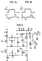
- the second npn transistor T2 includes an input E for the digital signal to be amplified, which is connected to the base connection of a first npn transistor T1, and an input E for the inverse digital signal, which is connected to the base connection of a second npn transistor T2 is connected.
- the emitter connections of both transistors are connected to one another and, via a first resistor R1, to a source for a negative operating voltage -Ub. This results in a push-pull driven emitter-coupled differential amplifier on the input side.
- the collector terminal of the first transistor T1 is connected to the reference potential via a series circuit of a second resistor R2 and a first inductor L1.
- the first inductor L1 acts as a compensation inductor, which is damped by the comparatively low-impedance resistor R2 and provides for an increase in the height of the signal amplified by the first emitter-coupled differential amplifier.
- the collector of the first transistor T1 is connected to the base terminal of a third transistor T3 via a DC coupling element formed from a first Zener diode D1 and a first resistor C1 connected in parallel therewith.
- the base connection of the third transistor T3 is also connected via a third resistor R3 to the operating voltage source -Ub, to which the base connection of the fourth transistor T4 is also connected via a fifth resistor R5.
- the emitter connections of the third and fourth transistor T3, T4 are connected to one another and to the operating voltage source -Ub via a sixth resistor R6, so that the output stage transistors also form an emitter-coupled differential amplifier.
- the collector connection of the fourth transistor T4 is connected directly to reference potential, while the collector connection of the third transistor T3 is connected to the operating voltage source -Ub via a protective diode D6 which is polarized in the reverse direction during normal operation, and via a series circuit comprising three protective diodes D3, D4 which are polarized in the reverse direction during normal operation , D5 and connected in parallel via a second inductor L2 in the form of a high-frequency choke with reference potential.
- the diode series connection like the high-frequency choke, is used to discharge overvoltages that come from the connected cable section KK to the transmitter stage.
- an RC element is also used, which is connected on one side to the collector terminal of the third transistor T3, consists of the parallel connection of a relatively low-resistance seventh resistor R7 and a third capacitor C3 and is also connected to the inner conductor of the connected coaxial cable .
- a third inductor L3 in the form of a remote feed choke is also connected to the inner conductor of the coaxial cable KK.
- the remote feed choke is replaced in a manner known per se by a spur line KL, which at the end is short-circuited and connected Reference potential is connected, while on the other side one connection is connected to the reference potential and the other to the inner conductor of the coaxial cable.
- the length of the stub line is chosen so that the simple transit time of the pulses in the stub line corresponds to half a bit duration of the binary input pulses. The reflection of a voltage jump at the short-circuited end of the stub line thus leads, at intervals of one bit, to a second pulse which has the opposite polarity to the first pulse or the first pulse edge.
- a seventh diode D7 reverse-biased protective diode is connected between emitter and base of third transistor T3 and an eighth diode D8 reverse-biased protective diode between emitter and base of fourth transistor T4.
Landscapes
- Physics & Mathematics (AREA)
- Spectroscopy & Molecular Physics (AREA)
- Engineering & Computer Science (AREA)
- Computer Networks & Wireless Communication (AREA)
- Signal Processing (AREA)
- Dc Digital Transmission (AREA)
- Reduction Or Emphasis Of Bandwidth Of Signals (AREA)
- Investigating Or Analysing Biological Materials (AREA)
- Television Systems (AREA)
- Electrophonic Musical Instruments (AREA)
- Amplifiers (AREA)
- Static Random-Access Memory (AREA)
Claims (4)
Priority Applications (1)
| Application Number | Priority Date | Filing Date | Title |
|---|---|---|---|
| AT83105719T ATE37642T1 (de) | 1982-06-14 | 1983-06-10 | Sendestufe fuer digitale signale hoher schrittgeschwindigkeit. |
Applications Claiming Priority (2)
| Application Number | Priority Date | Filing Date | Title |
|---|---|---|---|
| DE19823222341 DE3222341A1 (de) | 1982-06-14 | 1982-06-14 | Sendestufe fuer digitale signale hoher schrittgeschwindigkeit |
| DE3222341 | 1982-06-14 |
Publications (3)
| Publication Number | Publication Date |
|---|---|
| EP0096872A2 EP0096872A2 (fr) | 1983-12-28 |
| EP0096872A3 EP0096872A3 (en) | 1986-08-20 |
| EP0096872B1 true EP0096872B1 (fr) | 1988-09-28 |
Family
ID=6166041
Family Applications (1)
| Application Number | Title | Priority Date | Filing Date |
|---|---|---|---|
| EP83105719A Expired EP0096872B1 (fr) | 1982-06-14 | 1983-06-10 | Etage d'émission pour signaux numériques à grande vitesse |
Country Status (6)
| Country | Link |
|---|---|
| EP (1) | EP0096872B1 (fr) |
| JP (1) | JPS58223942A (fr) |
| AT (1) | ATE37642T1 (fr) |
| DE (2) | DE3222341A1 (fr) |
| FI (1) | FI832119A7 (fr) |
| NO (1) | NO831883L (fr) |
Family Cites Families (7)
| Publication number | Priority date | Publication date | Assignee | Title |
|---|---|---|---|---|
| NL245607A (fr) * | 1959-01-19 | |||
| DE1295660B (de) * | 1965-04-07 | 1969-05-22 | North American Aviation Inc | Zweistufiger direktgekoppelter Gleichstromdifferenzverstaerker |
| US3639785A (en) * | 1969-01-21 | 1972-02-01 | Tektronix Inc | Pulse generator |
| US3978349A (en) * | 1974-09-03 | 1976-08-31 | Rca Corporation | Switching circuit |
| DE2503384C3 (de) * | 1975-01-28 | 1982-10-14 | Siemens AG, 1000 Berlin und 8000 München | Differenzverstärker für den Subnanosekundenbereich |
| DE2804086B2 (de) * | 1978-01-31 | 1979-12-06 | Siemens Ag, 1000 Berlin Und 8000 Muenchen | Verfahren zum Ein- und Auskoppeln eines breitbandigen Impuls-Signals an eine Kabelstrecke mit ferngespeisten Zwischenverstärkerstellen |
| FR2420886A1 (fr) * | 1978-03-24 | 1979-10-19 | Telecommunications Sa | Amplificateur de sortie pour systeme de regeneration de signaux numeriques transmis en code ternaire |
-
1982
- 1982-06-14 DE DE19823222341 patent/DE3222341A1/de not_active Withdrawn
-
1983
- 1983-05-27 NO NO831883A patent/NO831883L/no unknown
- 1983-05-31 JP JP58095116A patent/JPS58223942A/ja active Pending
- 1983-06-10 DE DE8383105719T patent/DE3378153D1/de not_active Expired
- 1983-06-10 EP EP83105719A patent/EP0096872B1/fr not_active Expired
- 1983-06-10 AT AT83105719T patent/ATE37642T1/de not_active IP Right Cessation
- 1983-06-13 FI FI832119A patent/FI832119A7/fi not_active Application Discontinuation
Also Published As
| Publication number | Publication date |
|---|---|
| EP0096872A2 (fr) | 1983-12-28 |
| FI832119L (fi) | 1983-12-15 |
| EP0096872A3 (en) | 1986-08-20 |
| NO831883L (no) | 1983-12-15 |
| DE3222341A1 (de) | 1983-12-15 |
| FI832119A7 (fi) | 1983-12-15 |
| FI832119A0 (fi) | 1983-06-13 |
| JPS58223942A (ja) | 1983-12-26 |
| ATE37642T1 (de) | 1988-10-15 |
| DE3378153D1 (en) | 1988-11-03 |
Similar Documents
| Publication | Publication Date | Title |
|---|---|---|
| DE2813628A1 (de) | Filterschaltung | |
| EP0371558B1 (fr) | Circuit pour équipements de transmission | |
| DE2903860A1 (de) | Einrichtung zur gleichstromversorgung eines verbrauchers und zur gleichzeitigen informationsuebertragung ueber ein aderpaar | |
| DE3633518A1 (de) | Getakteter gleichspannungswandler | |
| EP0096872A2 (fr) | Etage d'émission pour signaux numériques à grande vitesse | |
| DE3901589A1 (de) | Ankopplung eines busteilnehmers | |
| DE3117927C2 (de) | Anordnung zur Erkennung der längsten von in digitalen Signalen periodisch enthaltenen Folgen von Nullzeichen | |
| DE2462048C2 (de) | Schaltungsanordnung für einen Telefonapparat mit Wahltastatur | |
| DE4140904A1 (de) | Uebertragungsvorrichtung | |
| DE2843213C2 (de) | Schaltungsanordnung zur Spannungsbegrenzung | |
| DE2063517A1 (de) | Schaltungsanordnung zur Erzeugung von Impulsen, die den Kennzeitpunkten der Modulation eines Telegraphiezeichens ent sprechen | |
| DE2411377C3 (de) | Schaltungsanordnung für einen Telefonapparat mit Wähltastatur | |
| EP0004008B1 (fr) | Discriminateur d'amplitude rapide pour signaux numériques | |
| EP0130139A1 (fr) | Montage pour la saisie électriquement isolée de signaux électriques binaires | |
| DE3303904C1 (de) | Schaltung zum Übertragen eines Schaltsignals | |
| EP0164014A1 (fr) | Moyen d'excitation de relais | |
| DE1083350B (de) | Schaltungsanordnung zur Auswertung von Mehrfrequenzenkodezeichen | |
| DE2417644C3 (de) | PCM-Regenerator | |
| DE2202749A1 (de) | Sperrschaltung fuer Stoersignale | |
| DE2603548C2 (de) | Pegelumsetzer für vermittlungstechnische Zeichen | |
| DE2504823B2 (de) | Elektronischer schalter | |
| DE4228010C2 (de) | Leitungsempfänger | |
| DE19916686A1 (de) | Eingangsschaltung für relativ hochstromige zu überwachende AC-Signale | |
| EP0499869A1 (fr) | Circuit pour génération de tension alternative | |
| DE9209246U1 (de) | Anordnung zum Ankoppeln eines Teilnehmers an die Busleitung eines Bussystems, insbesondere für den Einsatz im Bergbau unter Tage |
Legal Events
| Date | Code | Title | Description |
|---|---|---|---|
| PUAI | Public reference made under article 153(3) epc to a published international application that has entered the european phase |
Free format text: ORIGINAL CODE: 0009012 |
|
| AK | Designated contracting states |
Designated state(s): AT BE CH DE FR GB IT LI LU NL SE |
|
| 17P | Request for examination filed |
Effective date: 19841219 |
|
| PUAL | Search report despatched |
Free format text: ORIGINAL CODE: 0009013 |
|
| AK | Designated contracting states |
Kind code of ref document: A3 Designated state(s): AT BE CH DE FR GB IT LI LU NL SE |
|
| 17Q | First examination report despatched |
Effective date: 19871104 |
|
| GRAA | (expected) grant |
Free format text: ORIGINAL CODE: 0009210 |
|
| AK | Designated contracting states |
Kind code of ref document: B1 Designated state(s): AT BE CH DE FR GB IT LI LU NL SE |
|
| PG25 | Lapsed in a contracting state [announced via postgrant information from national office to epo] |
Ref country code: SE Effective date: 19880928 Ref country code: NL Effective date: 19880928 Ref country code: IT Free format text: LAPSE BECAUSE OF FAILURE TO SUBMIT A TRANSLATION OF THE DESCRIPTION OR TO PAY THE FEE WITHIN THE PRESCRIBED TIME-LIMIT;WARNING: LAPSES OF ITALIAN PATENTS WITH EFFECTIVE DATE BEFORE 2007 MAY HAVE OCCURRED AT ANY TIME BEFORE 2007. THE CORRECT EFFECTIVE DATE MAY BE DIFFERENT FROM THE ONE RECORDED. Effective date: 19880928 Ref country code: GB Free format text: LAPSE BECAUSE OF NON-PAYMENT OF DUE FEES Effective date: 19880928 Ref country code: FR Free format text: THE PATENT HAS BEEN ANNULLED BY A DECISION OF A NATIONAL AUTHORITY Effective date: 19880928 Ref country code: BE Effective date: 19880928 |
|
| REF | Corresponds to: |
Ref document number: 37642 Country of ref document: AT Date of ref document: 19881015 Kind code of ref document: T |
|
| REF | Corresponds to: |
Ref document number: 3378153 Country of ref document: DE Date of ref document: 19881103 |
|
| EN | Fr: translation not filed | ||
| NLV1 | Nl: lapsed or annulled due to failure to fulfill the requirements of art. 29p and 29m of the patents act | ||
| GBV | Gb: ep patent (uk) treated as always having been void in accordance with gb section 77(7)/1977 [no translation filed] | ||
| PG25 | Lapsed in a contracting state [announced via postgrant information from national office to epo] |
Ref country code: LU Free format text: LAPSE BECAUSE OF NON-PAYMENT OF DUE FEES Effective date: 19890630 Ref country code: LI Effective date: 19890630 Ref country code: CH Effective date: 19890630 |
|
| PLBE | No opposition filed within time limit |
Free format text: ORIGINAL CODE: 0009261 |
|
| STAA | Information on the status of an ep patent application or granted ep patent |
Free format text: STATUS: NO OPPOSITION FILED WITHIN TIME LIMIT |
|
| 26N | No opposition filed | ||
| REG | Reference to a national code |
Ref country code: CH Ref legal event code: PL |
|
| PGFP | Annual fee paid to national office [announced via postgrant information from national office to epo] |
Ref country code: AT Payment date: 19910529 Year of fee payment: 9 |
|
| PGFP | Annual fee paid to national office [announced via postgrant information from national office to epo] |
Ref country code: DE Payment date: 19910827 Year of fee payment: 9 |
|
| PG25 | Lapsed in a contracting state [announced via postgrant information from national office to epo] |
Ref country code: AT Effective date: 19920610 |
|
| PG25 | Lapsed in a contracting state [announced via postgrant information from national office to epo] |
Ref country code: DE Effective date: 19930302 |