EP0097058A2 - Gesinterter Gegenstand aus Siliciumcarbid mit metallisierter Schicht und Verfahren zu seiner Herstellung - Google Patents
Gesinterter Gegenstand aus Siliciumcarbid mit metallisierter Schicht und Verfahren zu seiner Herstellung Download PDFInfo
- Publication number
- EP0097058A2 EP0097058A2 EP83303456A EP83303456A EP0097058A2 EP 0097058 A2 EP0097058 A2 EP 0097058A2 EP 83303456 A EP83303456 A EP 83303456A EP 83303456 A EP83303456 A EP 83303456A EP 0097058 A2 EP0097058 A2 EP 0097058A2
- Authority
- EP
- European Patent Office
- Prior art keywords
- sintered body
- metallized layer
- sic
- binder
- layer
- Prior art date
- Legal status (The legal status is an assumption and is not a legal conclusion. Google has not performed a legal analysis and makes no representation as to the accuracy of the status listed.)
- Granted
Links
Images


Classifications
-
- C—CHEMISTRY; METALLURGY
- C04—CEMENTS; CONCRETE; ARTIFICIAL STONE; CERAMICS; REFRACTORIES
- C04B—LIME, MAGNESIA; SLAG; CEMENTS; COMPOSITIONS THEREOF, e.g. MORTARS, CONCRETE OR LIKE BUILDING MATERIALS; ARTIFICIAL STONE; CERAMICS; REFRACTORIES; TREATMENT OF NATURAL STONE
- C04B41/00—After-treatment of mortars, concrete, artificial stone or ceramics; Treatment of natural stone
- C04B41/45—Coating or impregnating, e.g. injection in masonry, partial coating of green or fired ceramics, organic coating compositions for adhering together two concrete elements
- C04B41/52—Multiple coating or impregnating multiple coating or impregnating with the same composition or with compositions only differing in the concentration of the constituents, is classified as single coating or impregnation
-
- C—CHEMISTRY; METALLURGY
- C04—CEMENTS; CONCRETE; ARTIFICIAL STONE; CERAMICS; REFRACTORIES
- C04B—LIME, MAGNESIA; SLAG; CEMENTS; COMPOSITIONS THEREOF, e.g. MORTARS, CONCRETE OR LIKE BUILDING MATERIALS; ARTIFICIAL STONE; CERAMICS; REFRACTORIES; TREATMENT OF NATURAL STONE
- C04B37/00—Joining burned ceramic articles with other burned ceramic articles or other articles by heating
- C04B37/02—Joining burned ceramic articles with other burned ceramic articles or other articles by heating with metallic articles
- C04B37/023—Joining burned ceramic articles with other burned ceramic articles or other articles by heating with metallic articles characterised by the interlayer used
- C04B37/025—Joining burned ceramic articles with other burned ceramic articles or other articles by heating with metallic articles characterised by the interlayer used consisting of glass or ceramic material
-
- C—CHEMISTRY; METALLURGY
- C04—CEMENTS; CONCRETE; ARTIFICIAL STONE; CERAMICS; REFRACTORIES
- C04B—LIME, MAGNESIA; SLAG; CEMENTS; COMPOSITIONS THEREOF, e.g. MORTARS, CONCRETE OR LIKE BUILDING MATERIALS; ARTIFICIAL STONE; CERAMICS; REFRACTORIES; TREATMENT OF NATURAL STONE
- C04B41/00—After-treatment of mortars, concrete, artificial stone or ceramics; Treatment of natural stone
- C04B41/80—After-treatment of mortars, concrete, artificial stone or ceramics; Treatment of natural stone of only ceramics
- C04B41/81—Coating or impregnation
- C04B41/89—Coating or impregnation for obtaining at least two superposed coatings having different compositions
-
- H—ELECTRICITY
- H10—SEMICONDUCTOR DEVICES; ELECTRIC SOLID-STATE DEVICES NOT OTHERWISE PROVIDED FOR
- H10W—GENERIC PACKAGES, INTERCONNECTIONS, CONNECTORS OR OTHER CONSTRUCTIONAL DETAILS OF DEVICES COVERED BY CLASS H10
- H10W40/00—Arrangements for thermal protection or thermal control
- H10W40/20—Arrangements for cooling
- H10W40/25—Arrangements for cooling characterised by their materials
- H10W40/259—Ceramics or glasses
-
- H—ELECTRICITY
- H10—SEMICONDUCTOR DEVICES; ELECTRIC SOLID-STATE DEVICES NOT OTHERWISE PROVIDED FOR
- H10W—GENERIC PACKAGES, INTERCONNECTIONS, CONNECTORS OR OTHER CONSTRUCTIONAL DETAILS OF DEVICES COVERED BY CLASS H10
- H10W70/00—Package substrates; Interposers; Redistribution layers [RDL]
- H10W70/01—Manufacture or treatment
- H10W70/05—Manufacture or treatment of insulating or insulated package substrates, or of interposers, or of redistribution layers
- H10W70/098—Applying pastes or inks, e.g. screen printing
-
- H—ELECTRICITY
- H10—SEMICONDUCTOR DEVICES; ELECTRIC SOLID-STATE DEVICES NOT OTHERWISE PROVIDED FOR
- H10W—GENERIC PACKAGES, INTERCONNECTIONS, CONNECTORS OR OTHER CONSTRUCTIONAL DETAILS OF DEVICES COVERED BY CLASS H10
- H10W70/00—Package substrates; Interposers; Redistribution layers [RDL]
- H10W70/60—Insulating or insulated package substrates; Interposers; Redistribution layers
- H10W70/67—Insulating or insulated package substrates; Interposers; Redistribution layers characterised by their insulating layers or insulating parts
- H10W70/69—Insulating materials thereof
- H10W70/692—Ceramics or glasses
-
- C—CHEMISTRY; METALLURGY
- C04—CEMENTS; CONCRETE; ARTIFICIAL STONE; CERAMICS; REFRACTORIES
- C04B—LIME, MAGNESIA; SLAG; CEMENTS; COMPOSITIONS THEREOF, e.g. MORTARS, CONCRETE OR LIKE BUILDING MATERIALS; ARTIFICIAL STONE; CERAMICS; REFRACTORIES; TREATMENT OF NATURAL STONE
- C04B2237/00—Aspects relating to ceramic laminates or to joining of ceramic articles with other articles by heating
- C04B2237/02—Aspects relating to interlayers, e.g. used to join ceramic articles with other articles by heating
- C04B2237/04—Ceramic interlayers
- C04B2237/06—Oxidic interlayers
-
- C—CHEMISTRY; METALLURGY
- C04—CEMENTS; CONCRETE; ARTIFICIAL STONE; CERAMICS; REFRACTORIES
- C04B—LIME, MAGNESIA; SLAG; CEMENTS; COMPOSITIONS THEREOF, e.g. MORTARS, CONCRETE OR LIKE BUILDING MATERIALS; ARTIFICIAL STONE; CERAMICS; REFRACTORIES; TREATMENT OF NATURAL STONE
- C04B2237/00—Aspects relating to ceramic laminates or to joining of ceramic articles with other articles by heating
- C04B2237/30—Composition of layers of ceramic laminates or of ceramic or metallic articles to be joined by heating, e.g. Si substrates
- C04B2237/32—Ceramic
- C04B2237/36—Non-oxidic
- C04B2237/365—Silicon carbide
-
- C—CHEMISTRY; METALLURGY
- C04—CEMENTS; CONCRETE; ARTIFICIAL STONE; CERAMICS; REFRACTORIES
- C04B—LIME, MAGNESIA; SLAG; CEMENTS; COMPOSITIONS THEREOF, e.g. MORTARS, CONCRETE OR LIKE BUILDING MATERIALS; ARTIFICIAL STONE; CERAMICS; REFRACTORIES; TREATMENT OF NATURAL STONE
- C04B2237/00—Aspects relating to ceramic laminates or to joining of ceramic articles with other articles by heating
- C04B2237/30—Composition of layers of ceramic laminates or of ceramic or metallic articles to be joined by heating, e.g. Si substrates
- C04B2237/40—Metallic
- C04B2237/407—Copper
-
- C—CHEMISTRY; METALLURGY
- C04—CEMENTS; CONCRETE; ARTIFICIAL STONE; CERAMICS; REFRACTORIES
- C04B—LIME, MAGNESIA; SLAG; CEMENTS; COMPOSITIONS THEREOF, e.g. MORTARS, CONCRETE OR LIKE BUILDING MATERIALS; ARTIFICIAL STONE; CERAMICS; REFRACTORIES; TREATMENT OF NATURAL STONE
- C04B2237/00—Aspects relating to ceramic laminates or to joining of ceramic articles with other articles by heating
- C04B2237/30—Composition of layers of ceramic laminates or of ceramic or metallic articles to be joined by heating, e.g. Si substrates
- C04B2237/40—Metallic
- C04B2237/408—Noble metals, e.g. palladium, platina or silver
-
- H—ELECTRICITY
- H10—SEMICONDUCTOR DEVICES; ELECTRIC SOLID-STATE DEVICES NOT OTHERWISE PROVIDED FOR
- H10W—GENERIC PACKAGES, INTERCONNECTIONS, CONNECTORS OR OTHER CONSTRUCTIONAL DETAILS OF DEVICES COVERED BY CLASS H10
- H10W72/00—Interconnections or connectors in packages
- H10W72/50—Bond wires
- H10W72/531—Shapes of wire connectors
- H10W72/5363—Shapes of wire connectors the connected ends being wedge-shaped
-
- H—ELECTRICITY
- H10—SEMICONDUCTOR DEVICES; ELECTRIC SOLID-STATE DEVICES NOT OTHERWISE PROVIDED FOR
- H10W—GENERIC PACKAGES, INTERCONNECTIONS, CONNECTORS OR OTHER CONSTRUCTIONAL DETAILS OF DEVICES COVERED BY CLASS H10
- H10W72/00—Interconnections or connectors in packages
- H10W72/50—Bond wires
- H10W72/551—Materials of bond wires
- H10W72/552—Materials of bond wires comprising metals or metalloids, e.g. silver
-
- H—ELECTRICITY
- H10—SEMICONDUCTOR DEVICES; ELECTRIC SOLID-STATE DEVICES NOT OTHERWISE PROVIDED FOR
- H10W—GENERIC PACKAGES, INTERCONNECTIONS, CONNECTORS OR OTHER CONSTRUCTIONAL DETAILS OF DEVICES COVERED BY CLASS H10
- H10W72/00—Interconnections or connectors in packages
- H10W72/50—Bond wires
- H10W72/551—Materials of bond wires
- H10W72/552—Materials of bond wires comprising metals or metalloids, e.g. silver
- H10W72/5522—Materials of bond wires comprising metals or metalloids, e.g. silver comprising gold [Au]
-
- H—ELECTRICITY
- H10—SEMICONDUCTOR DEVICES; ELECTRIC SOLID-STATE DEVICES NOT OTHERWISE PROVIDED FOR
- H10W—GENERIC PACKAGES, INTERCONNECTIONS, CONNECTORS OR OTHER CONSTRUCTIONAL DETAILS OF DEVICES COVERED BY CLASS H10
- H10W72/00—Interconnections or connectors in packages
- H10W72/50—Bond wires
- H10W72/551—Materials of bond wires
- H10W72/552—Materials of bond wires comprising metals or metalloids, e.g. silver
- H10W72/5524—Materials of bond wires comprising metals or metalloids, e.g. silver comprising aluminium [Al]
-
- H—ELECTRICITY
- H10—SEMICONDUCTOR DEVICES; ELECTRIC SOLID-STATE DEVICES NOT OTHERWISE PROVIDED FOR
- H10W—GENERIC PACKAGES, INTERCONNECTIONS, CONNECTORS OR OTHER CONSTRUCTIONAL DETAILS OF DEVICES COVERED BY CLASS H10
- H10W72/00—Interconnections or connectors in packages
- H10W72/50—Bond wires
- H10W72/551—Materials of bond wires
- H10W72/552—Materials of bond wires comprising metals or metalloids, e.g. silver
- H10W72/5525—Materials of bond wires comprising metals or metalloids, e.g. silver comprising copper [Cu]
-
- H—ELECTRICITY
- H10—SEMICONDUCTOR DEVICES; ELECTRIC SOLID-STATE DEVICES NOT OTHERWISE PROVIDED FOR
- H10W—GENERIC PACKAGES, INTERCONNECTIONS, CONNECTORS OR OTHER CONSTRUCTIONAL DETAILS OF DEVICES COVERED BY CLASS H10
- H10W72/00—Interconnections or connectors in packages
- H10W72/851—Dispositions of multiple connectors or interconnections
- H10W72/874—On different surfaces
- H10W72/884—Die-attach connectors and bond wires
-
- H—ELECTRICITY
- H10—SEMICONDUCTOR DEVICES; ELECTRIC SOLID-STATE DEVICES NOT OTHERWISE PROVIDED FOR
- H10W—GENERIC PACKAGES, INTERCONNECTIONS, CONNECTORS OR OTHER CONSTRUCTIONAL DETAILS OF DEVICES COVERED BY CLASS H10
- H10W90/00—Package configurations
- H10W90/701—Package configurations characterised by the relative positions of pads or connectors relative to package parts
- H10W90/721—Package configurations characterised by the relative positions of pads or connectors relative to package parts of bump connectors
- H10W90/724—Package configurations characterised by the relative positions of pads or connectors relative to package parts of bump connectors between a chip and a stacked insulating package substrate, interposer or RDL
-
- H—ELECTRICITY
- H10—SEMICONDUCTOR DEVICES; ELECTRIC SOLID-STATE DEVICES NOT OTHERWISE PROVIDED FOR
- H10W—GENERIC PACKAGES, INTERCONNECTIONS, CONNECTORS OR OTHER CONSTRUCTIONAL DETAILS OF DEVICES COVERED BY CLASS H10
- H10W90/00—Package configurations
- H10W90/701—Package configurations characterised by the relative positions of pads or connectors relative to package parts
- H10W90/731—Package configurations characterised by the relative positions of pads or connectors relative to package parts of die-attach connectors
- H10W90/734—Package configurations characterised by the relative positions of pads or connectors relative to package parts of die-attach connectors between a chip and a stacked insulating package substrate, interposer or RDL
-
- H—ELECTRICITY
- H10—SEMICONDUCTOR DEVICES; ELECTRIC SOLID-STATE DEVICES NOT OTHERWISE PROVIDED FOR
- H10W—GENERIC PACKAGES, INTERCONNECTIONS, CONNECTORS OR OTHER CONSTRUCTIONAL DETAILS OF DEVICES COVERED BY CLASS H10
- H10W90/00—Package configurations
- H10W90/701—Package configurations characterised by the relative positions of pads or connectors relative to package parts
- H10W90/731—Package configurations characterised by the relative positions of pads or connectors relative to package parts of die-attach connectors
- H10W90/736—Package configurations characterised by the relative positions of pads or connectors relative to package parts of die-attach connectors between a chip and a stacked lead frame, conducting package substrate or heat sink
-
- H—ELECTRICITY
- H10—SEMICONDUCTOR DEVICES; ELECTRIC SOLID-STATE DEVICES NOT OTHERWISE PROVIDED FOR
- H10W—GENERIC PACKAGES, INTERCONNECTIONS, CONNECTORS OR OTHER CONSTRUCTIONAL DETAILS OF DEVICES COVERED BY CLASS H10
- H10W90/00—Package configurations
- H10W90/701—Package configurations characterised by the relative positions of pads or connectors relative to package parts
- H10W90/751—Package configurations characterised by the relative positions of pads or connectors relative to package parts of bond wires
- H10W90/756—Package configurations characterised by the relative positions of pads or connectors relative to package parts of bond wires between a chip and a stacked lead frame, conducting package substrate or heat sink
Definitions
- This invention relates to a novel SiC sintered body having an electro-conductive thin layer as a metallized layer and method of producing the same.
- Metallization of a ceramic sintered body is one of the indispensable and important techniques for forming a conductor portion of a ceramic, multilayered wiring board.
- the metallization methods include the methods of forming thin or thick films, electroless plating, and so forth.
- an ordinary method comprises coating a metallizing composition containing Mo powder and Mn powder on the surface of the sintered body, sintering the composition to form a metallized layer and thereafter effecting Ni plating, Cu plating and brazing.
- Japanese Patent Laid-Open No. 77212/1978 discloses a method of forming a metal film to alumina and beryllia sintered bodies. This method comprises disposing a layer of granular metal powder on the surface of a ceramic substrate, exposing the layer to a binder at a high temperature so as to form an eutectic solution of the metal powder and the binder and directly bonding the metal powder to the substrate as the eutectic solution wets the metal powder and the substrate surface.
- a problem of this method is that when applied as such to a non-oxide type ceramic sintered body, the method can not form a metal film having high bonding power to such a ceramic sintered body.
- Japanese Patent Laid-Open No. 1136383/1980 discloses a metallizing composition for a non-oxide type ceramic sintered body and metallization method.
- This composition consists of a metal having high wettability to silicon carbide and a metal having low thermal expansion coefficient and a high melting point.
- the reference also discloses a method which coats this composition in the paste form onto the sintered body and sinters the composition in a non-oxidizing atmosphere.
- this composition is not free from the problem that wettability to solder is low.
- the present invention seeks to provide an SiC sintered body having an electro-conductive thin layer as a metallized layer having high wettability to solder and high bonding power and method of producing the same.
- the present invention more specifically seeks to provide an SiC sintered body, for use in an electric or electronic appliance, having an electro-conductive thin layer as a metallized layer having high solder wettability and high bonding power to an SiC sintered body, which is dielectric at room temperature, the SiC sintered body of the present invention preferably also having a heat transfer rate of at least 0.4 cal/cm.sec.°C at room temperature and a thermal expansion coefficient of up to 4 x 10 -6 /°C at room temperature.
- a high density and electrically insulating sintered body of SiC as its principal component having an electro- conductive thin layer on a desired surface thereof the present invention relates to an SiC sintered body having an electro-conductive thin layer as a metallized layer which is characterized in that the sintered body contains at least one member selected from the group consisting of metals selected from the Groups Ib and VIII of the Periodic Table and their alloys and a binder forming a vitreous matter together with a silicon oxide, and is bonded to the sintered body via a fused layer between the silicon oxide film formed on the surface of the sintered body and the oxide of the binder.
- the bonding mechanism of the metallized layer to the oxide type ceramic sintered body is believed to be such that the glass component contained in the paste is fused and its fused matter and the sintered body react with each other, thus causing bonding.
- the fused glass of the paste does not easily react with the sintered body but causes a large number. of bubbles. For this reason, bonding can not be made so simply.
- the inventors of the present invention have found that if the silicon oxide is formed on the surface of the SiC sintered body and if a binder capable of being fused with the oxide and forming a vitreous matter with it is used, a fused layer is formed at the interface between the sintered body and the metallized layer and strong bonding can be realized.
- Electro-conductive thin layer is a layer of Electro-conductive thin layer
- the metal and alloys are preferably the principal components of the electro-conductive thin layer and more preferably, their amount is at least 80 wt% in the electro- conductive thin layer.
- examples of such elements are Au, Cu, Ag, Fe, Ni, Co, Pt, Rh, Ru, Pd, Os and Ir.
- the electro-conductive thin layer is up to 50 pm thick.
- the conductor preferably consists of Au or Cu as its principal component.
- the binder for Cu consists principally of a Cu-P alloy and the binder for Au consists principally of at least one of a B-P alloy, Bi and Ge.
- a binder consisting of a small amount of at least one of B-P alloy, Bi and Ge and a small amount of Cu, for Au.
- the electro-conductive thin layer is preferably a sintered metallized layer consisting of Au as the principal component and contains a binder containing at least one member of 0.1 to 3 wt% of B alloy containing 40 to 60 wt% of P, 0.5 to 10 wt% of Bi and 0.1 to 5 wt% of Ge.
- this metallized layer further contains 0.01 to 1 wt% of Cu.
- the electro-conductive thin layer is preferably a sintered metallized layer consisting of Cu as the principal component and contains 5 to 20 wt% of Cu alloy containing 5 to 20 wt% of P.
- those metal powder which are oxidized in the air such as Cu, Ni and the like, they are preferably heated in an oxidizing atmosphere which does not oxidize the powder of these metals.
- heating is preferably carried out in the inert gas which is passed through water for humidification.
- the sintered body be subjected to oxidizing treatment in advance before the mixture is disposed and the silicon oxide be formed on the surface of the sintered body.
- the oxidizing treatment is preferably carried out in the air at a temperature of 5.00 to 800°C.
- the binder is preferably used in the powder form. From 0.01 to 30 wt% of the binder is preferably mixed in the metal and alloy powder forming the metallized layer. It is specifically preferred to add an organic matter to this mixed powder and to use the binder in the form of a paste or slurry-like paste.
- the binder in the powder form preferably has a particle size smaller than the average particle sizes of the metal and alloy powder.
- the paste can be coated on a desired surface of the sintered body by screen printing, brushing, brush band, spray and dipping.
- organic matter examples include ethyl cellulose, nitrocellulose, acrylic resin and the like that are diluted by a solvent such as carbitol acetate, butyl carbitol, terpineol, and the like.
- a solvent such as carbitol acetate, butyl carbitol, terpineol, and the like.
- the binder When used as the paste, the binder preferably consists of the aforementioned P alloy, which has a melting point lower than the melting points of the metal and alloy that form the metallized layer. It is believed possible to use at least one of Palloys with Pb, Pr, Pt, Ru, Re, Rh, Pd, Sn, Sb, Ta, Te, Th, Ti, V, W, Zn, Zr, Mo, Nb, Ni, Bi, Cd, Co, Ce, Cr, Cu, Fe, Ge, In, Ga, Mg, Mn, Al and B.
- the B - P alloy is preferably alloy powder containing 40 to 60 wt% of P.
- a paste which contains the Cu powder, 5 to 20 wt% by P alloy powder (containing 5 to 20 wt% of Cu) and the organic matter described above provides high bondability to the SiC sintered body and high wettability to solder when it is sintered in a humidified inert gas.
- circuit elements described above consist for example of capacitors soldered to the metallized layer as the conductor and semiconductor elements and the like that are bonded to the metallized layer as the conductor as a result of their direct reaction with the metallized layer.
- the binder for Au consists of the BP alloy and at least one member of Bi and Ge, the semiconductor elements consisting of Si can be directly and strongly bonded to the metallized layer.
- the substrate consisting of the high density sintered body composed principally of SiC contains 0.1 to 5 wt% of Be, Be oxides and Be carbides with the rest being substantially SiC and sintered to at least 90% of the theoretical density is employed, the substrate has specific resistance of at least 10 7 Ohm.cm at room temperature, a heat transfer rate of at least 0.4 cal/cm ⁇ sec ⁇ °C at room temperature and a thermal expansion coefficient of up to 4 x 10 -6 /°C. Hence, an electric device having a high heat radiating capacity can be obtained.
- the metallized layer as the electrode is disposed on the surface of the sintered body containing at least one of Be and Be compounds in the manner described above, it can be used as a non-linear resistance having a current density of up to 10 -9 A/cm 2 at an electric field of 1,000 V/cm at room temperature and a thermistor having a thermistor constant of 10,000 to 16,000 at 500 to 700°C.
- the metallized layer of the present invention can further contain at least one member selected from the group consisting of metals selected from the Groups IVa, Va, VIa and VIIa of the Periodic Table and their alloys.
- the amount of these metals is preferably up to 5 wt% in the metallized layer because they reduce wettability to solder.
- These metals and their alloys are preferably added in the powder form to the paste described previously.
- the Cu powder had an average particle diameter of 5 ⁇ m and the metal and alloy powder of the binder had an average particle diameter of 2 to 3 ⁇ m.
- the P alloys used were a P alloy containing 14 wt% of Cu, a P alloy containing 25 wt% of Fe and a P alloy containing 14 wt% of N i.
- the SiC sintered body was produced in accordance with the following method. 2 wt% of beryllium oxide having a particle diameter of up to 10 ⁇ m was added to and mixed with the SiC powder having a particle diameter of 2 pm. A silicone resin diluted by xylene was added to and mixed with this mixed powder. The mixed powder was molded at room temperature and a pressure of 1,000 Kg/cm 2 to obtain a molded article. The molded article thus obtained was placed in a graphite die and was hot-pressed in a reducing atmosphere. The sintering pressure was 300 Kg/cm 2 , the sintering temperature was maximum 2,050°C and the retention time was 1 hour. The resulting sintered body had a density which was at least 98% of the theoretical density, a heat transfer rate of 0.6 cal/cm ⁇ sec ⁇ °C at room temperature and specific resistance of at least 10 12 Ohm ⁇ cm at room temperature.
- the SiC powder used contained 17 ppm of B, 17 ppm of Mg, 87 ppm of Al, 51 ppm of Ca, 1,290 ppm of Ti, 540 ppm of V, 150 ppm of Cr, 7 ppm of Mn, 650 ppm of Fe, 11 ppm of Co, 240 ppm of Ni, 1 ppm of Zn, 90 ppm of Na, considerable amounts of free Si, 0.08 wt% of free C and 1.4 wt% of Si0 2 . In the resulting sintered body, free Si and Si0 2 are changed to SiC by reaction with free C.
- the surface coarseness of this sintered body was made to t3 ⁇ m and after the surface was cleaned by degreasing and the like, in each case the paste described above was printed on the surface by screen printing and was held for 15 minutes in the atmosphere and at the temperature for sintering set out in the Tables (each sample type was run a number of times with different conditions). Before sintering, the substrate was held at 100°C for 10 minutes to dry the paste.
- the bonding power of the resulting metallized layer was determined in accordance with the method shown in Figure 1.
- the metallized layer having a length of 2 mm, a width of 3 mm and a thickness of about 20 ⁇ m was disposed on the surface of the sintered body 1 and a 0.5 mm-thick copper foil 4 was bonded onto the layer 2 by a solder 3 consisting of 2% of Ag, 62.5 % of Sn, 35.2 % of Pb and 0.3 % of Sb in terms of weight.
- the tensile strength (Kg/mm 2 ) when the foil 4 was pulled in the vertical direction indicated by an arrow in the drawing was determined.
- solder wettability test was conducted by dipping the sintered substrate described above into a solder bath for 2 to 3 seconds.
- the wettability was evaluated by three stages: mark 0 represents the testpieces having an excellent solder deposition area, ⁇ does the testpieces having a fair solder deposition area and X does the testpieces having an extremely small solder deposition area.
- "Bond” represents bondability.
- the bondability was evaluated by scratching the metallized layer after sintering by pincettes to examine the state of peel.
- Mark 0 represents the testpieces having extremely high bondability, ⁇ does the testpieces having fair bondability and X does the testpieces having extremely low bondability.
- the term "Wet” represents the wettability to the solder described above.
- Samples Nos. 1 through 30 are samples of the present invention and samples Nos. 31 and 32 are comparative samples.
- the N 2 + 0 2 atmosphere consisted of a mixed gas of N 2 and O 2 in a volume ratio of 4:1 to substitute the air.
- bondability and wettability to solder dropped in some cases but the paste of the present invention had good bondability as well as good Wettability to solder.
- the N2 + H 2 0 atmosphere consisted of the N 2 gas (humidified N 2 gas) at room temperature which was passed through the water at room temperature to substitute the air. Sintering in this humidified N 2 atmosphere provided more excellent bondability and solder wettability than the other atmospheres. Especially, the testpiece using the Cu-P alloy powder exhibited the highest bondability and solder wettability. However, the comparative samples using the Ti and Fe binders exhibited low solder wettability. The F e-P alloy exhibited high magnetic property and was unsuitable for a semiconductor device.
- the metallized layer having higher bondability could be maintained by dipping the samples into the solder for only a limited period of time because the SiC sintered body had a high heat transfer rate.
- the metallized layers of the present invention all had metal luster.
- Figure 2 is a scanning type electron micrograph (1,000 X) of the sections of the metallized layer and SiC sintered body which was sintered at 1,000°C in the N 2 + H 2 0 atmosphere using No. 1 paste. As shown in the photograph, it was confirmed that an about 3 ⁇ m intermediate layer 5 was formed between the Cu film 2 and the sintered body 1. As a result of the X-ray analysis of Si, P, Cu and 0, this intermediate layer was confirmed to be a fused layer consisting of their oxides.
- Example 3 The paste was coated and sintered on the SiC substrate shown in Example 1 at various temperatures while blowing the air into the furnace with the exception that samples Nos. 33 through 37 and 47 shown in Table 3 were sintered in the humidified N 2 in the same way as in Examples 1.
- Table 3 illustrates the compositions of binders and the bondability after sintering which was evaluated in the same way as in Example 1.
- Symbols 9 represents the testpieces having especially excellent bondability.
- the SiC substrate was heated at 600°C for 2 hours in the air to form an oxide film on its surface before the paste was coated.
- the B-P alloy was 50 wt % B-P alloy and the Cu-P alloy had the same composition as that of Example 1.
- Samples Nos. 33 through 43 and 47 are samples of the present invention and samples Nos. 44 through 46 were comparative samples.
- the metallized layers of the present invention all had beautiful surfaces having metal luster.
- This bonding method comprised placing the Si semiconductor element on the metallized layer formed on the substrate, placing the assembly on a heater, heating it to about 430°C, blowing the N 2 gas heated to about 300°C onto the substrate for sealing and pushing the Si semiconductor element to the substrate in that atmosphere.
- FIG. 3 is a sectional view of an ignitor module.
- This semiconductor device was produced by first forming a thick film conductor 17.
- This conductor 17 was formed on the substrate 11 using the electrically insulating SiC sintered body of Example 1 by use of a paste consisting of the same Cu powder as that of Example 1 and 10 wt% of P alloy (containing 14 wt% of Cu) and sintering the substrate at 1,000 0 C in the humidified N 2 which was the same as that of Example 1.
- a capacitor 15 was bonded to this conductor 17 by a solder 16 and an Si semiconductor element 12 was directly bonded to this thick film conductor 17.
- Reference numeral 14 represents a thick film resistance and reference numeral 13 represents a bonding wire.
- Au, Pd, Cu and Al are suitable as the bonding wire.
- An extremely thin wire having a diameter of about 20 to 70 ⁇ m is used as the bonding wire.
- Figure 4 is a sectional view of a logic LSI package not having a heat radiation fin.
- the paste No. 40 through 43 described in Example 2 was placed on the SiC sintered body as the substrate 11 and was sintered at 1,000°C, thereby forming a thick film conductor 21.
- the Si semiconductor element was directly bonded onto the conductor in the same way as in Example 2.
- a lead frame 19 as the external lead, the substrate 11 and a cap 20 were bonded and sealed using ordinary glass 18.
- An Al 2 O 3 sintered body was used as the cap.
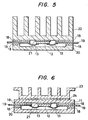
- Figure 5 is a sectional view of a logic LSI package equipped with a heat radiation fin 22 consisting of the electrically insulating sintered body.
- FIG 6 is a sectional view of a logic LSI package equipped with the heat radiation fin 23 made of Al.
- This heat radiation fin 23 is the same as that of Figure 4 except that it was bonded to the SiC sintered body as the substrate 11 by a resin 24.
- a high temperature thermistor having a thermistor constant of 10,000 to 16,000 in the temperature range of 500 to 700°C can be obtained by cutting the SiC sintered body of Example 1 in a suitable size and coating and sintering the paste of the present invention selected from those described in Examples 1 and 2 to form an electrode. Furthermore, a non-linear resistance having a current density of 10 -9 A/c m 2 at room temperature and in an electric field of 1,000 V/cm can be obtained.
Landscapes
- Chemical & Material Sciences (AREA)
- Engineering & Computer Science (AREA)
- Ceramic Engineering (AREA)
- Materials Engineering (AREA)
- Structural Engineering (AREA)
- Organic Chemistry (AREA)
- Parts Printed On Printed Circuit Boards (AREA)
- Ceramic Products (AREA)
- Non-Insulated Conductors (AREA)
- Laminated Bodies (AREA)
Applications Claiming Priority (2)
| Application Number | Priority Date | Filing Date | Title |
|---|---|---|---|
| JP102202/82 | 1982-06-16 | ||
| JP57102202A JPS58223678A (ja) | 1982-06-16 | 1982-06-16 | 金属化層を有するSiC焼結体とその製法 |
Publications (3)
| Publication Number | Publication Date |
|---|---|
| EP0097058A2 true EP0097058A2 (de) | 1983-12-28 |
| EP0097058A3 EP0097058A3 (en) | 1984-10-03 |
| EP0097058B1 EP0097058B1 (de) | 1987-09-30 |
Family
ID=14321076
Family Applications (1)
| Application Number | Title | Priority Date | Filing Date |
|---|---|---|---|
| EP83303456A Expired EP0097058B1 (de) | 1982-06-16 | 1983-06-15 | Gesinterter Gegenstand aus Siliciumcarbid mit metallisierter Schicht und Verfahren zu seiner Herstellung |
Country Status (5)
| Country | Link |
|---|---|
| US (1) | US4663649A (de) |
| EP (1) | EP0097058B1 (de) |
| JP (1) | JPS58223678A (de) |
| KR (1) | KR840005060A (de) |
| DE (1) | DE3373894D1 (de) |
Cited By (4)
| Publication number | Priority date | Publication date | Assignee | Title |
|---|---|---|---|---|
| EP0098067A3 (en) * | 1982-06-16 | 1985-06-12 | Fujitsu Limited | Method for producing multilayered glass-ceramic structure with copper-based conductors therein |
| EP0170012A3 (en) * | 1984-07-06 | 1986-02-12 | Bbc Aktiengesellschaft Brown, Boveri & Cie. | Metal-ceramic composite element and process for its production |
| EP0200469A3 (en) * | 1985-04-25 | 1988-08-03 | Hitachi, Ltd. | Metallizing paste for silicon carbide sintered body and a semiconductor device including the same |
| US5240171A (en) * | 1987-05-21 | 1993-08-31 | Lanxide Technology Company, Lp | Method for surface bonding of ceramic bodies |
Families Citing this family (24)
| Publication number | Priority date | Publication date | Assignee | Title |
|---|---|---|---|---|
| US4784974A (en) * | 1982-08-05 | 1988-11-15 | Olin Corporation | Method of making a hermetically sealed semiconductor casing |
| EP0183016B1 (de) * | 1984-10-03 | 1989-09-20 | Sumitomo Electric Industries Limited | Werkstoff für Halbleiteranordung und Verfahren zu seiner Herstellung |
| DE3784213T2 (de) * | 1986-10-29 | 1993-06-03 | Toshiba Kawasaki Kk | Elektronischer apparat mit einem keramischen substrat. |
| US4731700A (en) * | 1987-02-12 | 1988-03-15 | Delco Electronics Corporation | Semiconductor connection and crossover apparatus |
| US4769345A (en) * | 1987-03-12 | 1988-09-06 | Olin Corporation | Process for producing a hermetically sealed package for an electrical component containing a low amount of oxygen and water vapor |
| JP2548602B2 (ja) * | 1988-04-12 | 1996-10-30 | 株式会社日立製作所 | 半導体実装モジュール |
| US5041695A (en) * | 1989-06-01 | 1991-08-20 | Westinghouse Electric Corp. | Co-fired ceramic package for a power circuit |
| US5169805A (en) * | 1990-01-29 | 1992-12-08 | International Business Machines Corporation | Method of resiliently mounting an integrated circuit chip to enable conformal heat dissipation |
| US5057909A (en) * | 1990-01-29 | 1991-10-15 | International Business Machines Corporation | Electronic device and heat sink assembly |
| US5365108A (en) * | 1992-11-19 | 1994-11-15 | Sundstrand Corporation | Metal matrix composite semiconductor power switch assembly |
| TW363262B (en) * | 1995-10-31 | 1999-07-01 | Nhk Spring Co Ltd | Metallic electronic component packaging arrangement |
| US6388272B1 (en) | 1996-03-07 | 2002-05-14 | Caldus Semiconductor, Inc. | W/WC/TAC ohmic and rectifying contacts on SiC |
| US5929523A (en) * | 1996-03-07 | 1999-07-27 | 3C Semiconductor Corporation | Os rectifying Schottky and ohmic junction and W/WC/TiC ohmic contacts on SiC |
| DE10040591C1 (de) * | 2000-08-15 | 2001-11-08 | Heraeus Gmbh W C | Verfahren zur Herstellung einer Beschichtung auf einem feuerfesten Bauteil und deren Verwendung |
| US7211884B1 (en) | 2002-01-28 | 2007-05-01 | Pacesetter, Inc. | Implantable medical device construction using a flexible substrate |
| US6919504B2 (en) * | 2002-12-19 | 2005-07-19 | 3M Innovative Properties Company | Flexible heat sink |
| US6705393B1 (en) * | 2003-02-25 | 2004-03-16 | Abc Taiwan Electronics Corp. | Ceramic heat sink with micro-pores structure |
| US6849941B1 (en) * | 2004-01-07 | 2005-02-01 | Thermagon, Inc. | Heat sink and heat spreader assembly |
| TWI449137B (zh) * | 2006-03-23 | 2014-08-11 | 製陶技術創新製陶工程股份公司 | 構件或電路用的攜帶體 |
| CN101687716B (zh) * | 2007-04-24 | 2013-11-13 | 陶瓷技术有限责任公司 | 制造敷金属构件的方法、相关构件以及在敷金属过程中用于放置构件的支架 |
| JP2009158725A (ja) * | 2007-12-27 | 2009-07-16 | Panasonic Corp | 半導体装置およびダイボンド材 |
| CN102017107B (zh) | 2008-06-23 | 2013-05-08 | 松下电器产业株式会社 | 接合结构以及电子器件 |
| US10406774B2 (en) * | 2016-10-17 | 2019-09-10 | U.S. Department Of Energy | Diffusion bonding of silicon carbide using iridium and hermetic silicon carbide-iridium bonds |
| JP7148276B2 (ja) * | 2018-05-30 | 2022-10-05 | 京セラ株式会社 | 発光素子搭載用パッケージおよび発光装置 |
Family Cites Families (8)
| Publication number | Priority date | Publication date | Assignee | Title |
|---|---|---|---|---|
| CA615175A (en) * | 1961-02-21 | J. Kroko Leonard | Fused junctions in silicon carbide | |
| NL104185C (de) * | 1957-08-16 | |||
| NL230857A (de) * | 1958-08-26 | |||
| US2937324A (en) * | 1959-02-05 | 1960-05-17 | Westinghouse Electric Corp | Silicon carbide rectifier |
| JPS53130714A (en) * | 1977-04-20 | 1978-11-15 | Kogyo Gijutsuin | Method of bonding nitride base ceramics and silver |
| JPS55143042A (en) * | 1979-04-25 | 1980-11-08 | Hitachi Ltd | Semiconductor device |
| EP0028802B1 (de) * | 1979-11-05 | 1983-08-17 | Hitachi, Ltd. | Elektrisch isolierendes Substrat und Verfahren zur Herstellung eines solchen Substrats |
| JPS58101442A (ja) * | 1981-12-11 | 1983-06-16 | Hitachi Ltd | 電気的装置用基板 |
-
1982
- 1982-06-16 JP JP57102202A patent/JPS58223678A/ja active Granted
-
1983
- 1983-06-15 DE DE8383303456T patent/DE3373894D1/de not_active Expired
- 1983-06-15 EP EP83303456A patent/EP0097058B1/de not_active Expired
- 1983-06-16 KR KR1019830002696A patent/KR840005060A/ko not_active Withdrawn
- 1983-06-16 US US06/504,787 patent/US4663649A/en not_active Expired - Fee Related
Cited By (5)
| Publication number | Priority date | Publication date | Assignee | Title |
|---|---|---|---|---|
| EP0098067A3 (en) * | 1982-06-16 | 1985-06-12 | Fujitsu Limited | Method for producing multilayered glass-ceramic structure with copper-based conductors therein |
| EP0170012A3 (en) * | 1984-07-06 | 1986-02-12 | Bbc Aktiengesellschaft Brown, Boveri & Cie. | Metal-ceramic composite element and process for its production |
| CH660176A5 (de) * | 1984-07-06 | 1987-03-31 | Bbc Brown Boveri & Cie | Metall-keramik-verbundelement und verfahren zu dessen herstellung. |
| EP0200469A3 (en) * | 1985-04-25 | 1988-08-03 | Hitachi, Ltd. | Metallizing paste for silicon carbide sintered body and a semiconductor device including the same |
| US5240171A (en) * | 1987-05-21 | 1993-08-31 | Lanxide Technology Company, Lp | Method for surface bonding of ceramic bodies |
Also Published As
| Publication number | Publication date |
|---|---|
| EP0097058A3 (en) | 1984-10-03 |
| EP0097058B1 (de) | 1987-09-30 |
| US4663649A (en) | 1987-05-05 |
| KR840005060A (ko) | 1984-11-03 |
| DE3373894D1 (en) | 1987-11-05 |
| JPS58223678A (ja) | 1983-12-26 |
| JPS6230159B2 (de) | 1987-06-30 |
Similar Documents
| Publication | Publication Date | Title |
|---|---|---|
| EP0097058B1 (de) | Gesinterter Gegenstand aus Siliciumcarbid mit metallisierter Schicht und Verfahren zu seiner Herstellung | |
| US4961987A (en) | Aluminum nitride sintered body with high thermal conductivity and process for producing same | |
| EP0153737B1 (de) | Schaltungssubstrat mit hoher Wärmeleitfähigkeit | |
| US4517584A (en) | Ceramic packaged semiconductor device | |
| US5164246A (en) | Highly thermoconductive ceramic | |
| JPS631267B2 (de) | ||
| EP0200469B1 (de) | Metallisierungspaste für Siliziumcarbidkörper und diese Paste enthaltendes Halbleitergerät | |
| JP2578283B2 (ja) | 窒化アルミニウム基板のメタライズ方法 | |
| JPS61281089A (ja) | 窒化アルミニウム製基材の表面構造 | |
| JP3538549B2 (ja) | 配線基板およびその製造方法 | |
| JPH0576795B2 (de) | ||
| JPH05226515A (ja) | メタライズ層を有する窒化アルミニウム基板とそのメタライズ方法 | |
| EP0200950B1 (de) | Eutektische Zusammensetzung enthaltende Paste, Verfahren zu deren Bildung und deren Anwendung | |
| JPH05170552A (ja) | メタライズ層を有する窒化アルミニウム基板とそのメタライズ方法 | |
| JPH0313190B2 (de) | ||
| JPH05221759A (ja) | メタライズ層を有する窒化アルミニウム基板とそのメタライズ方法 | |
| JPH04290488A (ja) | 非酸化物系セラミックス回路基板の製法および該基板を用いた電子装置の製法 | |
| JP2763516B2 (ja) | 窒化アルミニウム基板のメタライズ方法 | |
| JPS61281074A (ja) | メタライズ用高熱伝導性窒化アルミニウム焼結体 | |
| JP2704158B2 (ja) | 導電性メタライズ層を有する窒化アルミニウム焼結体およびその製造方法 | |
| JPH0619926B2 (ja) | 回路基板とその製法 | |
| WO2026058762A1 (ja) | 焼結性接合用ペースト及び接合構造体 | |
| JPH0723273B2 (ja) | 窒化アルミニウム基板のメタライズ方法 | |
| JPS62197376A (ja) | 窒化アルミニウム基板 | |
| JPS62108786A (ja) | 金属化窒化アルミニウム体及びその製法 |
Legal Events
| Date | Code | Title | Description |
|---|---|---|---|
| PUAI | Public reference made under article 153(3) epc to a published international application that has entered the european phase |
Free format text: ORIGINAL CODE: 0009012 |
|
| 17P | Request for examination filed |
Effective date: 19830729 |
|
| AK | Designated contracting states |
Designated state(s): CH DE FR GB IT LI NL SE |
|
| PUAL | Search report despatched |
Free format text: ORIGINAL CODE: 0009013 |
|
| AK | Designated contracting states |
Designated state(s): CH DE FR GB IT LI NL SE |
|
| GRAA | (expected) grant |
Free format text: ORIGINAL CODE: 0009210 |
|
| RBV | Designated contracting states (corrected) |
Designated state(s): DE FR GB |
|
| AK | Designated contracting states |
Kind code of ref document: B1 Designated state(s): DE FR GB |
|
| REF | Corresponds to: |
Ref document number: 3373894 Country of ref document: DE Date of ref document: 19871105 |
|
| ET | Fr: translation filed | ||
| PLBE | No opposition filed within time limit |
Free format text: ORIGINAL CODE: 0009261 |
|
| STAA | Information on the status of an ep patent application or granted ep patent |
Free format text: STATUS: NO OPPOSITION FILED WITHIN TIME LIMIT |
|
| 26N | No opposition filed | ||
| PGFP | Annual fee paid to national office [announced via postgrant information from national office to epo] |
Ref country code: GB Payment date: 19980608 Year of fee payment: 16 |
|
| PG25 | Lapsed in a contracting state [announced via postgrant information from national office to epo] |
Ref country code: GB Free format text: LAPSE BECAUSE OF NON-PAYMENT OF DUE FEES Effective date: 19990615 |
|
| GBPC | Gb: european patent ceased through non-payment of renewal fee |
Effective date: 19990615 |
|
| PGFP | Annual fee paid to national office [announced via postgrant information from national office to epo] |
Ref country code: DE Payment date: 20000824 Year of fee payment: 18 |
|
| PGFP | Annual fee paid to national office [announced via postgrant information from national office to epo] |
Ref country code: FR Payment date: 20010619 Year of fee payment: 19 |
|
| PG25 | Lapsed in a contracting state [announced via postgrant information from national office to epo] |
Ref country code: DE Free format text: LAPSE BECAUSE OF NON-PAYMENT OF DUE FEES Effective date: 20020403 |
|
| PG25 | Lapsed in a contracting state [announced via postgrant information from national office to epo] |
Ref country code: FR Free format text: LAPSE BECAUSE OF NON-PAYMENT OF DUE FEES Effective date: 20030228 |
|
| REG | Reference to a national code |
Ref country code: FR Ref legal event code: ST |