EP0097304A2 - Tube de faisceau d'électrons plat avec décharge dans les gaz pour source d'électrons - Google Patents
Tube de faisceau d'électrons plat avec décharge dans les gaz pour source d'électrons Download PDFInfo
- Publication number
- EP0097304A2 EP0097304A2 EP83105788A EP83105788A EP0097304A2 EP 0097304 A2 EP0097304 A2 EP 0097304A2 EP 83105788 A EP83105788 A EP 83105788A EP 83105788 A EP83105788 A EP 83105788A EP 0097304 A2 EP0097304 A2 EP 0097304A2
- Authority
- EP
- European Patent Office
- Prior art keywords
- electron
- openings
- conductors
- gas discharge
- column
- Prior art date
- Legal status (The legal status is an assumption and is not a legal conclusion. Google has not performed a legal analysis and makes no representation as to the accuracy of the status listed.)
- Granted
Links
- 238000010894 electron beam technology Methods 0.000 title claims description 11
- 239000004020 conductor Substances 0.000 claims abstract description 65
- 238000006073 displacement reaction Methods 0.000 claims 1
- 239000011159 matrix material Substances 0.000 abstract description 15
- 150000002500 ions Chemical class 0.000 abstract description 11
- 230000000694 effects Effects 0.000 description 5
- 230000001133 acceleration Effects 0.000 description 4
- 239000002800 charge carrier Substances 0.000 description 3
- 238000004519 manufacturing process Methods 0.000 description 3
- 239000011521 glass Substances 0.000 description 2
- 239000000463 material Substances 0.000 description 2
- 230000005855 radiation Effects 0.000 description 2
- 125000006850 spacer group Chemical group 0.000 description 2
- OAICVXFJPJFONN-UHFFFAOYSA-N Phosphorus Chemical compound [P] OAICVXFJPJFONN-UHFFFAOYSA-N 0.000 description 1
- 238000006243 chemical reaction Methods 0.000 description 1
- 238000010276 construction Methods 0.000 description 1
- 230000007423 decrease Effects 0.000 description 1
- 238000011161 development Methods 0.000 description 1
- 230000018109 developmental process Effects 0.000 description 1
- 238000010586 diagram Methods 0.000 description 1
- 238000009826 distribution Methods 0.000 description 1
- 238000002474 experimental method Methods 0.000 description 1
- 230000002349 favourable effect Effects 0.000 description 1
- 230000009931 harmful effect Effects 0.000 description 1
- 230000002452 interceptive effect Effects 0.000 description 1
- 238000000034 method Methods 0.000 description 1
- 239000000203 mixture Substances 0.000 description 1
- 230000003287 optical effect Effects 0.000 description 1
- 238000005192 partition Methods 0.000 description 1
- 230000035515 penetration Effects 0.000 description 1
- 239000007787 solid Substances 0.000 description 1
- 230000001360 synchronised effect Effects 0.000 description 1
Images
Classifications
-
- H—ELECTRICITY
- H01—ELECTRIC ELEMENTS
- H01J—ELECTRIC DISCHARGE TUBES OR DISCHARGE LAMPS
- H01J17/00—Gas-filled discharge tubes with solid cathode
- H01J17/38—Cold-cathode tubes
- H01J17/48—Cold-cathode tubes with more than one cathode or anode, e.g. sequence-discharge tube, counting tube, dekatron
- H01J17/49—Display panels, e.g. with crossed electrodes, e.g. making use of direct current
- H01J17/498—Display panels, e.g. with crossed electrodes, e.g. making use of direct current with a gas discharge space and a post acceleration space for electrons
Definitions
- the invention relates to an electron tube according to the preamble of claim 1.
- Such a flat screen is described for example in DE-PS 24 12 869.
- This flat display has already been developed to such an extent that it delivers (color) television images in the laboratory with perfectly acceptable optical qualities. If you haven't gotten far beyond the laboratory stage so that the laboratory has progressed, it is mainly due to some plasma-related problems, Les 1 Lk / May 24, 1982
- the invention is based on the object of modifying a two-chamber display of the type mentioned at the outset in such a way that it becomes puncture-resistant, no longer has annoying underground lighting and can be produced rationally, even then , if the display should have a high resolution.
- a control plate designed according to the invention appears opaque in plan view, since the openings on f on one side of the plate are covered by webs on the other side of the plate; it is accordingly clear that this disk does not pass ultraviolet or visible radiation from the plasma at any point.
- the fact that the control plate with its curved passage channels also intercepts interfering charge carriers is less obvious, for Mutzelek- is permeable. This discriminator effect, which has already been fully confirmed in the experiment, can be explained as follows: The useful electrons, that is to say the plasma electrons focused on the line being driven, are relatively slow.
- the opposite web of the deflection fields located there is at a sufficiently negative potential - deflected to the side, for the most part so far that they get sucked into the acceleration field reaching through the column openings and thus be pulled into the post-acceleration space overall on a curved path.
- the potential ratios can be selected such that only relatively few useful electrons flying through the center of the inlet opening are intercepted by the web. The majority of the fast electrons, on the other hand, experience this fate, the orbits of which are naturally "stiff" and can only be slightly bent by the deflection fields.
- the decoupling achieved with the concealed control disc is so good that considerable freedom has been regained in the choice of the gas mixture and the gas pressure as well as in the design of the cathode.
- the fact that the electron beams entering the post-acceleration space are already very well bundled is also favorable, so that at most a simple refocusing is required in order to unite associated sub-beams again into a single beam with a small cross-section.
- the line openings are enlarged. and thus increase the electron yield without having to accept dangerous voltage penetrations.
- the display design proposed here has a control characteristic that, particularly if you want to generate the grayscale by means of pulse length modulation, makes it much easier to maintain uniform image brightness everywhere: the screen current flows into an increasing control voltage practically constant plateau over wide voltage ranges.
- each column conductor should have an electron-optical cylindrical lens assigned to it.
- Such a lens which on the one hand provides for refocusing and on the other hand shields the individual column conductors from one another, can be implemented in individual cases by one or two column-parallel conductor tracks per column conductor.
- a control disk in which the column-side and the row-side openings are not in alignment with one another is already known from DE-OS 30 10 179.
- this proposal which is only intended to make production easier, is based on the holes at least partially overlapping, so that the harmful effects between the two spaces are essentially not dampened at all.
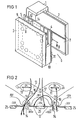
- the flat screen of FIG. 1 contains in particular a gas-filled cover 1 with a back plate 2 and a front plate 3 and a control plate 4. All three plates lie in mutually parallel planes, the control plate dividing the inside of the cover into two rooms, a front acceleration chamber 5 and one rear gas discharge space 6, divided.
- the back plate 2 is provided on its front side with a family of parallel, relatively large-area cathode strips 7.
- the front plate 3 carries on its back a regular grid of phosphor points 8, which can be excited by electrons to emit light, and above it a post-acceleration anode 9.
- the control plate 4, which is supported against the front plate 3 by a spacer frame 10, contains one on the back Family of row conductors 11 parallel to one another and column side 12 on their front side.
- the row conductors run parallel to the cathode strips 7 and the column conductors extend perpendicularly thereto. Openings - electron entry openings 13 in the row conductors 11 and electron exit openings 1L in the column conductors 12 - are introduced into each of the conductors 11, 12.
- the following voltages are present on the individual electrodes: on the selected and non-selected cathode strips 7-200V or 0V; on the keyed and non-keyed row conductors 11 OV or -50V; on the column conductors 12 between -80V and -30V; and at the post-acceleration anode 9 ⁇ 4kV.
- the electrode matrix is addressed line sequentially, and the cathode voltages are synchronized with the line scanning voltage in such a way that the plasma burns between the selected line conductor and the cathode strip just opposite. Further details of this control principle can be found in DE-OS 26 43915. For the rest, reference is made to the one already cited DE-PS 24 12 869 referenced, which among other things also deals extensively with questions of construction.
- the control plate 4 acts in a viewing direction perpendicular to the plate extension like a continuous disc, since its openings on one side are covered by solid panels on the other side.
- essentially only the conductor part of the entire plate 4 is drawn in; only the column supports 25, which close the gaps between the column conductors, are indicated by the structure carrying the conductors, which close the gaps between the column conductors.
- the row conductors 11 are 340 ⁇ m wide and 60 ⁇ m apart
- the electron entry openings 13 are rectangles with an area of 220 x 200 ⁇ m - the narrow sides run parallel to the row conductor extension - and are each 200 ⁇ m apart.
- the column conductors are 340 ⁇ m wide, hold one Also at a distance of 60 ⁇ m from one another and have slot-shaped electron exit openings 14. These slots, which run parallel to the column conductor extension, are 300 ⁇ m long, 80 ⁇ m wide and are each placed behind one of the row conductor webs that remain between adjacent electron entry openings.
- the control plate 4 which is shown in FIG. 1 for the sake of simplicity as an unstructured block, is to be designed in practice in such a way that on the one hand it can function as a stable support for the row and column conductors and on the other hand it contains electron passage channels which the connect mutually associated electron openings.
- the production of such a support structure does not pose any fundamental difficulties in practice since it is possible to use techniques which have already been developed for control disks with straight openings. So you could first of all the row and column conductors on a thin glass film shape and then etch the glass through the conductor openings down to relatively small-area joints between the two sets of conductors.
- a second possibility is to first implement the row and column conductors on separate support systems and then to assemble these units in the correct position relative to one another.
- the support systems will contain mutually parallel insulating webs, each of which is positioned between two adjacent conductors and possibly completed by a few cross struts to form a self-supporting structure.
- FIG. 2 shows the potential relationships in the region of the electrode matrix, specifically in the event that the row conductor is selected and the column conductors are at pass potential. If you select the row conductor voltage as the reference potential, the column conductors are at - 30V. If one also adds the influences from the gas discharge space on the one hand and the post-acceleration space on the other, a potential distribution results, of which some characteristic equipotential surfaces are drawn in the diagram and provided with the associated potential values. Two saddle points of -5V can be seen, one approximately in the center of the electron beam entry opening and another above the electron beam exit opening. According to the electron-optical laws, opening.
- the saddle point on the line conductor side which has a more positive potential than the potential area generating it, has a dispersing effect for electrons and for collecting ions, while the saddle point above the column opening, which is formed by a potential area with a more positive potential, collects the electrons and that Ions scattered.
- These two lens effects change the trajectories of the charge carriers entering the control chamber in a characteristic manner.
- representative trajectories of electrons curves 15, 16 and 17
- ions curves 13 and 19
- Curves 15 and 16 belong to slow electrons from the gas discharge, curve 17 denotes the path of a fast plasma electron and curves 18 and 19 describe the paths of a fast or decelerated ion from the post-acceleration space. It can be seen that the low-energy electrons are drawn through the control chamber on a curved path and enter the post-acceleration chamber as a relatively well focused beam. The slow ions are first scattered and then - under the influence of a constantly moving field - transported to the inside of the column conductors. The fast electrons and ions are only slightly deflected by the relatively weak fields; they burst onto the parts of the control structure that act as panels and are largely made harmless.
- the invention is of course not limited to the illustrated embodiment. This means that there is still considerable scope for design, especially when designing the control disc. The only important thing is to set the openings on both sides of the control disc "on gap" with each other. For example, one could move the openings of the even-numbered row conductors and allow the column conductors to run correspondingly in a zigzag shape (cf. also DE-PS 26 15 569).
- each column conductor is flanked by one or two additional letters, to apply these intermediate electrodes as parallel strips on the front of an insulating rod and to fix the rod on the back with two adjacent column conductors.
Landscapes
- Gas-Filled Discharge Tubes (AREA)
- Lasers (AREA)
- Analysing Materials By The Use Of Radiation (AREA)
- Cathode-Ray Tubes And Fluorescent Screens For Display (AREA)
Priority Applications (1)
| Application Number | Priority Date | Filing Date | Title |
|---|---|---|---|
| AT83105788T ATE26504T1 (de) | 1982-06-18 | 1983-06-13 | Flache elektronenstrahlroehre mit einer gasentladung als elektronenquelle. |
Applications Claiming Priority (2)
| Application Number | Priority Date | Filing Date | Title |
|---|---|---|---|
| DE19823222850 DE3222850A1 (de) | 1982-06-18 | 1982-06-18 | Flache elektronenstrahlroehre mit einer gasentladung als elektronenquelle |
| DE3222850 | 1982-06-18 |
Publications (3)
| Publication Number | Publication Date |
|---|---|
| EP0097304A2 true EP0097304A2 (fr) | 1984-01-04 |
| EP0097304A3 EP0097304A3 (en) | 1984-10-17 |
| EP0097304B1 EP0097304B1 (fr) | 1987-04-08 |
Family
ID=6166311
Family Applications (1)
| Application Number | Title | Priority Date | Filing Date |
|---|---|---|---|
| EP83105788A Expired EP0097304B1 (fr) | 1982-06-18 | 1983-06-13 | Tube de faisceau d'électrons plat avec décharge dans les gaz pour source d'électrons |
Country Status (5)
| Country | Link |
|---|---|
| US (1) | US4564790A (fr) |
| EP (1) | EP0097304B1 (fr) |
| JP (1) | JPS598250A (fr) |
| AT (1) | ATE26504T1 (fr) |
| DE (2) | DE3222850A1 (fr) |
Cited By (1)
| Publication number | Priority date | Publication date | Assignee | Title |
|---|---|---|---|---|
| EP0167930A1 (fr) * | 1984-07-02 | 1986-01-15 | Nokia Graetz Gesellschaft mit beschränkter Haftung | Dispositif de contrôle d'électrons pour appareils d'affichage à décharge à gaz |
Families Citing this family (11)
| Publication number | Priority date | Publication date | Assignee | Title |
|---|---|---|---|---|
| DE3228183C2 (de) * | 1982-07-28 | 1984-08-30 | Siemens AG, 1000 Berlin und 8000 München | Flache Elektronenstrahlröhre und Verfahren zu ihrer Herstellung |
| DE3406252A1 (de) * | 1984-02-21 | 1985-08-22 | Siemens AG, 1000 Berlin und 8000 München | Flache gasentladungsanzeigevorrichtung |
| US4719388A (en) * | 1985-08-13 | 1988-01-12 | Source Technology Corporation | Flat electron control device utilizing a uniform space-charge cloud of free electrons as a virtual cathode |
| DE3911346A1 (de) * | 1989-04-07 | 1990-10-11 | Nokia Unterhaltungselektronik | Steuersystem fuer flache bildwiedergabevorrichtungen |
| DE3911343A1 (de) * | 1989-04-07 | 1990-10-11 | Nokia Unterhaltungselektronik | Flache anzeigeeinrichtung |
| US5256937A (en) * | 1989-04-07 | 1993-10-26 | Nokia (Deutschland) Gmbh | Flat panel fluorescent screen display tube |
| US5386175A (en) * | 1990-05-24 | 1995-01-31 | U.S. Philips Corporation | Thin-type picture display device |
| US5477105A (en) * | 1992-04-10 | 1995-12-19 | Silicon Video Corporation | Structure of light-emitting device with raised black matrix for use in optical devices such as flat-panel cathode-ray tubes |
| US5424605A (en) * | 1992-04-10 | 1995-06-13 | Silicon Video Corporation | Self supporting flat video display |
| US5686790A (en) * | 1993-06-22 | 1997-11-11 | Candescent Technologies Corporation | Flat panel device with ceramic backplate |
| US5407210A (en) * | 1993-11-15 | 1995-04-18 | Canning; Robert P. | Portable game apparatus for playing curb ball or other ball game |
Family Cites Families (10)
| Publication number | Priority date | Publication date | Assignee | Title |
|---|---|---|---|---|
| US3845241A (en) * | 1973-02-02 | 1974-10-29 | Zenith Radio Corp | Television display panel having gas discharge cathodo-luminescent elements |
| DE2412869C3 (de) * | 1974-03-18 | 1980-10-30 | Siemens Ag, 1000 Berlin Und 8000 Muenchen | Anzeigevorrichtung mit einem Gasentladungsraum als Elektronenquelle, mit einem Elektronennachbeschleunigungsraum und mit einem Leuchtschirm und Verfahren zum Betrieb dieser Anzeigevorrichtung |
| DE2615569C3 (de) * | 1976-04-09 | 1982-01-14 | Siemens AG, 1000 Berlin und 8000 München | Farbbildwiedergabevorrichtung |
| DE2643915C2 (de) * | 1976-09-29 | 1983-10-06 | Siemens Ag, 1000 Berlin Und 8000 Muenchen | Anzeigevorrichtung |
| US4236096A (en) * | 1976-12-14 | 1980-11-25 | Siemens Aktiengesellschaft | Plasma image display device |
| DE2656621C3 (de) * | 1976-12-14 | 1980-08-14 | Siemens Ag, 1000 Berlin Und 8000 Muenchen | Bildanzeigevorrichtung mit einer Gasentladungsstrecke und einer Elektronenbeschleunigungsstrecke |
| DE2855056C2 (de) * | 1978-12-20 | 1982-04-15 | Siemens AG, 1000 Berlin und 8000 München | Gasentladungsanzeigevorrichtung |
| DE2926393C2 (de) * | 1979-06-29 | 1982-10-07 | Siemens AG, 1000 Berlin und 8000 München | Gasentladungsanzeigevorrichtung |
| DE3010179A1 (de) * | 1980-03-17 | 1981-09-24 | Siemens AG, 1000 Berlin und 8000 München | Steuerscheibe fuer einen flachen plasmabildschirm |
| US4376258A (en) * | 1981-04-16 | 1983-03-08 | Rca Corporation | Shielded beam guide structure for a flat panel display device and method of making same |
-
1982
- 1982-06-18 DE DE19823222850 patent/DE3222850A1/de not_active Withdrawn
-
1983
- 1983-06-13 AT AT83105788T patent/ATE26504T1/de not_active IP Right Cessation
- 1983-06-13 DE DE8383105788T patent/DE3370896D1/de not_active Expired
- 1983-06-13 EP EP83105788A patent/EP0097304B1/fr not_active Expired
- 1983-06-16 JP JP58108536A patent/JPS598250A/ja active Pending
- 1983-06-17 US US06/505,308 patent/US4564790A/en not_active Expired - Fee Related
Cited By (1)
| Publication number | Priority date | Publication date | Assignee | Title |
|---|---|---|---|---|
| EP0167930A1 (fr) * | 1984-07-02 | 1986-01-15 | Nokia Graetz Gesellschaft mit beschränkter Haftung | Dispositif de contrôle d'électrons pour appareils d'affichage à décharge à gaz |
Also Published As
| Publication number | Publication date |
|---|---|
| DE3222850A1 (de) | 1983-12-22 |
| EP0097304A3 (en) | 1984-10-17 |
| JPS598250A (ja) | 1984-01-17 |
| EP0097304B1 (fr) | 1987-04-08 |
| US4564790A (en) | 1986-01-14 |
| DE3370896D1 (en) | 1987-05-14 |
| ATE26504T1 (de) | 1987-04-15 |
Similar Documents
| Publication | Publication Date | Title |
|---|---|---|
| DE2412869C3 (de) | Anzeigevorrichtung mit einem Gasentladungsraum als Elektronenquelle, mit einem Elektronennachbeschleunigungsraum und mit einem Leuchtschirm und Verfahren zum Betrieb dieser Anzeigevorrichtung | |
| DE2642674C2 (de) | Elektronenstrahl-Wiedergabeeinrichtung | |
| DE2418199C2 (de) | Farbbildwiedergabeanordnung | |
| DE2902852C2 (de) | Flache Elektronenstrahl-Bildwiedergaberöhre | |
| DE2615721A1 (de) | Gasentladungsanzeigevorrichtung | |
| EP0097304B1 (fr) | Tube de faisceau d'électrons plat avec décharge dans les gaz pour source d'électrons | |
| DE3910005A1 (de) | Bildanzeigegeraet | |
| DE3115890C2 (de) | Gasentladungs-Anzeigevorrichtung | |
| DE2724122A1 (de) | Elektronenwiedergabeeinrichtung | |
| EP0061525A1 (fr) | Tube de reproduction d'image plat | |
| EP0109010A2 (fr) | Dispositif plat de reproduction d'images | |
| DE1098030B (de) | Farbfernseh-Bildroehre | |
| DE2656621C3 (de) | Bildanzeigevorrichtung mit einer Gasentladungsstrecke und einer Elektronenbeschleunigungsstrecke | |
| DE2811355A1 (de) | Geraet mit einer kathodenstrahlroehre | |
| DE3035241A1 (de) | Farbbildwiedergaberoehre und vorrichtung mit einer derartigen roehre | |
| DE2926393C2 (de) | Gasentladungsanzeigevorrichtung | |
| EP0012922B1 (fr) | Dispositif d'affichage à décharge à gaz | |
| DE1098628B (de) | Indikatorroehre zur Projektion von Ziffern und Buchstaben fuer Zaehl- und Rechenmaschinen | |
| EP0017981A1 (fr) | Dispositif d'affichage à décharge dans un gaz à cathode de profilée | |
| DE2944100A1 (de) | Bildwiedergabegeraet in flachbauweise mit strahlkollektor | |
| DE3529041A1 (de) | Flache, hochaufloesende bildanzeigevorrichtung | |
| DE3334327A1 (de) | Farbauswahl-elektronenstrahlfuehrungsanordnung fuer flache anzeige- und bildwiedergabegeraete | |
| DE3406252A1 (de) | Flache gasentladungsanzeigevorrichtung | |
| DE3328884A1 (de) | Kathodenstrahlroehre mit vierpolig fokussierender farbwahleinrichtung | |
| DE3138955A1 (de) | Gasentladungsanzeigevorrichtung mit nahfokussierung |
Legal Events
| Date | Code | Title | Description |
|---|---|---|---|
| PUAI | Public reference made under article 153(3) epc to a published international application that has entered the european phase |
Free format text: ORIGINAL CODE: 0009012 |
|
| AK | Designated contracting states |
Designated state(s): AT CH DE FR GB IT LI NL SE |
|
| PUAL | Search report despatched |
Free format text: ORIGINAL CODE: 0009013 |
|
| AK | Designated contracting states |
Designated state(s): AT CH DE FR GB IT LI NL SE |
|
| 17P | Request for examination filed |
Effective date: 19841114 |
|
| GRAA | (expected) grant |
Free format text: ORIGINAL CODE: 0009210 |
|
| AK | Designated contracting states |
Kind code of ref document: B1 Designated state(s): AT CH DE FR GB IT LI NL SE |
|
| REF | Corresponds to: |
Ref document number: 26504 Country of ref document: AT Date of ref document: 19870415 Kind code of ref document: T |
|
| REF | Corresponds to: |
Ref document number: 3370896 Country of ref document: DE Date of ref document: 19870514 |
|
| ET | Fr: translation filed | ||
| PG25 | Lapsed in a contracting state [announced via postgrant information from national office to epo] |
Ref country code: AT Effective date: 19870613 |
|
| PG25 | Lapsed in a contracting state [announced via postgrant information from national office to epo] |
Ref country code: SE Effective date: 19870614 |
|
| ITF | It: translation for a ep patent filed | ||
| PG25 | Lapsed in a contracting state [announced via postgrant information from national office to epo] |
Ref country code: LI Effective date: 19870630 Ref country code: CH Effective date: 19870630 |
|
| PG25 | Lapsed in a contracting state [announced via postgrant information from national office to epo] |
Ref country code: NL Effective date: 19880101 |
|
| NLV4 | Nl: lapsed or anulled due to non-payment of the annual fee | ||
| PG25 | Lapsed in a contracting state [announced via postgrant information from national office to epo] |
Ref country code: FR Free format text: LAPSE BECAUSE OF NON-PAYMENT OF DUE FEES Effective date: 19880226 |
|
| REG | Reference to a national code |
Ref country code: CH Ref legal event code: PL |
|
| PG25 | Lapsed in a contracting state [announced via postgrant information from national office to epo] |
Ref country code: DE Effective date: 19880301 |
|
| GBPC | Gb: european patent ceased through non-payment of renewal fee | ||
| PLBE | No opposition filed within time limit |
Free format text: ORIGINAL CODE: 0009261 |
|
| STAA | Information on the status of an ep patent application or granted ep patent |
Free format text: STATUS: NO OPPOSITION FILED WITHIN TIME LIMIT |
|
| REG | Reference to a national code |
Ref country code: FR Ref legal event code: ST |
|
| 26N | No opposition filed | ||
| PG25 | Lapsed in a contracting state [announced via postgrant information from national office to epo] |
Ref country code: GB Effective date: 19881122 |
|
| EUG | Se: european patent has lapsed |
Ref document number: 83105788.0 Effective date: 19880713 |