EP0097326B1 - Halbleiteranordnung mit Wannenstruktur - Google Patents
Halbleiteranordnung mit Wannenstruktur Download PDFInfo
- Publication number
- EP0097326B1 EP0097326B1 EP83105880A EP83105880A EP0097326B1 EP 0097326 B1 EP0097326 B1 EP 0097326B1 EP 83105880 A EP83105880 A EP 83105880A EP 83105880 A EP83105880 A EP 83105880A EP 0097326 B1 EP0097326 B1 EP 0097326B1
- Authority
- EP
- European Patent Office
- Prior art keywords
- layer
- semiconductor device
- disposed
- impurity region
- impurity
- Prior art date
- Legal status (The legal status is an assumption and is not a legal conclusion. Google has not performed a legal analysis and makes no representation as to the accuracy of the status listed.)
- Expired
Links
Images


Classifications
-
- H—ELECTRICITY
- H10—SEMICONDUCTOR DEVICES; ELECTRIC SOLID-STATE DEVICES NOT OTHERWISE PROVIDED FOR
- H10D—INORGANIC ELECTRIC SEMICONDUCTOR DEVICES
- H10D84/00—Integrated devices formed in or on semiconductor substrates that comprise only semiconducting layers, e.g. on Si wafers or on GaAs-on-Si wafers
- H10D84/01—Manufacture or treatment
- H10D84/0123—Integrating together multiple components covered by H10D12/00 or H10D30/00, e.g. integrating multiple IGBTs
- H10D84/0126—Integrating together multiple components covered by H10D12/00 or H10D30/00, e.g. integrating multiple IGBTs the components including insulated gates, e.g. IGFETs
- H10D84/0156—Manufacturing their doped wells
-
- H—ELECTRICITY
- H10—SEMICONDUCTOR DEVICES; ELECTRIC SOLID-STATE DEVICES NOT OTHERWISE PROVIDED FOR
- H10W—GENERIC PACKAGES, INTERCONNECTIONS, CONNECTORS OR OTHER CONSTRUCTIONAL DETAILS OF DEVICES COVERED BY CLASS H10
- H10W10/00—Isolation regions in semiconductor bodies between components of integrated devices
- H10W10/01—Manufacture or treatment
- H10W10/011—Manufacture or treatment of isolation regions comprising dielectric materials
- H10W10/014—Manufacture or treatment of isolation regions comprising dielectric materials using trench refilling with dielectric materials, e.g. shallow trench isolations
-
- H—ELECTRICITY
- H10—SEMICONDUCTOR DEVICES; ELECTRIC SOLID-STATE DEVICES NOT OTHERWISE PROVIDED FOR
- H10D—INORGANIC ELECTRIC SEMICONDUCTOR DEVICES
- H10D30/00—Field-effect transistors [FET]
- H10D30/60—Insulated-gate field-effect transistors [IGFET]
-
- H—ELECTRICITY
- H10—SEMICONDUCTOR DEVICES; ELECTRIC SOLID-STATE DEVICES NOT OTHERWISE PROVIDED FOR
- H10D—INORGANIC ELECTRIC SEMICONDUCTOR DEVICES
- H10D84/00—Integrated devices formed in or on semiconductor substrates that comprise only semiconducting layers, e.g. on Si wafers or on GaAs-on-Si wafers
- H10D84/01—Manufacture or treatment
- H10D84/0123—Integrating together multiple components covered by H10D12/00 or H10D30/00, e.g. integrating multiple IGBTs
- H10D84/0126—Integrating together multiple components covered by H10D12/00 or H10D30/00, e.g. integrating multiple IGBTs the components including insulated gates, e.g. IGFETs
- H10D84/0151—Manufacturing their isolation regions
-
- H—ELECTRICITY
- H10—SEMICONDUCTOR DEVICES; ELECTRIC SOLID-STATE DEVICES NOT OTHERWISE PROVIDED FOR
- H10D—INORGANIC ELECTRIC SEMICONDUCTOR DEVICES
- H10D84/00—Integrated devices formed in or on semiconductor substrates that comprise only semiconducting layers, e.g. on Si wafers or on GaAs-on-Si wafers
- H10D84/80—Integrated devices formed in or on semiconductor substrates that comprise only semiconducting layers, e.g. on Si wafers or on GaAs-on-Si wafers characterised by the integration of at least one component covered by groups H10D12/00 or H10D30/00, e.g. integration of IGFETs
- H10D84/82—Integrated devices formed in or on semiconductor substrates that comprise only semiconducting layers, e.g. on Si wafers or on GaAs-on-Si wafers characterised by the integration of at least one component covered by groups H10D12/00 or H10D30/00, e.g. integration of IGFETs of only field-effect components
- H10D84/83—Integrated devices formed in or on semiconductor substrates that comprise only semiconducting layers, e.g. on Si wafers or on GaAs-on-Si wafers characterised by the integration of at least one component covered by groups H10D12/00 or H10D30/00, e.g. integration of IGFETs of only field-effect components of only insulated-gate FETs [IGFET]
- H10D84/85—Complementary IGFETs, e.g. CMOS
- H10D84/854—Complementary IGFETs, e.g. CMOS comprising arrangements for preventing bipolar actions between the different IGFET regions, e.g. arrangements for latchup prevention
-
- H—ELECTRICITY
- H10—SEMICONDUCTOR DEVICES; ELECTRIC SOLID-STATE DEVICES NOT OTHERWISE PROVIDED FOR
- H10W—GENERIC PACKAGES, INTERCONNECTIONS, CONNECTORS OR OTHER CONSTRUCTIONAL DETAILS OF DEVICES COVERED BY CLASS H10
- H10W10/00—Isolation regions in semiconductor bodies between components of integrated devices
- H10W10/01—Manufacture or treatment
- H10W10/011—Manufacture or treatment of isolation regions comprising dielectric materials
- H10W10/012—Manufacture or treatment of isolation regions comprising dielectric materials using local oxidation of silicon [LOCOS]
-
- H—ELECTRICITY
- H10—SEMICONDUCTOR DEVICES; ELECTRIC SOLID-STATE DEVICES NOT OTHERWISE PROVIDED FOR
- H10W—GENERIC PACKAGES, INTERCONNECTIONS, CONNECTORS OR OTHER CONSTRUCTIONAL DETAILS OF DEVICES COVERED BY CLASS H10
- H10W10/00—Isolation regions in semiconductor bodies between components of integrated devices
- H10W10/10—Isolation regions comprising dielectric materials
- H10W10/13—Isolation regions comprising dielectric materials formed using local oxidation of silicon [LOCOS], e.g. sealed interface localised oxidation [SILO] or side-wall mask isolation [SWAMI]
-
- H—ELECTRICITY
- H10—SEMICONDUCTOR DEVICES; ELECTRIC SOLID-STATE DEVICES NOT OTHERWISE PROVIDED FOR
- H10W—GENERIC PACKAGES, INTERCONNECTIONS, CONNECTORS OR OTHER CONSTRUCTIONAL DETAILS OF DEVICES COVERED BY CLASS H10
- H10W10/00—Isolation regions in semiconductor bodies between components of integrated devices
- H10W10/10—Isolation regions comprising dielectric materials
- H10W10/17—Isolation regions comprising dielectric materials formed using trench refilling with dielectric materials, e.g. shallow trench isolations
Definitions
- the present invention relates to a semiconductor device for forming CMOS-structures which are applicable to the LSIs of a memory, a random logic, a microcomputer etc.
- CMOS Complementary Metal Oxide Semiconductor
- Fig. 1 (a) a fundamental inverter circuit
- Fig. 1(b) a sectional structure
- Fig. 1(b) Such a device is disclosed in US 4 178 605.
- a similar device consisting of complementary MOS-elements and comprising well region formed in a semiconductor substrate is shown in the French patent application 2 140 383.
- numeral 1 designates an n-type Si semiconductor substrate
- numeral 2 a p-type well layer
- numerals 3 and 4 p-type impurity layers numerals 5 and 6 n-type impurity layers
- numerals 7 and 8 the gates of transistors, which are usually polycrystalline silicon layers.
- Shown at numeral 9 is an insulator film for isolation, such as SiO 2 film.
- the p-channel MOS transistor is constructed of the layers 3, 4 and 7, while the n-channel MCS transistor is constructed of the layers 5, 6 and 8, and the circuit designations of the respective transistors are numerals 10 and 11 in Fig. 1(a).
- Terminals 12 and 13 are input and output terminals, respectively.
- the circuit element is formed also in the predetermined region outside the well region 2 in correspondence with the element formed in this well region.
- an n-p-n bipolar transistor is parasitically formed of the substrate 1, well layer 2 and impurity layer 5. That is, the substrate 1 is regarded as a collector, the well layer 2 as a base, and the impurity layer 5 as an emitter.
- a lateral p-n-p bipolar transistor is parasitically formed of the impurity layer 4, substrate 1 and well layer 2. That is, the impurity layer 4 is regarded as an emitter, the substrate 1 as a base, and the well layer 2 as a collector.
- the base length of the parasitic p-n-p transistor that is, the distance between the p-type impurity layer 4 and the p-type well layer 2 is set at a long interval of at least 10 pm, or the depth of the p-type well layer 2 acting as the base length of the parasitic n-p-n transistor is deliberately rendered great, whereby the current gain of the parasitic transistor is reduced so as to prevent the positive feedback to the thyristor and to avoid the latch-up phenomenon.
- the CMOS circuit requires an occupying area which is about 1.4 times larger than that of an NMOS circuit, under the same pattern design rules.
- An object of the present invention is to overcome the disadvantage of the prior art inherent in the well structure as described above, and to provide a semiconductor device having a well structure which has a small occupying area and which can attain a high density of integration.
- the construction of the present invention for accomplishing the object comprises a semi- conductor substrate, a well region which is formed in the substrate, and an insulator layer which is made of a groove-like insulator and which is formed in the boundary part between the semiconductor subtrate and the well region so as to extend deeply into the substrate.
- the insulator layer is, at least, deeper than the well region and is provided along the side wall of the boundary. If necessary, it is formed so as to run on the extension of the wall in the depthwise direction. In addition, it is important for enhancement in the density of integration that the insulator layer is longer in its depthwise direction than in its widthwise direction.
- the base current path of the parasitic transistor detours under the bottom of the insulator layer and becomes long, so that the base current of the parasitic transistor decreases, the injection efficiency thereof lowers, and the gain thereof diminishes drastically. As a result, the latch-up is hindered.
- the area of the well region can be made small, and the distance between an active element to be formed within the well region and another active element to be disposed outside the well region in correspondence with the former element is conspicuously shortened, which brings forth the effect of enhancing the density of integration.
- the present invention consists in that, in a circuit having one function such as an inverter circuit, an element constituting the circuit is isolated so as not to become a parasitic element or a part thereof, and it is essentially different in the object, construction and functional effect from the so-called isolation between conventional circuits or elements which incur no parasitic element (for example, the isoplanar technique, a technique utilizing LOCOS, etc.). Since the invention will be described in detail below in conjunction with embodiments, it will be clearly understood in order.
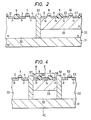
- Figure 2 is a schematic sectional view of a semi- conductor device which is an embodiment of the present invention.
- numeral 21 designates a p-type impurity layer which corresponds to the layers 3 and 4 shown in Figure 1 (hereinbelow, this figure shall be referred to), numerals 22 and 23 n-type impurity layers which correspond to the layers 5 and 6, and numeral 24 a polycrystalline silicon layer as a gate electrode which corresponds to the layer 8.
- numeral 31 indicates a heavily-doped n-type semi- conductor substrate, numeral 32 a lightly-doped n-type epitaxial layer, and numeral 33 a p-type well layer.
- the semiconductor body has a double-layer structure in which a high impurity layer 31 is overlaid with a low impurity layer 32 and that an insulator layer 30, which penetrates the low impurity layer 32 to reach the high impurity layer 31, is disposed at the boundary part between the semi-conductor body 32 and the well layer 33.
- the p-channel MOS transistor area and the n-channel MOS transistor area are perfectly isolated, by the insulator layer 30 and the high impurity layer 31.
- the semiconductor device of the present example notwithstanding that the resistivity of the heavily-doped n-type semiconductor substrate 31 is as very low as 0,1 Q. cm or less, the base current of the parasitic transistor is substantially cut off, and hence, the latch-up phenomenon being the disadvantage of the prior art is, in effect, hindered.
- the planar width of the insulator layer 30 is as small as 5 pm or less, the transistors can be disposed in proximity to each other, which is very advantageous for enhancing the density of integration.
- the groove width of the insulator layer may be shorter than the depth thereof.
- the groove width is usually 0.3-10 pm, and preferably 1-5 ⁇ m to the end of enhancing the density of integration. With a groove width smaller than 1 ⁇ m, difficulties are involved in the manufacturing process. Therefore, the groove width should of course be set scrupulously.
- the known reactive sputter etching is restored to by employing, e.g., Si 3 N 4 for a mask, whereby the deep groove whose side surface is substantially vertical is formed.
- the groove depth as predetermined is attained by adjusting the period of time of the sputtering.
- local oxidation is performed to form a thick Si0 2 film in the groove, and the Si 3 N 4 film is removed.
- an Si 3 N 4 film is deposited on the whole surface again.
- polycrystalline silicon is buried into the groove and has its exposed part oxidized so as to wholly turn into an Si0 2 film.
- the insulator layer is formed.
- an impurity opposite in the conductivity type to the substrate is introduced into the bottom of the groove to the end of preventing the appearance of . a channel.
- the Si 3 N 4 film deposited on the whole surface in the latter half of the manufacturing process may well be omitted.
- the forming method mentioned above has exemplified the case of burying the polycrystalline silicon into the groove.
- a dielectric material such as Si0 2 or Si 3 N 4 or a high polymer material can also be used unobjection- ably. These materials have attained equal effects.
- Figures 3(b) and 3(a) show a partial schematic sectional view of a semiconductor device as still another embodiment of the present invention, and a diagram of a circuit employing the semiconductor device, respectively.
- a memory e.g., static type random access memory by the use of the CMOS structure
- a flip- flop formed of nMOS transistors and high resistance loads R as shown in Figure 3(a) has heretofore been used as a memory cell thereof.
- This memory cell has as small a signal amplitude as 500 mV or less, and undergoes a malfunction due to noise from a peripheral circuit of large signal amplitude.
- insulator layers 41 and 42 which are deep enough to reach the heavily-doped impurity layer 31 are disposed to perfectly isolate a memory cell portion X and peripheral circuit portions Y.
- numerals 48, 49 and 60-65 denote n-type impurity layers, and numbers 43-47 polycrystalline silicon layers as the gates of MOS transistors.
- FIG. 4 shows a schematic sectional view of a semiconductor device which is yet another embodiment of the present invention.
- numerals 51, 52, 54 and 55 indicate p-type impurity layers
- numeral 56 indicates an n-type impurity layer.
- This structure shows a vertical bipolar transistor which employs the layer 56 as its emitter E, the layers 54 and 55 as its base B and the layer 31 as its collector C.
- the bipolar transistor is formed in such a manner that it is isolated from another element, e.g., a p-channel MOS transistor formed of the layers 3, 4 and 7 or the layers 51, 52 and 53 by deep insulator layers 57 and 58 which form the characterizing feature of the present example.
- the bipolar transistor free from the latchup phenomenon and with a small occupying area can be fabricated, and the circuit operation performance can be enhanced.
- the base length of the bipolar transistor becomes small to increase the parameter h FE , so that a higher operating performance can be attained.
- the same impurity layer as stated above may well be formed in the semiconductor surface portion of the memory cell portion in Figure 3(b).
- the present invention has been explained as to a CMOS structure in which a p-type well is formed in an n-type substrate. However, even when they are formed in opposite conductivity types, an effect similar to the foregoing is attained. Since such construction is merely different in the symbols of the conductivity types, the detailed description is omitted.
Landscapes
- Metal-Oxide And Bipolar Metal-Oxide Semiconductor Integrated Circuits (AREA)
- Semiconductor Memories (AREA)
Claims (6)
Applications Claiming Priority (2)
| Application Number | Priority Date | Filing Date | Title |
|---|---|---|---|
| JP103826/82 | 1982-06-18 | ||
| JP57103826A JPS58222558A (ja) | 1982-06-18 | 1982-06-18 | 半導体装置 |
Publications (2)
| Publication Number | Publication Date |
|---|---|
| EP0097326A1 EP0097326A1 (de) | 1984-01-04 |
| EP0097326B1 true EP0097326B1 (de) | 1987-01-28 |
Family
ID=14364213
Family Applications (1)
| Application Number | Title | Priority Date | Filing Date |
|---|---|---|---|
| EP83105880A Expired EP0097326B1 (de) | 1982-06-18 | 1983-06-15 | Halbleiteranordnung mit Wannenstruktur |
Country Status (5)
| Country | Link |
|---|---|
| EP (1) | EP0097326B1 (de) |
| JP (1) | JPS58222558A (de) |
| KR (1) | KR840009179A (de) |
| CA (1) | CA1200328A (de) |
| DE (1) | DE3369601D1 (de) |
Families Citing this family (2)
| Publication number | Priority date | Publication date | Assignee | Title |
|---|---|---|---|---|
| KR0120572B1 (ko) * | 1994-05-04 | 1997-10-20 | 김주용 | 반도체 소자 및 그 제조방법 |
| CN101032019A (zh) * | 2004-09-30 | 2007-09-05 | 皇家飞利浦电子股份有限公司 | 深沟槽电隔离中压cmos器件及其制造方法 |
Citations (7)
| Publication number | Priority date | Publication date | Assignee | Title |
|---|---|---|---|---|
| US4178605A (en) * | 1978-01-30 | 1979-12-11 | Rca Corp. | Complementary MOS inverter structure |
| EP0021776A1 (de) * | 1979-06-18 | 1981-01-07 | Fujitsu Limited | Halbleiter-Speichervorrichtung und Verfahren zu deren Herstellung |
| EP0063916A1 (de) * | 1981-04-21 | 1982-11-03 | Nippon Telegraph And Telephone Corporation | Integrierte Halbleiterschaltungen und Verfahren zu ihrer Herstellung |
| EP0074541A2 (de) * | 1981-09-10 | 1983-03-23 | Fujitsu Limited | Verfahren zur Herstellung einer Halbleiteranordnung mit dielektrischen Isolationszonen |
| EP0076942A2 (de) * | 1981-10-14 | 1983-04-20 | Kabushiki Kaisha Toshiba | Verfahren zur Herstellung von integrierten Schaltungsanordnungen mit dielektrischen Isolationszonen |
| EP0078890A2 (de) * | 1981-11-06 | 1983-05-18 | Rockwell International Corporation | Verfahren zur Herstellung einer dielektrisch isolierten CMOS-Halbleiteranordnung mit Isolationsnuten |
| EP0082256A2 (de) * | 1981-12-10 | 1983-06-29 | Kabushiki Kaisha Toshiba | Verfahren zur Herstellung von Halbleiteranordnungen mit dielektrischen Isolationszonen |
Family Cites Families (1)
| Publication number | Priority date | Publication date | Assignee | Title |
|---|---|---|---|---|
| NL160988C (nl) * | 1971-06-08 | 1979-12-17 | Philips Nv | Halfgeleiderinrichting met een halfgeleiderlichaam, be- vattende ten minste een eerste veldeffecttransistor met geisoleerde stuurelektrode en werkwijze voor de vervaar- diging van de halfgeleiderinrichting. |
-
1982
- 1982-06-18 JP JP57103826A patent/JPS58222558A/ja active Pending
-
1983
- 1983-06-15 KR KR1019830002669A patent/KR840009179A/ko not_active Withdrawn
- 1983-06-15 EP EP83105880A patent/EP0097326B1/de not_active Expired
- 1983-06-15 DE DE8383105880T patent/DE3369601D1/de not_active Expired
- 1983-06-17 CA CA000430676A patent/CA1200328A/en not_active Expired
Patent Citations (7)
| Publication number | Priority date | Publication date | Assignee | Title |
|---|---|---|---|---|
| US4178605A (en) * | 1978-01-30 | 1979-12-11 | Rca Corp. | Complementary MOS inverter structure |
| EP0021776A1 (de) * | 1979-06-18 | 1981-01-07 | Fujitsu Limited | Halbleiter-Speichervorrichtung und Verfahren zu deren Herstellung |
| EP0063916A1 (de) * | 1981-04-21 | 1982-11-03 | Nippon Telegraph And Telephone Corporation | Integrierte Halbleiterschaltungen und Verfahren zu ihrer Herstellung |
| EP0074541A2 (de) * | 1981-09-10 | 1983-03-23 | Fujitsu Limited | Verfahren zur Herstellung einer Halbleiteranordnung mit dielektrischen Isolationszonen |
| EP0076942A2 (de) * | 1981-10-14 | 1983-04-20 | Kabushiki Kaisha Toshiba | Verfahren zur Herstellung von integrierten Schaltungsanordnungen mit dielektrischen Isolationszonen |
| EP0078890A2 (de) * | 1981-11-06 | 1983-05-18 | Rockwell International Corporation | Verfahren zur Herstellung einer dielektrisch isolierten CMOS-Halbleiteranordnung mit Isolationsnuten |
| EP0082256A2 (de) * | 1981-12-10 | 1983-06-29 | Kabushiki Kaisha Toshiba | Verfahren zur Herstellung von Halbleiteranordnungen mit dielektrischen Isolationszonen |
Non-Patent Citations (1)
| Title |
|---|
| I.E.E. 1st EUROPEAN SOLID STATE CIRCUITS CONFERENCE, 1975, pages 28-29, London, G.B., C. MULDER et al.: "High-speed I2L" * |
Also Published As
| Publication number | Publication date |
|---|---|
| DE3369601D1 (en) | 1987-03-05 |
| KR840009179A (ko) | 1984-12-24 |
| EP0097326A1 (de) | 1984-01-04 |
| JPS58222558A (ja) | 1983-12-24 |
| CA1200328A (en) | 1986-02-04 |
Similar Documents
| Publication | Publication Date | Title |
|---|---|---|
| JP2950558B2 (ja) | 半導体装置 | |
| JP2851753B2 (ja) | 半導体装置およびその製造方法 | |
| JP2703970B2 (ja) | Mos型半導体装置 | |
| US4826780A (en) | Method of making bipolar transistors | |
| US6020614A (en) | Method of reducing substrate noise coupling in mixed signal integrated circuits | |
| JPH0271556A (ja) | 半導体装置 | |
| KR100275962B1 (ko) | 반도체장치 및 그의 제조방법_ | |
| US8445970B2 (en) | Bipolar device compatible with CMOS process technology | |
| US4484211A (en) | Oxide walled emitter | |
| JPH05129429A (ja) | 半導体装置およびその製造方法 | |
| US5191401A (en) | MOS transistor with high breakdown voltage | |
| EP0178991B1 (de) | "Latch-up"-freie komplementäre Halbleiteranordnung mit hoher Schaltgeschwindigkeit | |
| US3639813A (en) | Complementary enhancement and depletion mosfets with common gate and channel region, the depletion mosfet also being a jfet | |
| GB1563863A (en) | Igfet inverters and methods of fabrication thereof | |
| US3770519A (en) | Isolation diffusion method for making reduced beta transistor or diodes | |
| JP3400891B2 (ja) | 半導体記憶装置およびその製造方法 | |
| KR860000159B1 (ko) | 반도체 메모리 | |
| EP0399454B1 (de) | Monolithische Halbleiteranordnung mit CCD-, bipolaren und MOS-Strukturen | |
| US5057894A (en) | Semiconductor integrated circuit device | |
| EP0097326B1 (de) | Halbleiteranordnung mit Wannenstruktur | |
| US5122855A (en) | Semiconductor device with latch-up prevention structure | |
| KR200158788Y1 (ko) | 반도체장치 | |
| KR100356827B1 (ko) | 반도체장치의 웰 및 그 형성방법 | |
| JPS61156830A (ja) | 半導体装置およびその製造方法 | |
| JP2680846B2 (ja) | 半導体記憶装置 |
Legal Events
| Date | Code | Title | Description |
|---|---|---|---|
| PUAI | Public reference made under article 153(3) epc to a published international application that has entered the european phase |
Free format text: ORIGINAL CODE: 0009012 |
|
| AK | Designated contracting states |
Designated state(s): DE FR GB NL |
|
| 17P | Request for examination filed |
Effective date: 19840131 |
|
| GRAA | (expected) grant |
Free format text: ORIGINAL CODE: 0009210 |
|
| AK | Designated contracting states |
Kind code of ref document: B1 Designated state(s): DE FR GB NL |
|
| REF | Corresponds to: |
Ref document number: 3369601 Country of ref document: DE Date of ref document: 19870305 |
|
| ET | Fr: translation filed | ||
| PG25 | Lapsed in a contracting state [announced via postgrant information from national office to epo] |
Ref country code: GB Effective date: 19870615 |
|
| PLBI | Opposition filed |
Free format text: ORIGINAL CODE: 0009260 |
|
| 26 | Opposition filed |
Opponent name: TELEFUNKEN ELECTRONIC GMBH Effective date: 19871027 |
|
| PG25 | Lapsed in a contracting state [announced via postgrant information from national office to epo] |
Ref country code: NL Effective date: 19880101 |
|
| NLR1 | Nl: opposition has been filed with the epo |
Opponent name: TELEFUNKEN ELECTRONIC GMBH |
|
| NLV4 | Nl: lapsed or anulled due to non-payment of the annual fee | ||
| PG25 | Lapsed in a contracting state [announced via postgrant information from national office to epo] |
Ref country code: DE Effective date: 19880301 |
|
| GBPC | Gb: european patent ceased through non-payment of renewal fee | ||
| PG25 | Lapsed in a contracting state [announced via postgrant information from national office to epo] |
Ref country code: FR Free format text: LAPSE BECAUSE OF NON-PAYMENT OF DUE FEES Effective date: 19890228 |
|
| REG | Reference to a national code |
Ref country code: FR Ref legal event code: ST |
|
| RDAG | Patent revoked |
Free format text: ORIGINAL CODE: 0009271 |
|
| STAA | Information on the status of an ep patent application or granted ep patent |
Free format text: STATUS: PATENT REVOKED |
|
| 27W | Patent revoked |
Effective date: 19890318 |
|
| GBPR | Gb: patent revoked under art. 102 of the ep convention designating the uk as contracting state |