EP0097524B1 - Dispositif de mémoire à bulles magnétiques - Google Patents
Dispositif de mémoire à bulles magnétiques Download PDFInfo
- Publication number
- EP0097524B1 EP0097524B1 EP83303563A EP83303563A EP0097524B1 EP 0097524 B1 EP0097524 B1 EP 0097524B1 EP 83303563 A EP83303563 A EP 83303563A EP 83303563 A EP83303563 A EP 83303563A EP 0097524 B1 EP0097524 B1 EP 0097524B1
- Authority
- EP
- European Patent Office
- Prior art keywords
- bubble
- pattern
- gate
- minor
- mla
- Prior art date
- Legal status (The legal status is an assumption and is not a legal conclusion. Google has not performed a legal analysis and makes no representation as to the accuracy of the status listed.)
- Expired
Links
Images





Classifications
-
- G—PHYSICS
- G11—INFORMATION STORAGE
- G11C—STATIC STORES
- G11C19/00—Digital stores in which the information is moved stepwise, e.g. shift registers
- G11C19/02—Digital stores in which the information is moved stepwise, e.g. shift registers using magnetic elements
- G11C19/08—Digital stores in which the information is moved stepwise, e.g. shift registers using magnetic elements using thin films in plane structure
- G11C19/0875—Organisation of a plurality of magnetic shift registers
- G11C19/0883—Means for switching magnetic domains from one path into another path, i.e. transfer switches, swap gates or decoders
- G11C19/0891—Means for switching magnetic domains from one path into another path, i.e. transfer switches, swap gates or decoders using hybrid structure, e.g. ion doped layers
Definitions
- the present invention relates to a magnetic bubble memory device which is used as a memory device for an electronic computer or for a terminal device of the computer. More particularly, the present invention relates to the constitution of a gate which operably associates a major line with a minor loop in a major-minor loop-organized magnetic bubble memory device.
- magnétique bubble memory device which comprises a thin layer of magnetic material in which magnetic bubbles can propagate along propagation paths in response to a magnetic drive field rotating or reorienting cyclically in the plane of the magnetic layer.
- One of the most common arrangements of the propagation paths for magnetic bubble memory devices is a major-minor loop organization. This organization includes a plurality of minor loops for the storage of bubble information and one or two major lines, or loops, for the propagation of bubble information between a bubble generator and the minor loops and between the minor loops and a bubble detector.
- the major line or lines and the minor loops are operably associated with each other through gates which perform various functions, such as the transfer, replication, or swapping of bubbles, whereby the writing in of and the reading out of bubble information between the major line or lines and the minor loops are performed.
- propagation paths There are two well-known kinds of propagation paths, one being defined by elements or patterns of magnetically soft material such as permalloy and commonly referred to as a "permalloy propagation path" and the other being defined by an ion-implanted pattern and commonly referred to as an "ion-implanted propagation path". It is well known in the art that the minimum geometric size required for forming an ion-implanted propagation path is larger than that required for forming a permalloy propagation path, and, accordingly, an ion-implanted propagation path is a very promising means for providing a high-density storage magnetic bubble memory device in which the bit period is 4 ⁇ m or less and the memory capacity is 4 Mbit or more.
- US-A-4040019 describes a magnetic bubble memory device comprising: a magnetic layer in which magnetic bubbles can be moved; at least one major line and a plurality of minor loops for the storage of information, along which bubbles propagate in the magnetic layer in response to a magnetic drive field rotating in the plane of the magnetic layer, the major line having gate portions and propagation elements of permalloy formed on the magnetic layer, the minor loops being defined by an ion implanted pattern in the magnetic layer and having gate portions provided with cusps; and, a plurality of gates operably associating the major line with the minor loops and comprising conductor patterns extending between the gate portions of the major line and the gate portions of the minor loops, the pickax pattern having its head portion disposed closer to the cusp in the gate portion of its associated minor loops than its tail portion.
- such a magnetic bubble memory device is characterised in that the gate portion comprises pickax patterns of permalloy, in that the minor loops are provided with cusps at the gate portion in that the minor loop is of the folded type with said cusp provided at a gap formed between two track portions of the minor loop, in that each of the conductor patterns is formed into a meandering configuration having a first U-shaped pattern extending between the head portion of the pickax pattern and the gate portion cusp of the minor loop and inclined with respect to the easy axis of strip-out, the inclination being in the direction of rotation of the drive field, and a second U-shaped pattern extending in a direction opposite to that of the first pattern and aligned with the tail portion of the pickax pattern, the second U-shaped pattern being colinear with the easy axis of strip out or being inclined with respect to it in the direction of rotation of the drive field.
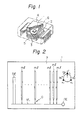
- a magnetic bubble memory device comprises: a magnetic bubble memory chip 1; two coils 2 and 3 disposed perpendicular to each other and adapted to generate a magnetic field rotating or reorienting cyclically in the plane of the chip 1 so as to drive magnetic bubbles in the chip 1; permanent magnets 4 and 5 adapted to generate a bias magnetic field so as to stably maintain the magnetic bubbles; and a shield case 6 (indicated by the phantom line).
- the memory chip 1 comprises a substrate of gadolinium-gallium-garnet (not illustrated) on which a thin layer of magnetic material 7, a bubble generator GE, a bubble detector DE, a major line ML, a plurality of minor loops ml, and replicate/swap gates G are formed.
- the symbol K 1 designates the easy axes of stripe-out in the magnetic layer 7.
- the magnetic bubbles can be propagated in the magnetic layer 7 along the major line ML and the minor loops ml in response to rotation of reorientation of the in-plane drive field H D .
- the minor loops ml constitute a storage section for storing bubble information.
- the major line ML constitutes a means for the propagation of bubble information between the generator GE and the minor loops ml and between the minor loops ml and the detector DE.
- the major line ML is operably associated with the minor loops ml through the replicate/swap gates G, and thereby the writing or bubble information from the major line ML into the minor loops ml and reading out of bubble information from the minor loops ml into the major line ML are performed.
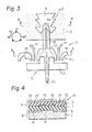
- the magnetic layer 7 is provided with an ion-implanted pattern, which is formed therein by a well-known ion-implantation technique and which includes an ion-implanted region 8 and a plurality of non-implanted regions 9 surrounded by the ion-implanted region 8.
- the minor loops ml are defined by the respective peripheries of the non-implanted regions 9.
- Each of the minor loops ml has a straight configuration extending parallel to one of the easy axes K 1 of stripe-out in the magnetic layer 7 and is provided in the gate portion (the lower portion of the minor loop) with a cusp 9a associated with the gate G.
- two layers of spacers 11 and 12 of insulating material are formed on the magnetic layer 7.
- two layers of spacers 11 and 12 of insulating material are formed in the region of the spacer 12, which corresponds to a non-implanted region 10 in the magnetic layer 7, there are formed a plurality of permalloy patterns or elements, including pickax patterns 13, bar patterns 14 and 14', and half-disk patterns 15, which define the major line ML.
- the pickax patterns 13 are disposed adjacent to the gate portions of the minor loops ml and constitute the gate portions of the major line ML associated with the gates G.
- Each of the pickax patterns 13 has a center line CL which is parallel to the easy axis K, of stripe-out to which the minor loops ml extend in parallel, and which is aligned with the cusp 9a in the gate portion of the minor loop ml.
- a conductor CD is formed between the spacers 11 and 12 and has a plurality of U-shaped patterns or hairpin loops 16.
- Each of the hairpin loops 16 extends along the center line CL of the pickax pattern 13 between the head portion of the pickax pattern 13 and the gate portion cusp 9a of the minor loop ml, and thereby the replicate gate G is constructed.
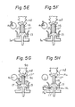
- Figs. 5A through 5H and Fig. 6 Referring first to Fig. 5A, when the drive field He is at phase 8 0 , a bubble 17 propagating along the minor loop ml in the direction of the arrow Pm is trapped in the gate portion cusp 9a.
- a bubble-stretch current I ST is applied to the conductor CD from phase ⁇ 1 to phase 8 2 of the drive field H o so that the bubble 17 is stretched along the inner edges of the conductor hairpin loop 16 between the cusp 9a of the minor loop ml and the head portion of the pickax pattern 13 of the major line ML.
- Fig. 5A when the drive field He is at phase 8 0 , a bubble 17 propagating along the minor loop ml in the direction of the arrow Pm is trapped in the gate portion cusp 9a.
- Fig. 5B a bubble-stretch current I ST is applied to the conductor CD from phase ⁇ 1 to phase 8 2 of the drive field H o so
- the stretch current I ST is turned off at phase 8 2 of the drive field He so that the stretched bubble 17 is shrunk, is attracted to the head portion of the pickax pattern 13, and is stretched along the top edge of the pickax pattern 13 across the hairpin loop 16.
- a bubble-cut current l c having a polarity opposite to that of the stretch current I ST is applied to the conductor CD so that the bubble 17 is divided into two bubbles 17' and 17".
- the cut current I c is applied until the drive field H o rotates to phase 6 3 .
- a bubble-return current I R having the same polarity as but having a magnitude smaller than the cut current l c , is applied to the conductor CD from phase 8 3 to phase 8 4 of the drive field H D .
- the two bubbles 17' and 17" are stretched along the respective outer edges of the hairpin loop 16 between the pickax pattern 13 and the minor loop ml and remain stretched.
- the return current I R is turned off at phase ⁇ 4 .
- the left side 9b and the right side 9c of the cusp 9a become magnetically repulsive and attractive, respectively, to the bubbles while the left shoulder 13a and the right shoulder 13b of the head portion of the pickax pattern 13 become magnetically attractive and repulsive, respectively, to the bubbles. Accordingly, the bubbles 17' and 17" are attracted to the pickax pattern 13 and the minor loop ml, respectively.
- the drive field He further rotates, as illustrated in Fig. 5H
- the bubble 17' on the major line ML propagates in the direction of the arrow P m
- the bubble 17" on the minor loop ml propagates in the direction of the arrow P m , whereby the replicate operation is completed. Therefore, the non-destructive readout of bubble information stored in the minor loops ml into the major ML is performed.
- Figs. 7A through 7D and Fig. 8 Referring first to Fig. 7A, when the drive field H D is at phase ⁇ 0 , a bubble 17 on the minor loop ml and a bubble 18 on the major line ML propagate to the illustrated positions in the direction of the arrows P m and P M , respectively.
- a bubble-stretch current I ST is applied to the conductor CD from phase 8 1 to phase 8 2 of the drive field H D so that the bubbles 17 and 18 are stretched along the outer edges of the conductor hairpin loop 16 between the gate portion of the minor loop ml and the head portion of the pickax pattern 13 and remain stretched.
- the stretch current I ST is turned off at phase 8 2 of the drive field H D so that the bubbles 17 and 18 are shrunk and are attracted to the pickax pattern 13 and the minor loop ml, respectively, in the manner previously described with reference to Fig. 5G.
- the drive field H D further rotates, as illustrated in Fig. 7D, the bubble 17 on the major line ML propagates in the direction of the arrow P m while the bubble 18 on the minor loop ml propagates in the direction of the arrow P m , and thereby the swap operation is completed. Therefore, the new bubble information on the major line ML is substituted for the old bubble information stored in the minor loops ml, i.e., the rewriting of information is performed.
- replicate/swap gates G can act as transfer-in gates for the transfer of bubble information from the major line to the minor loops or as transfer-out gates for the transfer'of bubble information from the minor loop to the major line in the same manner as the above-described swap operation.
- the minor loops for the storage of the bubble information are defined by an ion-implanted pattern. Accordingly, it is possible to provide high-density storage as previously described.
- the gate portions of the major line are defined by permalloy patterns, and, accordingly, it is possible to provide gates superior in operating margins. It should be noted that the major line in the above-described embodiment is defined entirely by permalloy patterns. However, the gate portions of the major line need be defined only by permalloy patterns, and the portions other than the gate portions may be defined by ion-implanted patterns.
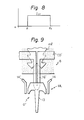
- a gate G' is a modification of the gate G illustrated in Fig. 3, in which the same parts are designated by the same reference numerals and symbols as in Fig. 3.
- the gate G' is basically the same in constitution, operation, and function as the gate G, there being only one difference in that a conductor CD' is turned by 180° as compared to the conductor CD.
- Fig. 10 there is illustrated a modification of the memory chip constitution illustrated in Fig. 2.
- the major line ML and the gates G are the same as those illustrated in Fig. 3, but the minor loops ml' are different from those illustrated in Fig. 3.
- Each minor loop ml' has a folded configuration which is formed by interconnecting three straight minor loops, such as the minor loops ml illustrated in Figs. 2 and 3, at the ends thereof adjacent to the major line.
- This constitution is advantageous in that the gates G can be arranged at longer intervals.
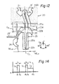
- a memory chip 1A is provided with a bubble generation GE, a bubble detector DE, two major lines ML 1 and ML 2 , a plurality of minor loops miA, a swap gate G 1 , and a replicate gate G 2 .
- the first major line ML 1 is adapted for the propagation of bubble information from the generator GE to the minor loops miA, and the swap gate G 1 functions to write bubble information from the major line ML 1 into the minor loops mIA.
- the second major line ML 2 is adapted for the propagation of bubble information from the minor loops mIA to the detector DE, and the replicate gate G 2 functions to read bubble information out of the minor loops. mlA into the major line ML 2 .
- the memory chip 1A has basically the same sectional constitution as that described with reference to Fig. 4.
- each of the minor loops mIA is defined in the magnetic layer by the outer edges of a pair of non-implanted regions 21 and 21' which are opposed to each other with a small gap therebetween and which are surrounded by an ion-implanted region 20.
- Each of the minor loops mlA is folded into a U-shaped configuration and is provided with a cusp 21a in the gate portion associated with the gate G 2 .
- Fig. 11 the constitution of the major line ML 1 and the swap gate G 1 for writing in bubble information is the same as that illustrated in Fig. 3 or Fig. 9 except that it is turned by 180°.
- the operation of the swap gate G 1 is the same as that previously described with reference to Figs. 7A through 7D and Fig. 8.
- the major line ML 2 for the reading out of bubble information is defined, like the major lines ML and ML 1 , by permalloy patterns.
- the major line ML 2 has auxiliary paths MLa.
- each of the auxiliary paths MLa is defined by a plurality of permalloy patterns, including a pickax pattern 22, bar patterns 23 and 23', and half-disk patterns 24.
- the pickax patterns 22 of the auxiliary paths MLa are disposed adjacent to the gate portion cusps 21a of the minor loops mIA and constitute the gate portions of the major line ML 2 .
- Each of the pickax patterns 22 has a center line CL which is parallel to one of the easy axes K, of strip-out in the magnetic layer and is aligned with the cusp 21 a.
- a conductor CDA is formed between the minor loops mIA and the major line ML 2 and has a plurality of meandering patterns 25.
- Each of the meandering patterns 25 has two U-shaped patterns or hairpin loops 25a and 25b which extend in opposite directions.
- the first hairpin loop 25a extends between the right shoulder 22b of the head portion of the pickax pattern 22 and the gate portion cusp 21 a of the minor loop mIA
- the second hairpin loop 25b extends between the middle 22a of the head portion and the tail end 22c of the pickax pattern 22, thereby forming the replicate gate G 2 .
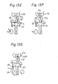
- Fig. 13A when the drive field H D is at phase ⁇ 1 , a bubble 26 propagating along the minor loop mlA in the direction of the arrow P m is trapped in the gate portion cusp 21 a. From phase 8 1 to phase ⁇ 2 of the drive field H D , a bubble-stretch current I ST is applied to the conductor CDA so that the bubble 26 is stretched along the inner edges of the first hairpin loop 25a between the cusp 21 a of the minor loop mIA and the right shoulder 22b of the pickax pattern 22. Referring to Fig.
- the stretch current I ST is turned off at phase 8 2 so that the stretched bubble 26 is shrunk, is attracted to the pickax pattern 22, and is stretched along the top edge of the pickax pattern 22 across the second hairpin loop 25b.
- a bubble-cut current I c which has the same polarity as the stretch current I ST , is applied to the conductor CDA from phase ⁇ 3 to phase ⁇ 4 of the drive field H D , with the result that the bubble 26 is divided into two bubbles 26' and 26".
- a bubble-return current I R which has the same polarity as but has a smaller magnitude than the cut current I c , is applied to the conductor CDA from phase 8 4 to phase 8 5 of the drive field H D , with the result that the bubble 26' remains trapped on the pickax pattern 22 but the bubble 26" is again stretched along the inner edges of the first hairpin loop 25a between the pickax pattern 22 and the gate portion cusp 21a of the minor loop mIA.
- the return current I R is turned off at phase ⁇ 5 of the drive field H D .
- the right shoulder 22b of the pickax pattern 22 and the cusp 21a a of the minor loop mIA becomes magnetically repulsive and attractive, respectively, to the bubbles and, accordingly, the bubble 26" is shrunk and is attracted to the minor loop mIA.
- the drive field H D further rotates, as illustrated in Fig. 13G, the bubble 26' on the pickax pattern 22 propagates in the direction of the arrow P M while the bubble 26" on the minor loop mlA propagates in the direction of the arrow P m , and thereby the replicate operation is completed.
- replicate gates G 2 can act as transfer-out gates for the transfer of bubble information from the minor loops to the major line, if the stretch current I ST only is applied, but the cut current I c and the return current I R are not applied, to the conductor CDA.
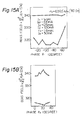
- Figures 15A and 15B illustrate the operating characteristics in the replicate gate G 2 .
- Figure 15A illustrates phase margins in relation to phase ⁇ 1 , at which the pulse of the stretch current I ST rises
- Fig. 15B illustrates phase margins in relation to phase 8 3 , at which the pulse of the cut current I c rises, provided that the bubble diameter is 1 pm
- the drive field H D is 6365 A/m (80 Oe)
- the stretch current I ST is 100 mA
- the cut current I c is 100 mA
- the return current I R is 50 mA
- the current pulse durations t 1 , t 2 , and t 3 are 1 ⁇ sec, 0.5 ⁇ sec, and 1.6 ⁇ sec, respectively.
- the replicate gate G 2 described above is advantageous as compared with the gate G illustrated in Fig. 3. That is, in the gate G, it is required that the stretch current I ST have a polarity opposite to those of the cut current I c and the return current I R in the replicate operation thereof, as was previously described with reference to Figs. 5A through 5H and Fig. 6, and, accordingly, the gate driving circuit is complicated. In the gate G 2 , contrary to the above, the stretch current I ST , the cut current I c , and the return current I R have the same polarity, and therefore the gate driving circuit can be simplified.
- the gate G 2 has a disadvantage in that, as will be understood from Figs. 13C and 13D, the interval between the phase at which the bubble starts to stretch and the phase which is appropriate for cutting the bubble is small. Namely, the time margin for bubble stretching is small.
- FIG 16 illustrates an improved gate G 2 ' the aim of which is to eliminate the above-described disadvantage.
- the gate G 2 ' is basically the same in constitution as the gate G 2 .
- the gate G 2 ' is characterized in that a tail portion 27 of a pickax pattern 22' and a second hairpin loop 25b' of a meandering pattern of a conductor CDA' are inclined at an angle a with respect to the center line CL of the pickax pattern 22' in the direction of rotation of the drive field H D .
- the phase appropriate for cutting the bubble stretched on the pickax pattern 22' is later than that for the gate G 2 , and, accordingly, the time margin for bubble stretching on the pickax pattern 22' is greatly increased.
Landscapes
- Thin Magnetic Films (AREA)
- Hall/Mr Elements (AREA)
- Mram Or Spin Memory Techniques (AREA)
Claims (3)
Applications Claiming Priority (4)
| Application Number | Priority Date | Filing Date | Title |
|---|---|---|---|
| JP57106666A JPS58224493A (ja) | 1982-06-23 | 1982-06-23 | 磁気バルブメモリデバイス |
| JP106666/82 | 1982-06-23 | ||
| JP34632/83 | 1983-03-04 | ||
| JP58034632A JPS59162683A (ja) | 1983-03-04 | 1983-03-04 | 磁気バブルメモリデバイス |
Publications (3)
| Publication Number | Publication Date |
|---|---|
| EP0097524A2 EP0097524A2 (fr) | 1984-01-04 |
| EP0097524A3 EP0097524A3 (en) | 1986-10-15 |
| EP0097524B1 true EP0097524B1 (fr) | 1989-08-30 |
Family
ID=26373459
Family Applications (1)
| Application Number | Title | Priority Date | Filing Date |
|---|---|---|---|
| EP83303563A Expired EP0097524B1 (fr) | 1982-06-23 | 1983-06-21 | Dispositif de mémoire à bulles magnétiques |
Country Status (4)
| Country | Link |
|---|---|
| US (1) | US4561069A (fr) |
| EP (1) | EP0097524B1 (fr) |
| CA (1) | CA1197924A (fr) |
| DE (1) | DE3380503D1 (fr) |
Families Citing this family (1)
| Publication number | Priority date | Publication date | Assignee | Title |
|---|---|---|---|---|
| US4744052A (en) * | 1985-07-03 | 1988-05-10 | Hitachi, Ltd. | Hybrid magnetic bubble memory device |
Family Cites Families (4)
| Publication number | Priority date | Publication date | Assignee | Title |
|---|---|---|---|---|
| US4040019A (en) * | 1974-08-23 | 1977-08-02 | Texas Instruments Incorporated | Ion implanted magnetic bubble memory device having major and minor rows |
| GB1527005A (en) * | 1975-12-31 | 1978-10-04 | Ibm | Method and apparatus for magnetic bubble storage |
| US4415988A (en) * | 1980-07-15 | 1983-11-15 | Fujitsu Limited | Magnetic bubble memory device |
| US4360904A (en) * | 1980-10-27 | 1982-11-23 | Rockwell International Corporation | Segmented stretcher detector for magnetic bubble domain devices |
-
1983
- 1983-06-16 CA CA000430571A patent/CA1197924A/fr not_active Expired
- 1983-06-20 US US06/505,978 patent/US4561069A/en not_active Expired - Fee Related
- 1983-06-21 EP EP83303563A patent/EP0097524B1/fr not_active Expired
- 1983-06-21 DE DE8383303563T patent/DE3380503D1/de not_active Expired
Non-Patent Citations (1)
| Title |
|---|
| A.H. Eschenfelder "Magnetic Bubble Technology", Second Edition, Springer Verlag 1981, p. 109-113 and p. 128-137, p. 12-13 * |
Also Published As
| Publication number | Publication date |
|---|---|
| CA1197924A (fr) | 1985-12-10 |
| US4561069A (en) | 1985-12-24 |
| DE3380503D1 (en) | 1989-10-05 |
| EP0097524A2 (fr) | 1984-01-04 |
| EP0097524A3 (en) | 1986-10-15 |
Similar Documents
| Publication | Publication Date | Title |
|---|---|---|
| US3909810A (en) | Bubble memory minor loop redundancy scheme | |
| US4079461A (en) | Gap tolerant bubble domain propagation circuits | |
| US4056812A (en) | Fault tolerant magnetic bubble memory | |
| US4561069A (en) | Magnetic bubble memory device gates | |
| US3916395A (en) | Cylindrical magnetic domain storage device having wave-like magnetic wall | |
| US4414648A (en) | Magnetic bubble domain swap gate circuit | |
| EP0081215B1 (fr) | Mémoire à bulles magnétiques | |
| CA1165874A (fr) | Memoire a bulles magnetiques | |
| US4164026A (en) | Contiguous element field access bubble lattice file | |
| US4276614A (en) | Ion-implanted magnetic bubble memory with merge port | |
| US4316263A (en) | Transfer and replication arrangement for magnetic bubble memory devices | |
| US4486858A (en) | Magnetic-bubble memory device | |
| US3713119A (en) | Domain propagation arrangement | |
| US3736577A (en) | Domain transfer between adjacent magnetic chips | |
| US4070659A (en) | Magnetic bubble domain memory chip with major/minor bubble path configuration | |
| US4156937A (en) | Noncirculating register for bubble memory systems | |
| US4744052A (en) | Hybrid magnetic bubble memory device | |
| US4388700A (en) | Nucleation bubble generator for bubble domain devices | |
| JPS5927031B2 (ja) | 磁気バブル記憶装置 | |
| JP2616906B2 (ja) | ブロッホラインメモリ | |
| JPS599109B2 (ja) | 磁気バルブ記憶装置 | |
| EP0044961A1 (fr) | Commutateur sans conducteur pour le transfert de bulles | |
| JPS6160503B2 (fr) | ||
| JPH0456393B2 (fr) | ||
| JPS6118276B2 (fr) |
Legal Events
| Date | Code | Title | Description |
|---|---|---|---|
| PUAI | Public reference made under article 153(3) epc to a published international application that has entered the european phase |
Free format text: ORIGINAL CODE: 0009012 |
|
| AK | Designated contracting states |
Designated state(s): DE FR GB |
|
| PUAL | Search report despatched |
Free format text: ORIGINAL CODE: 0009013 |
|
| AK | Designated contracting states |
Kind code of ref document: A3 Designated state(s): DE FR GB |
|
| 17P | Request for examination filed |
Effective date: 19870313 |
|
| 17Q | First examination report despatched |
Effective date: 19871125 |
|
| GRAA | (expected) grant |
Free format text: ORIGINAL CODE: 0009210 |
|
| AK | Designated contracting states |
Kind code of ref document: B1 Designated state(s): DE FR GB |
|
| REF | Corresponds to: |
Ref document number: 3380503 Country of ref document: DE Date of ref document: 19891005 |
|
| PGFP | Annual fee paid to national office [announced via postgrant information from national office to epo] |
Ref country code: FR Payment date: 19891127 Year of fee payment: 8 |
|
| ET | Fr: translation filed | ||
| PGFP | Annual fee paid to national office [announced via postgrant information from national office to epo] |
Ref country code: GB Payment date: 19900608 Year of fee payment: 8 |
|
| PLBE | No opposition filed within time limit |
Free format text: ORIGINAL CODE: 0009261 |
|
| STAA | Information on the status of an ep patent application or granted ep patent |
Free format text: STATUS: NO OPPOSITION FILED WITHIN TIME LIMIT |
|
| PGFP | Annual fee paid to national office [announced via postgrant information from national office to epo] |
Ref country code: DE Payment date: 19900821 Year of fee payment: 8 |
|
| 26N | No opposition filed | ||
| PG25 | Lapsed in a contracting state [announced via postgrant information from national office to epo] |
Ref country code: GB Effective date: 19910621 |
|
| GBPC | Gb: european patent ceased through non-payment of renewal fee | ||
| PG25 | Lapsed in a contracting state [announced via postgrant information from national office to epo] |
Ref country code: FR Effective date: 19920228 |
|
| PG25 | Lapsed in a contracting state [announced via postgrant information from national office to epo] |
Ref country code: DE Effective date: 19920401 |