EP0097574B1 - Integrierte binäre Addierzelle mit drei Eingängen und schnellem Summendurchlauf - Google Patents
Integrierte binäre Addierzelle mit drei Eingängen und schnellem Summendurchlauf Download PDFInfo
- Publication number
- EP0097574B1 EP0097574B1 EP83401185A EP83401185A EP0097574B1 EP 0097574 B1 EP0097574 B1 EP 0097574B1 EP 83401185 A EP83401185 A EP 83401185A EP 83401185 A EP83401185 A EP 83401185A EP 0097574 B1 EP0097574 B1 EP 0097574B1
- Authority
- EP
- European Patent Office
- Prior art keywords
- gate
- input
- output
- transistor
- variable
- Prior art date
- Legal status (The legal status is an assumption and is not a legal conclusion. Google has not performed a legal analysis and makes no representation as to the accuracy of the status listed.)
- Expired
Links
Images
Classifications
-
- G—PHYSICS
- G06—COMPUTING OR CALCULATING; COUNTING
- G06F—ELECTRIC DIGITAL DATA PROCESSING
- G06F7/00—Methods or arrangements for processing data by operating upon the order or content of the data handled
- G06F7/38—Methods or arrangements for performing computations using exclusively denominational number representation, e.g. using binary, ternary, decimal representation
- G06F7/48—Methods or arrangements for performing computations using exclusively denominational number representation, e.g. using binary, ternary, decimal representation using non-contact-making devices, e.g. tube, solid state device; using unspecified devices
- G06F7/50—Adding; Subtracting
- G06F7/501—Half or full adders, i.e. basic adder cells for one denomination
Definitions
- the invention relates to a binary addition cell with three inputs for fast propagation of the sum, produced in an integrated circuit.
- This type of multiplier is much slower than the so-called parallel multipliers where the propagation of the information is carried out asynchronously, but it makes it possible to decrease by approximately a power of ten the surface of silicon necessary for its realization compared to the surface of silicon necessary for the realization of a multiplier of parallel type of the same power.
- This circuit for producing the reservoir provides on its output the retention variable R.
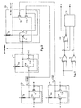
- FIG. 1 represents a diagram of the addition cell with three inputs A, B and C and two outputs S and R according to the present invention.
- This cell comprises three exclusive OR gates supplemented P1, P2 and P3 with two inputs and a PO circuit for developing the reserve R from the output signals supplied by the complemented exclusive OR gates.
- the second complemented exclusive OR gate P2 receives on its first input this first intermediate variable F i and on its second input the third binary input variable C. It outputs the binary sum variable S which constitutes the first output variable of the addition cell.
- FIG. 2 represents an addition cell, according to the present invention, produced in an MOS integrated circuit. It has fourteen elements including ten transistors and four resistant elements.
- the circuit PO for developing the reservoir R comprises four transistors T1, T2, T3 and T4 and a resistant element T5.
- the drain and the source of each of the tran sistors will be confused under the common name of “terminal”, the indeterminacy being able to be lifted in an obvious way by the person skilled in the art from the direction of the current imposed by the source used. Only the grid will therefore be named.
- the second terminal of the resistive element T5 is connected to the power supply.
- the second terminal of transistor T1 is connected to the gate of transistor T4.
- the second terminal of transistor T2 is connected to the gate of transistor T3.
- the second terminal of the dipole constituted by the transistors T3 and T4 is connected to the gate of the transistor T1, itself connected to the gate of the transistor T2. This point common to the gates of these transistors T1 and T2 constitutes the first input of this circuit for developing the reservoir R and receives from the second gate P2 the sum variable S.
- the sum S and the intermediate variables F 1 and F 3 are produced using three identical cells, with MOS transistors, of known type, making it possible to produce, using only two MOS transistors and one resistant element, an exclusive OR door completed.
- the resistive element T8 has its second terminal connected to the power supply.
- the first transistor T6 has its second terminal connected to the gate of the second transistor T7 and receives, as well as this gate, the second input variable B.
- the second transistor T7 has its second terminal connected to the gate of the first transistor T6 and receives , as well as this grid, the first input variable A.
- the second gate P2 comprises two transistors T9 and T10 and a resistant element T11. These three elements have a common terminal like the elements T6, T7 and T8 of the first terminal.
- This second gate P2 is identical to the first, the transistor T9 replacing the transistor T6, the transistor T10 replacing the transistor T7 and the resistive element T11 replacing the resistive element T8.
- the third gate P3 is identical to the first two gates P1 and P2 and comprises as transistor T12 the first transistor, as transistor T13 as second transistor and as resistance element the resistance element T14.
- the gate of the first transistor receives the first input variable A of the addition cell and the gate of the second transistor T13 receives its second input variable C which constitutes the third input variable of the cell.
Landscapes
- Physics & Mathematics (AREA)
- General Physics & Mathematics (AREA)
- Engineering & Computer Science (AREA)
- Computational Mathematics (AREA)
- Mathematical Analysis (AREA)
- Pure & Applied Mathematics (AREA)
- Theoretical Computer Science (AREA)
- Computing Systems (AREA)
- Mathematical Optimization (AREA)
- General Engineering & Computer Science (AREA)
- Logic Circuits (AREA)
- Design And Manufacture Of Integrated Circuits (AREA)
Claims (3)
Applications Claiming Priority (2)
| Application Number | Priority Date | Filing Date | Title |
|---|---|---|---|
| FR8210025A FR2528596A1 (fr) | 1982-06-09 | 1982-06-09 | Cellule d'addition binaire a trois entrees a propagation rapide de la somme, realisee en circuit integre |
| FR8210025 | 1982-06-09 |
Publications (2)
| Publication Number | Publication Date |
|---|---|
| EP0097574A1 EP0097574A1 (de) | 1984-01-04 |
| EP0097574B1 true EP0097574B1 (de) | 1987-09-16 |
Family
ID=9274797
Family Applications (1)
| Application Number | Title | Priority Date | Filing Date |
|---|---|---|---|
| EP83401185A Expired EP0097574B1 (de) | 1982-06-09 | 1983-06-09 | Integrierte binäre Addierzelle mit drei Eingängen und schnellem Summendurchlauf |
Country Status (6)
| Country | Link |
|---|---|
| US (1) | US4547863A (de) |
| EP (1) | EP0097574B1 (de) |
| JP (1) | JPS5962952A (de) |
| BE (1) | BE896999R (de) |
| DE (1) | DE3373727D1 (de) |
| FR (1) | FR2528596A1 (de) |
Families Citing this family (11)
| Publication number | Priority date | Publication date | Assignee | Title |
|---|---|---|---|---|
| JPS59139447A (ja) * | 1983-01-28 | 1984-08-10 | Matsushita Electric Ind Co Ltd | 全加算器 |
| EP0122946B1 (de) * | 1983-04-15 | 1987-09-09 | Deutsche ITT Industries GmbH | CMOS-Volladdierstufe |
| JPS60247733A (ja) * | 1984-05-24 | 1985-12-07 | Toshiba Corp | 論理演算回路 |
| JPS60247734A (ja) * | 1984-05-24 | 1985-12-07 | Toshiba Corp | 論理演算回路 |
| US4718034A (en) * | 1984-11-08 | 1988-01-05 | Data General Corporation | Carry-save propagate adder |
| US4709346A (en) * | 1985-04-01 | 1987-11-24 | Raytheon Company | CMOS subtractor |
| US4783757A (en) * | 1985-12-24 | 1988-11-08 | Intel Corporation | Three input binary adder |
| DE3630605A1 (de) * | 1986-09-09 | 1988-03-17 | Lueder Ernst Prof Dr Ing | Cmos-halbleiteranordnung als exor-nor-schaltung, insbesondere als baustein fuer eine cmos-volladdierstufe |
| US5301341A (en) * | 1990-11-28 | 1994-04-05 | International Business Machines Corporation | Overflow determination for three-operand alus in a scalable compound instruction set machine which compounds two arithmetic instructions |
| KR950006352B1 (ko) * | 1992-12-31 | 1995-06-14 | 삼성전자주식회사 | 정류성 전송 게이트와 그 응용회로 |
| RU2758184C1 (ru) * | 2020-10-28 | 2021-10-26 | федеральное государственное бюджетное образовательное учреждение высшего образования "Ульяновский государственный технический университет" | Двоичный сумматор |
Family Cites Families (5)
| Publication number | Priority date | Publication date | Assignee | Title |
|---|---|---|---|---|
| US3612847A (en) * | 1964-04-03 | 1971-10-12 | Saint Gobain | Electrical apparatus and method for adding binary numbers |
| JPS5531500B1 (de) * | 1968-07-03 | 1980-08-19 | ||
| US3590230A (en) * | 1969-04-03 | 1971-06-29 | Bell Telephone Labor Inc | Full adder employing exclusive-nor circuitry |
| FR2485832A1 (fr) * | 1980-06-24 | 1981-12-31 | Thomson Csf | Inverseur logique, et operateur a plusieurs sorties derive de cet inverseur, utilisant au moins un transistor a effet de champ a faible tension de seuil |
| US4399517A (en) * | 1981-03-19 | 1983-08-16 | Texas Instruments Incorporated | Multiple-input binary adder |
-
1982
- 1982-06-09 FR FR8210025A patent/FR2528596A1/fr active Pending
-
1983
- 1983-06-07 JP JP58100329A patent/JPS5962952A/ja active Pending
- 1983-06-07 US US06/502,029 patent/US4547863A/en not_active Expired - Fee Related
- 1983-06-09 BE BE2/60126A patent/BE896999R/fr not_active IP Right Cessation
- 1983-06-09 EP EP83401185A patent/EP0097574B1/de not_active Expired
- 1983-06-09 DE DE8383401185T patent/DE3373727D1/de not_active Expired
Also Published As
| Publication number | Publication date |
|---|---|
| JPS5962952A (ja) | 1984-04-10 |
| FR2528596A1 (fr) | 1983-12-16 |
| BE896999R (fr) | 1983-12-09 |
| DE3373727D1 (en) | 1987-10-22 |
| US4547863A (en) | 1985-10-15 |
| EP0097574A1 (de) | 1984-01-04 |
Similar Documents
| Publication | Publication Date | Title |
|---|---|---|
| EP0097574B1 (de) | Integrierte binäre Addierzelle mit drei Eingängen und schnellem Summendurchlauf | |
| US5338983A (en) | Application specific exclusive of based logic module architecture for FPGAs | |
| US11137983B2 (en) | Programmable device implementing fixed and floating point functionality in a mixed architecture | |
| US6476634B1 (en) | ALU implementation in single PLD logic cell | |
| US7814137B1 (en) | Combined interpolation and decimation filter for programmable logic device | |
| EP1700231B1 (de) | Integrierte schaltung mit kaskadierungs-dsp-slices | |
| CN102819520B (zh) | 具有嵌入式浮点结构的数字信号处理模块 | |
| US20050187999A1 (en) | Saturation and rounding in multiply-accumulate blocks | |
| EP0042777B1 (de) | Logischer Inverter und Operator mit mehreren Ausgängen, wobei wenigstens ein Feldeffekttransistor mit niedriger Schwelle verwendet wird | |
| FR2714550A1 (fr) | Arbre de portes logiques OU-Exclusif et multiplieur de fréquence l'incorporant. | |
| US10649731B2 (en) | Integrated circuits with specialized processing blocks for performing floating-point fast fourier transforms and complex multiplication | |
| FR2534045A1 (fr) | Circuit additionneur numerique | |
| EP0146963A2 (de) | Rekursives digitales Filter | |
| EP0692762A1 (de) | Logikschaltung zur parallelen Multiplikation | |
| JPH0421371B2 (de) | ||
| FR2739991A1 (fr) | Dispositif de filtrage numerique | |
| FR2648643A1 (fr) | Circuit d'interface entre deux circuits numeriques de natures differentes | |
| FR2680292A1 (fr) | Filtre bidimensionnel a reponse impulsionnelle finie. | |
| Subbulakshmi et al. | MACGDI: Low power MAC based filter Bank using GDI logic for hearing aid applications | |
| FR2563349A1 (fr) | Multiplieur matriciel systolique de traitement de donnees numeriques | |
| EP0128072B1 (de) | Binärer Multiplizierer mit Zeichenausbreitung für die Multiplikation von Zahlen mit oder ohne Zeichen | |
| EP0424222A1 (de) | Integrierte Logikschaltung mit einstellbaren Àbergangszeiten | |
| EP0145694A2 (de) | Schutzanordnung gegen Störungen und/oder Interferenzen in der Nähe von integrierten Schaltungen | |
| EP0709963B1 (de) | CMOS-Multiplexer für logische Variablen | |
| EP0152331A2 (de) | Arithmetisch-logische Einheit mit Überlaufindikator |
Legal Events
| Date | Code | Title | Description |
|---|---|---|---|
| PUAI | Public reference made under article 153(3) epc to a published international application that has entered the european phase |
Free format text: ORIGINAL CODE: 0009012 |
|
| AK | Designated contracting states |
Designated state(s): DE GB IT NL |
|
| RAP1 | Party data changed (applicant data changed or rights of an application transferred) |
Owner name: DEUTSCHE ITT INDUSTRIES GMBH Owner name: ITT INDUSTRIES INC. |
|
| PGFP | Annual fee paid to national office [announced via postgrant information from national office to epo] |
Ref country code: FR Payment date: 19840706 Year of fee payment: 2 |
|
| 17P | Request for examination filed |
Effective date: 19840523 |
|
| RAP1 | Party data changed (applicant data changed or rights of an application transferred) |
Owner name: ITT INDUSTRIES INC. |
|
| GRAA | (expected) grant |
Free format text: ORIGINAL CODE: 0009210 |
|
| AK | Designated contracting states |
Kind code of ref document: B1 Designated state(s): DE GB IT NL |
|
| PG25 | Lapsed in a contracting state [announced via postgrant information from national office to epo] |
Ref country code: NL Effective date: 19870916 Ref country code: IT Free format text: LAPSE BECAUSE OF FAILURE TO SUBMIT A TRANSLATION OF THE DESCRIPTION OR TO PAY THE FEE WITHIN THE PRESCRIBED TIME-LIMIT;WARNING: LAPSES OF ITALIAN PATENTS WITH EFFECTIVE DATE BEFORE 2007 MAY HAVE OCCURRED AT ANY TIME BEFORE 2007. THE CORRECT EFFECTIVE DATE MAY BE DIFFERENT FROM THE ONE RECORDED. Effective date: 19870916 |
|
| REF | Corresponds to: |
Ref document number: 3373727 Country of ref document: DE Date of ref document: 19871022 |
|
| NLV1 | Nl: lapsed or annulled due to failure to fulfill the requirements of art. 29p and 29m of the patents act | ||
| GBV | Gb: ep patent (uk) treated as always having been void in accordance with gb section 77(7)/1977 [no translation filed] | ||
| PLBE | No opposition filed within time limit |
Free format text: ORIGINAL CODE: 0009261 |
|
| STAA | Information on the status of an ep patent application or granted ep patent |
Free format text: STATUS: NO OPPOSITION FILED WITHIN TIME LIMIT |
|
| 26N | No opposition filed | ||
| PG25 | Lapsed in a contracting state [announced via postgrant information from national office to epo] |
Ref country code: GB Free format text: LAPSE BECAUSE OF NON-PAYMENT OF DUE FEES Effective date: 19881122 |
|
| PG25 | Lapsed in a contracting state [announced via postgrant information from national office to epo] |
Ref country code: DE Effective date: 19890301 |