EP0098114B1 - Dispositif semi-conducteur à circuit intégré comprenant un support de puce sans conducteurs - Google Patents
Dispositif semi-conducteur à circuit intégré comprenant un support de puce sans conducteurs Download PDFInfo
- Publication number
- EP0098114B1 EP0098114B1 EP83303642A EP83303642A EP0098114B1 EP 0098114 B1 EP0098114 B1 EP 0098114B1 EP 83303642 A EP83303642 A EP 83303642A EP 83303642 A EP83303642 A EP 83303642A EP 0098114 B1 EP0098114 B1 EP 0098114B1
- Authority
- EP
- European Patent Office
- Prior art keywords
- soldering pads
- grooves
- metallization
- covered
- metallization lines
- Prior art date
- Legal status (The legal status is an assumption and is not a legal conclusion. Google has not performed a legal analysis and makes no representation as to the accuracy of the status listed.)
- Expired
Links
Images

Classifications
-
- H—ELECTRICITY
- H10—SEMICONDUCTOR DEVICES; ELECTRIC SOLID-STATE DEVICES NOT OTHERWISE PROVIDED FOR
- H10W—GENERIC PACKAGES, INTERCONNECTIONS, CONNECTORS OR OTHER CONSTRUCTIONAL DETAILS OF DEVICES COVERED BY CLASS H10
- H10W70/00—Package substrates; Interposers; Redistribution layers [RDL]
- H10W70/60—Insulating or insulated package substrates; Interposers; Redistribution layers
- H10W70/62—Insulating or insulated package substrates; Interposers; Redistribution layers characterised by their interconnections
- H10W70/65—Shapes or dispositions of interconnections
- H10W70/657—Shapes or dispositions of interconnections on sidewalls or bottom surfaces of the package substrates, interposers or redistribution layers
-
- H—ELECTRICITY
- H05—ELECTRIC TECHNIQUES NOT OTHERWISE PROVIDED FOR
- H05K—PRINTED CIRCUITS; CASINGS OR CONSTRUCTIONAL DETAILS OF ELECTRIC APPARATUS; MANUFACTURE OF ASSEMBLAGES OF ELECTRICAL COMPONENTS
- H05K3/00—Apparatus or processes for manufacturing printed circuits
- H05K3/30—Assembling printed circuits with electric components, e.g. with resistors
- H05K3/32—Assembling printed circuits with electric components, e.g. with resistors electrically connecting electric components or wires to printed circuits
- H05K3/34—Assembling printed circuits with electric components, e.g. with resistors electrically connecting electric components or wires to printed circuits by soldering
- H05K3/341—Surface mounted components
- H05K3/3431—Leadless components
- H05K3/3442—Leadless components having edge contacts, e.g. leadless chip capacitors, chip carriers
-
- H—ELECTRICITY
- H10—SEMICONDUCTOR DEVICES; ELECTRIC SOLID-STATE DEVICES NOT OTHERWISE PROVIDED FOR
- H10W—GENERIC PACKAGES, INTERCONNECTIONS, CONNECTORS OR OTHER CONSTRUCTIONAL DETAILS OF DEVICES COVERED BY CLASS H10
- H10W76/00—Containers; Fillings or auxiliary members therefor; Seals
- H10W76/10—Containers or parts thereof
- H10W76/12—Containers or parts thereof characterised by their shape
- H10W76/15—Containers comprising an insulating or insulated base
- H10W76/157—Containers comprising an insulating or insulated base having interconnections parallel to the insulating or insulated base
-
- H—ELECTRICITY
- H05—ELECTRIC TECHNIQUES NOT OTHERWISE PROVIDED FOR
- H05K—PRINTED CIRCUITS; CASINGS OR CONSTRUCTIONAL DETAILS OF ELECTRIC APPARATUS; MANUFACTURE OF ASSEMBLAGES OF ELECTRICAL COMPONENTS
- H05K2201/00—Indexing scheme relating to printed circuits covered by H05K1/00
- H05K2201/09—Shape and layout
- H05K2201/09145—Edge details
- H05K2201/09181—Notches in edge pads
-
- H—ELECTRICITY
- H05—ELECTRIC TECHNIQUES NOT OTHERWISE PROVIDED FOR
- H05K—PRINTED CIRCUITS; CASINGS OR CONSTRUCTIONAL DETAILS OF ELECTRIC APPARATUS; MANUFACTURE OF ASSEMBLAGES OF ELECTRICAL COMPONENTS
- H05K2201/00—Indexing scheme relating to printed circuits covered by H05K1/00
- H05K2201/09—Shape and layout
- H05K2201/09209—Shape and layout details of conductors
- H05K2201/09654—Shape and layout details of conductors covering at least two types of conductors provided for in H05K2201/09218 - H05K2201/095
- H05K2201/09709—Staggered pads, lands or terminals; Parallel conductors in different planes
-
- H—ELECTRICITY
- H05—ELECTRIC TECHNIQUES NOT OTHERWISE PROVIDED FOR
- H05K—PRINTED CIRCUITS; CASINGS OR CONSTRUCTIONAL DETAILS OF ELECTRIC APPARATUS; MANUFACTURE OF ASSEMBLAGES OF ELECTRICAL COMPONENTS
- H05K2201/00—Indexing scheme relating to printed circuits covered by H05K1/00
- H05K2201/10—Details of components or other objects attached to or integrated in a printed circuit board
- H05K2201/10613—Details of electrical connections of non-printed components, e.g. special leads
- H05K2201/10621—Components characterised by their electrical contacts
- H05K2201/10727—Leadless chip carrier [LCC], e.g. chip-modules for cards
-
- H—ELECTRICITY
- H10—SEMICONDUCTOR DEVICES; ELECTRIC SOLID-STATE DEVICES NOT OTHERWISE PROVIDED FOR
- H10W—GENERIC PACKAGES, INTERCONNECTIONS, CONNECTORS OR OTHER CONSTRUCTIONAL DETAILS OF DEVICES COVERED BY CLASS H10
- H10W90/00—Package configurations
- H10W90/701—Package configurations characterised by the relative positions of pads or connectors relative to package parts
- H10W90/751—Package configurations characterised by the relative positions of pads or connectors relative to package parts of bond wires
- H10W90/754—Package configurations characterised by the relative positions of pads or connectors relative to package parts of bond wires between a chip and a stacked insulating package substrate, interposer or RDL
-
- Y—GENERAL TAGGING OF NEW TECHNOLOGICAL DEVELOPMENTS; GENERAL TAGGING OF CROSS-SECTIONAL TECHNOLOGIES SPANNING OVER SEVERAL SECTIONS OF THE IPC; TECHNICAL SUBJECTS COVERED BY FORMER USPC CROSS-REFERENCE ART COLLECTIONS [XRACs] AND DIGESTS
- Y02—TECHNOLOGIES OR APPLICATIONS FOR MITIGATION OR ADAPTATION AGAINST CLIMATE CHANGE
- Y02P—CLIMATE CHANGE MITIGATION TECHNOLOGIES IN THE PRODUCTION OR PROCESSING OF GOODS
- Y02P70/00—Climate change mitigation technologies in the production process for final industrial or consumer products
- Y02P70/50—Manufacturing or production processes characterised by the final manufactured product
Definitions
- This invention relates to a semiconductor device, and more particularly to a leadless chip carrier (LCC) type semiconductor integrated circuit device.
- LCC leadless chip carrier
- An LCC is a small package having a cavity in which a semiconductor chip is mounted in contact with a plated gold layer. Instead of external leads, it has soldering pads or bumps for electrical connection with external parts on a substrate. The soldering pads are electrically connected to the semiconductor chip via metallization lines. Such metallization lines run radially from the portion adjacent the semiconductor chip to the edges of the package, turn down at the edges, extend down the walls of a plurality of parallel grooves which are spaced apart round the periphery of the package, and so reach the soldering pads which are formed on the underside of the package.
- Such a leadless chip carrier is described in IEEE Transactions on Components, Hybrids and Manufacturing Technology, Vol. CHMT-4, No. 2, June 1981, pages 200-205.
- an object of the present invention to permit the production of a semiconductor device having a higher degree of integration by providing a denser LCC with an increased number of soldering pads for a given package size.
- a semiconductor device comprising a semiconductor chip; a ceramic base carrying the semiconductor chip thereon and having a plurality of grooves spaced apart along the edge face of the base; a respective metallization line formed on the wall of each groove and electrically connected to the chip; and a plurality of soldering pads formed on the underside of the base and electrically connected to the metallization lines is characterised in that adjacent grooves have different depths measured from the edge face of the base.
- a semiconductor device In a semiconductor device according to the invention, short circuits due to solder bridges between adjacent soldering pads can be avoided even though the pitch of the metallization lines to which the soldering pads are connected is small, because the soldering pads can be spaced apart further than the space between the metallization lines, due to the different distances of the soldering pads from the periphery of the ceramic base. Further, if there is a defect in the soldering when an LCC type semiconductor device according to the invention is packaged on to an external circuit board, the defect can be easily found because soldered portions between the device and the board can be viewed externally through grooves which are cut away from the periphery of the device.
- the metallization lines are formed by means of through holes, the soldered portions between the device and the board cannot be viewed externally. Furthermore, in an LCC type semiconductor device according to the invention, the metallization lines may be plated so that the electrical resistance between the soldering pads and a semiconductor chip is reduced. If the metallization lines are formed by means of through holes, the metal used in filling the through holes should be one, such as tungsten, which is resistant to the high temperature used in firing green sheets. The use of such metal results in a high electrical resistance.
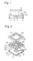
- Figs. 1 to 3 illustrate a prior art LCC type semiconductor device.
- a ceramic base 1 made of, for example, alumina is constructed from three plates, i.e. a ceramic base plate 11, a ceramic intermediate plate 12, and a ceramic top plate 13.
- the base and intermediate plates 11 and 12 have a plurality of spaced-apart half-round grooves 111 and 121 formed along the side peripheries 112 and 122 thereof.
- the width (or diameter) and the depth of the half-round grooves are 0.4 mm and 0.2 mm respectively.
- the pitch of the grooves 111 and 121 is 1.27 mm.
- metallization lines 113 and 123 are formed on the surfaces of the walls of the grooves 111 and 121.
- the base plate 11 has metallization layers or soldering pads 3 (Fig. 3) on its underside, electrically connected to the metallization lines 113.
- a metallization layer 114 is formed for receiving a semiconductor chip 2.
- the metallization layer 114 is electrically connected to a respective one of the metallization lines 113 via a metallization line 115 formed on the base plate 11.
- the intermediate plate 12 has a square aperture or cavity 124 at its central portion, corresponding to the metallization layer 114 thereunder, and a plurality of radial metallization lines 125, each of which is electrically connected to a respective one of the metallization lines 123.
- the top plate 13 has a large aperture 131 at its central portion and a metallization layer 132 for sealing a cap 5 to the ceramic body.
- the three ceramic plates 11, 12 and 13 are laminated together and fired at a high temperature to obtain a sintered ceramic body or base 1.
- the metallization lines 113 of the base plate 11 and the metallization line 123 of the intermediate plate 12 are connected to each other by the above-mentioned lamination and firing.
- the surfaces of the metallization layers 113, 114, 115, 123, 124, 125, 132 and 3 are covered with platings of nickel, gold etc.
- a semiconductor chip 2 is welded on to the exposed part of the metallization layer 114 of the centre portion of the ceramic base plate 11. Fine metal wires 4 are used for connecting the semiconductor chip 2 to respective metallization lines 125 on the intermediate plate 12.
- the cap 5 is bonded on to the metallization layer 132 of the top plate 13 with low melting point solder.
- the pitch, of the soldering pads 3 is 1.27 mm. If, for example, the number of soldering pads 3 is doubled without changing the size of the package, the pitch of the soldering pads becomes 0.635 mm.
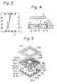
- Figs. 4 to 6 illustrate an example of a semiconductor device according to the invention.
- the device includes a semiconductor chip 2, soldering pads 3, fine wires 4 and a cap 5, as in the prior art device described above.
- a ceramic base 6 is constructed from three plates, i.e. a base plate 61, an intermediate plate 62, and a top plate 63.
- the base and intermediate plates 61 and 62 each have two sets of grooves, one being shallow and the other deep.
- the shallow grooves 611a and 621a are 0.2 mm in depth and 0.4 mm in width.
- the deep grooves 611b and 621 are 1.47 mm in depth and 0.4 mm in width.
- These two sets of grooves are arranged alternately along the side edges 612 and 622 of the base and intermediate plates 61 and 62, respectively.
- the pitch of the grooves is 0.635 mm.
- the intermediate plate 62 has a square aperture or cavity 624 at its central portion.
- the top plate 63 has a square aperture or cavity 631 at its centre and a metallization layer 632 on its upper side for bonding the cap 5 to the base 6.
- the base plate 61 has a metallization layer 614 at its central portion for receiving a semiconductor chip 2, and a metallization line 615 is directed from the metallization layer 614 to a respective one of the metallization lines 613a or 613b.
- metallization lines 613a, 613b, 623a and 623b are also formed and are connected to radial metallization lines 625 formed on the surface of the intermediate plate 62 and metallization layers or soldering pads 3 and 8 (Fig. 6) formed on the underside of the base plate 61.
- the soldering pads have a width of 0.4 mm and a length of 0.4 mm.
- the pitch of the grooves 611 and 621 is 0.635 mm
- the space between the adjacent soldering pads 3 and 8 is longer than 0.87 mm, which is as long as the space between the adjacent soldering pads 3 of the above-described prior art example having a larger pitch. Therefore, by use of the invention it is possible to increase the number of soldering pads for a given package size without increasing the risk of short circuits by solder bridges.
- FIG. 7 shows an example of an arrangement having three sets of grooves 711 a, 711 b and 711 and corresponding soldering pads 3, 8 and 9.
- the metallization layers and/or the soldering pads may be formed of tungsten, and the layers and/or the pads may be covered with a layer of gold or nickel.
Landscapes
- Engineering & Computer Science (AREA)
- Manufacturing & Machinery (AREA)
- Microelectronics & Electronic Packaging (AREA)
- Lead Frames For Integrated Circuits (AREA)
- Wire Bonding (AREA)
Claims (10)
Applications Claiming Priority (2)
| Application Number | Priority Date | Filing Date | Title |
|---|---|---|---|
| JP1982098790U JPS593549U (ja) | 1982-06-29 | 1982-06-29 | 半導体装置 |
| JP98790/82U | 1982-06-29 |
Publications (3)
| Publication Number | Publication Date |
|---|---|
| EP0098114A2 EP0098114A2 (fr) | 1984-01-11 |
| EP0098114A3 EP0098114A3 (en) | 1985-07-31 |
| EP0098114B1 true EP0098114B1 (fr) | 1988-03-02 |
Family
ID=14229157
Family Applications (1)
| Application Number | Title | Priority Date | Filing Date |
|---|---|---|---|
| EP83303642A Expired EP0098114B1 (fr) | 1982-06-29 | 1983-06-24 | Dispositif semi-conducteur à circuit intégré comprenant un support de puce sans conducteurs |
Country Status (4)
| Country | Link |
|---|---|
| EP (1) | EP0098114B1 (fr) |
| JP (1) | JPS593549U (fr) |
| DE (1) | DE3375861D1 (fr) |
| IE (1) | IE54714B1 (fr) |
Families Citing this family (5)
| Publication number | Priority date | Publication date | Assignee | Title |
|---|---|---|---|---|
| US4906802A (en) * | 1988-02-18 | 1990-03-06 | Neal Castleman | Molded chip carrier |
| FR2675632B1 (fr) * | 1991-04-18 | 1997-04-30 | Texas Instruments France | Dispositif de conditionnement de circuits integres |
| JP2537325B2 (ja) * | 1991-11-29 | 1996-09-25 | 明 北原 | 表面実装電子部品と製法 |
| JP2734284B2 (ja) * | 1992-03-25 | 1998-03-30 | 日本電気株式会社 | リードレスチップキャリア基板 |
| TWM274641U (en) * | 2005-04-01 | 2005-09-01 | Lingsen Precision Ind Ltd | Packaging carrier for integrated circuit |
Family Cites Families (1)
| Publication number | Priority date | Publication date | Assignee | Title |
|---|---|---|---|---|
| GB2056772B (en) * | 1980-08-12 | 1983-09-01 | Amdahl Corp | Integrated circuit package and module |
-
1982
- 1982-06-29 JP JP1982098790U patent/JPS593549U/ja active Pending
-
1983
- 1983-06-24 EP EP83303642A patent/EP0098114B1/fr not_active Expired
- 1983-06-24 DE DE8383303642T patent/DE3375861D1/de not_active Expired
- 1983-06-29 IE IE1529/83A patent/IE54714B1/en not_active IP Right Cessation
Also Published As
| Publication number | Publication date |
|---|---|
| DE3375861D1 (en) | 1988-04-07 |
| JPS593549U (ja) | 1984-01-11 |
| IE54714B1 (en) | 1990-01-17 |
| EP0098114A3 (en) | 1985-07-31 |
| EP0098114A2 (fr) | 1984-01-11 |
| IE831529L (en) | 1983-12-29 |
Similar Documents
| Publication | Publication Date | Title |
|---|---|---|
| JP4703980B2 (ja) | 積層型ボールグリッドアレイパッケージ及びその製造方法 | |
| US4296456A (en) | Electronic package for high density integrated circuits | |
| KR0156480B1 (ko) | 반도체 장치 및 제조방법 | |
| US5841191A (en) | Ball grid array package employing raised metal contact rings | |
| US7829990B1 (en) | Stackable semiconductor package including laminate interposer | |
| US20030205804A1 (en) | Integrated chip package structure using ceramic substrate and method of manufacturing the same | |
| US8791501B1 (en) | Integrated passive device structure and method | |
| JP7302784B2 (ja) | インターポーザ及びこれを含むパッケージ構造物 | |
| EP0027017B1 (fr) | Boitier pour un circuit intégré | |
| JPH0846079A (ja) | 半導体装置 | |
| US4538143A (en) | Light-emitting diode displayer | |
| US5790386A (en) | High I/O density MLC flat pack electronic component | |
| EP0098114A2 (fr) | Dispositif semi-conducteur à circuit intégré comprenant un support de puce sans conducteurs | |
| US12159820B2 (en) | Flat no-lead package with surface mounted structure | |
| US6384477B2 (en) | Multiple line grid array package | |
| JP3632024B2 (ja) | チップパッケージ及びその製造方法 | |
| JP2005057271A (ja) | 同一平面上に横配置された機能部及び実装部を具備する半導体チップパッケージ及びその積層モジュール | |
| JPH07321160A (ja) | 半導体装置 | |
| KR100498470B1 (ko) | 적층형 반도체 패키지 및 그 제조방법 | |
| US7361982B2 (en) | Bumpless chip package | |
| US10937707B2 (en) | Wiring substrate, electronic device, and electronic module | |
| EP0100727B1 (fr) | Dispositif semi-conducteur comprenant une base céramique | |
| US20250046516A1 (en) | Capacitor Carrier Ring And Stiffener For Integrated Circuit Package Assembly | |
| US10881006B2 (en) | Package carrier and package structure | |
| KR100243023B1 (ko) | 반도체 패키지와 그 제조방법 및 그 적층방법 |
Legal Events
| Date | Code | Title | Description |
|---|---|---|---|
| PUAI | Public reference made under article 153(3) epc to a published international application that has entered the european phase |
Free format text: ORIGINAL CODE: 0009012 |
|
| AK | Designated contracting states |
Designated state(s): DE FR GB |
|
| PUAL | Search report despatched |
Free format text: ORIGINAL CODE: 0009013 |
|
| AK | Designated contracting states |
Designated state(s): DE FR GB |
|
| 17P | Request for examination filed |
Effective date: 19860117 |
|
| 17Q | First examination report despatched |
Effective date: 19870512 |
|
| GRAA | (expected) grant |
Free format text: ORIGINAL CODE: 0009210 |
|
| AK | Designated contracting states |
Kind code of ref document: B1 Designated state(s): DE FR GB |
|
| REF | Corresponds to: |
Ref document number: 3375861 Country of ref document: DE Date of ref document: 19880407 |
|
| ET | Fr: translation filed | ||
| PLBE | No opposition filed within time limit |
Free format text: ORIGINAL CODE: 0009261 |
|
| STAA | Information on the status of an ep patent application or granted ep patent |
Free format text: STATUS: NO OPPOSITION FILED WITHIN TIME LIMIT |
|
| 26N | No opposition filed | ||
| PGFP | Annual fee paid to national office [announced via postgrant information from national office to epo] |
Ref country code: GB Payment date: 19920505 Year of fee payment: 10 |
|
| PGFP | Annual fee paid to national office [announced via postgrant information from national office to epo] |
Ref country code: FR Payment date: 19920629 Year of fee payment: 10 |
|
| PGFP | Annual fee paid to national office [announced via postgrant information from national office to epo] |
Ref country code: DE Payment date: 19920827 Year of fee payment: 10 |
|
| PG25 | Lapsed in a contracting state [announced via postgrant information from national office to epo] |
Ref country code: GB Effective date: 19930624 |
|
| GBPC | Gb: european patent ceased through non-payment of renewal fee |
Effective date: 19930624 |
|
| PG25 | Lapsed in a contracting state [announced via postgrant information from national office to epo] |
Ref country code: FR Effective date: 19940228 |
|
| PG25 | Lapsed in a contracting state [announced via postgrant information from national office to epo] |
Ref country code: DE Effective date: 19940301 |
|
| REG | Reference to a national code |
Ref country code: FR Ref legal event code: ST |