EP0098652A2 - Method of manufacturing an insulated gate field effect device and device manufactured by the method - Google Patents
Method of manufacturing an insulated gate field effect device and device manufactured by the method Download PDFInfo
- Publication number
- EP0098652A2 EP0098652A2 EP83200968A EP83200968A EP0098652A2 EP 0098652 A2 EP0098652 A2 EP 0098652A2 EP 83200968 A EP83200968 A EP 83200968A EP 83200968 A EP83200968 A EP 83200968A EP 0098652 A2 EP0098652 A2 EP 0098652A2
- Authority
- EP
- European Patent Office
- Prior art keywords
- layer
- oxidation
- silicon layer
- silicon
- gate electrode
- Prior art date
- Legal status (The legal status is an assumption and is not a legal conclusion. Google has not performed a legal analysis and makes no representation as to the accuracy of the status listed.)
- Granted
Links
Images


Classifications
-
- H—ELECTRICITY
- H10—SEMICONDUCTOR DEVICES; ELECTRIC SOLID-STATE DEVICES NOT OTHERWISE PROVIDED FOR
- H10D—INORGANIC ELECTRIC SEMICONDUCTOR DEVICES
- H10D62/00—Semiconductor bodies, or regions thereof, of devices having potential barriers
- H10D62/10—Shapes, relative sizes or dispositions of the regions of the semiconductor bodies; Shapes of the semiconductor bodies
- H10D62/13—Semiconductor regions connected to electrodes carrying current to be rectified, amplified or switched, e.g. source or drain regions
- H10D62/149—Source or drain regions of field-effect devices
- H10D62/151—Source or drain regions of field-effect devices of IGFETs
-
- H—ELECTRICITY
- H10—SEMICONDUCTOR DEVICES; ELECTRIC SOLID-STATE DEVICES NOT OTHERWISE PROVIDED FOR
- H10D—INORGANIC ELECTRIC SEMICONDUCTOR DEVICES
- H10D30/00—Field-effect transistors [FET]
- H10D30/01—Manufacture or treatment
- H10D30/021—Manufacture or treatment of FETs having insulated gates [IGFET]
- H10D30/0223—Manufacture or treatment of FETs having insulated gates [IGFET] having source and drain regions or source and drain extensions self-aligned to sides of the gate
- H10D30/0227—Manufacture or treatment of FETs having insulated gates [IGFET] having source and drain regions or source and drain extensions self-aligned to sides of the gate having both lightly-doped source and drain extensions and source and drain regions self-aligned to the sides of the gate, e.g. lightly-doped drain [LDD] MOSFET or double-diffused drain [DDD] MOSFET
-
- H—ELECTRICITY
- H10—SEMICONDUCTOR DEVICES; ELECTRIC SOLID-STATE DEVICES NOT OTHERWISE PROVIDED FOR
- H10D—INORGANIC ELECTRIC SEMICONDUCTOR DEVICES
- H10D30/00—Field-effect transistors [FET]
- H10D30/60—Insulated-gate field-effect transistors [IGFET]
-
- H—ELECTRICITY
- H10—SEMICONDUCTOR DEVICES; ELECTRIC SOLID-STATE DEVICES NOT OTHERWISE PROVIDED FOR
- H10D—INORGANIC ELECTRIC SEMICONDUCTOR DEVICES
- H10D30/00—Field-effect transistors [FET]
- H10D30/60—Insulated-gate field-effect transistors [IGFET]
- H10D30/601—Insulated-gate field-effect transistors [IGFET] having lightly-doped drain or source extensions, e.g. LDD IGFETs or DDD IGFETs
- H10D30/608—Insulated-gate field-effect transistors [IGFET] having lightly-doped drain or source extensions, e.g. LDD IGFETs or DDD IGFETs having non-planar bodies, e.g. having recessed gate electrodes
-
- H—ELECTRICITY
- H10—SEMICONDUCTOR DEVICES; ELECTRIC SOLID-STATE DEVICES NOT OTHERWISE PROVIDED FOR
- H10P—GENERIC PROCESSES OR APPARATUS FOR THE MANUFACTURE OR TREATMENT OF DEVICES COVERED BY CLASS H10
- H10P76/00—Manufacture or treatment of masks on semiconductor bodies, e.g. by lithography or photolithography
- H10P76/40—Manufacture or treatment of masks on semiconductor bodies, e.g. by lithography or photolithography of masks comprising inorganic materials
- H10P76/408—Manufacture or treatment of masks on semiconductor bodies, e.g. by lithography or photolithography of masks comprising inorganic materials characterised by their sizes, orientations, dispositions, behaviours or shapes
- H10P76/4085—Manufacture or treatment of masks on semiconductor bodies, e.g. by lithography or photolithography of masks comprising inorganic materials characterised by their sizes, orientations, dispositions, behaviours or shapes characterised by the processes involved to create the masks
Definitions
- the invention relates to a method of manufacturing an insulated gate field effect device, in which on a surface of a semiconductor region of a first conductivity type at least at the area of the gate electrode to be formed there is provided an electrically insulating layer and thereon a first silicon layer, whereupon a gate electrode is formed from the first silicon layer by etching and on either side of this electrode extensions of source and drain zones of the second opposite conductivity type are provided by implantation of ions at such an energy that at the area of the gate electrode the ions do not penetrate into the semiconductor region, and that highly doped contact portions of the source and drain zones are formed at a distance from the gate electrode determined in a self-aligning manner.
- the invention further relates to a field effect device manufactured by the method.
- IGFET insulated gate field effect transistor
- this silicon oxide is then removed everywhere except on the edges of the gate electrodew Whilst using the silicon oxide parts left behind on the edge of the gate electrode as a mask, the more highly doped contact portions of the source and drain zones are then provided down to a larger depth than the low-doped extensions so that the ultimate dimension of these low-doped parts from the source to the drain zone is determined by the width of the said silicon oxide parts.
- RIE plasma etching
- the invention has inter alia for its object to provide a method in which source and drain zone extensions having accurately reproducible very small dimensions can be obtained in a self-aligning manner in the immediate proximity of the gate electrode.
- the method can also provide a so-called buried gate electrode structure having a homogeneous gate dielectric of, for example, solely silicon oxide.
- the invention is based inter alia on the recognition of the fact that this can be achieved by the use of an auxiliary silicon layer in combination with an oxidation process.
- a method of the kind described in the preamble is characterized in that on the first silicon layer there is provided at least a first oxidation-preventing layer and thereon a second silicon layer in that then a part of the second silicon layer is removed, the edges of the remaining part of this layer substantially coinciding with the edges of the gate electrode to be provided, in that subsequently at least the edge portions of the second silicon layer are thermally oxidized in a mrst oxidation step, wnereupon the uncovered parts or the first oxidation-preventing layer are etched away selectively, in that then the oxidized edge portions are etched away and the exposed silicon surface is thermally oxidized in a second oxidation step, in that subsequently the exposed parts of the first oxidation-preventing layer are etched away and then the parts of the first silicon layer thus exposed are etched away at least down to the insulating layer, in that through the openings in the first silicon layer thus obtained, the extensions of the source and drain zones are implanted, then the exposed oxide
- a buried gate electrode structure can be obtained by the use of the method according to the invention, the gate dielectric then consisting of an insulating layer of homogeneous composition, for example, of silicon oxide.
- the gate dielectric consists of juxtaposed layers of silicon oxide and silicon nitride, which may give rise to instabilities and etching problems.
- the second silicon layer is removed at the area of the gate electrode to be formed.
- the highly doped parts of the source and drain zones can be formed by removing after the third oxidation step the remaining parts of at least the first oxidation-preventing layer and, if desired, also the underlying parts of the first silicon layer and by forming under these parts the highly doped contact portions of the source and drain zones, preferably by ion implantation, so as to join the source and drain zone extensions.
- a part of the second silicon layer is removed whilst ensuring that the part at the-area of the gate electrode to be formed remains.
- the highly doped contact portions of the source and drain zones are advantageously implanted through the first silicon layer into the semiconductor region of the first conductivity type.
- the insulating layer may be provided over the entire surface, but is often preferably provided substantially only at the area of the gate electrode to be formed.
- the second silicon layer is coated with a second oxidation-preventing layer, in which case, before removing a part of the second silicon layer, the part of the second oxidation-preventing layer disposed thereon is removed.
- the first and the second oxidation-preventing layers both preferably consist of the same material, which advantageously comprises silicon nitride.
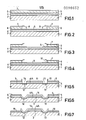
- Figures 1 to 7 diagrammatically show in cross-section successive stages in the manufacture of a first preferred embodiment of the method according to the invention.
- a surface 2 of a semiconductor region 1 of a first conductivity type in this example a p-type silicon region having a resistivity of approximately 10 ⁇ cm, for exampre, by thermal exidation an electrically insulating layer 3 of silicon oxide, on which a first silicon layer 4 is deposited.
- the silicon layer 4 is deposited in the form of a strongly n-type doped polycrystalline silicon layer from the gaseous phase by thermal decomposition of a silicon compound, such as SiH 4 , with the addition of a dopant, for example, phosphorus in the form of PH 3 , according to generally known techniques.
- a silicon compound such as SiH 4
- a dopant for example, phosphorus in the form of PH 3
- the thickness of the layer 3 is 0.05, ⁇ m and that of the layer 4 is 0.5 ⁇ m.
- a gate electrode Fig.
- n-type source and drain zone extensions 12 and 13 and highly doped n-type contact portions (15,16) of the source and drain zones, at a distance from the gate electrode determined in a self-aligning manner (see Fig.7).
- a first oxidation-preventing layer 5 is provided on the first silicon layer 4 and theron a second silicon layer 6.
- a second oxidation-preventing layer 7 is provided thereon, see Figure 1.
- the oxidation-preventing layers 5 and 7 both consist of silicon nitride, whilst the layer 6 may be a doped or an undoped polycrystalline silicon layer and may be provided in the same manner as the layer 4.
- the thickness of the layers 5 , 6 and 7 are 0.1 ⁇ m, 0.3 ⁇ m and 0.2/um, respectively. In this example, all the layers mentioned above are provided over the entire surface.
- a part of the second oxidation-preventing layer 7 and the underlying part of the second silicon layer 6 are removed by etching.
- the edges of the remaining parts of the layers 6 and 7 then substantially coincide with the edges of the gate electrode to be formed afterwards.
- hot phosphoric acid is used for selectively etching silicon nitride, and a solution of 20% by weight of KOH in water is used for selectively etching polycrystalline silicon.
- edge portions of the second silicon layer 6 are then thermally oxidized in a first oxidation step at 1000 0 C for 3 hours in water vapour, which results (see Figure 2) in that oxidized edge portions 8 having a width of approximately 0.7 ⁇ m are obtained.
- the uncovered parts of the first silicon nitride layer 5 are etched away completely and the second silicon nitride layer 7 is etched away only over part of its thickness (due to its larger thickness) without the use of an etching mask, whereupon the oxidized edge portions 8 are etched away.
- the situation shown in Figure 3 is obtained.
- the second silicon nitride layer 7 and the exposed parts of the first silicon nitride layer 5 are etched away completely, whereupon the silicon layer 6 is etched away completely and the exposed parts of the first silicon layer 4 are etched away down to the oxide layer 3, for example, in a CC1 4 -chlorine plasma at a frequency of, for example, 13.56 MHz, a pressure of 9.3 Pa and a power of 300 W.
- the gate electrode 4A and the openings 11 are then obtained, see Figure 5.
- the low-doped extensions 12 and 13 of the source and drain zones are now formed by implantation of phosphorus ions, see Figure 5.
- the energy of the implanted ions is such that at the area of the gate electrode 4A and also of the layers 4 and 5 these ions do not penetrate into the semiconductor region 1.
- the energy amounted to 100 keV
- the dose was 10 13 ions/cm 2 and the thickness of the regions 12 and 13 was 0.25 / um, whilst the implantation was carried out through the gate oxide layer 3.
- the oxide layer 3 may be removed inside the openings 11 before the implantation is carried out.
- the highly doped contact portions 15 and 16 (see Figure 7) of the source and drain zones are provided by first removing the layers 4 and 5 and, if desired, also the layer 3 by etching, and then implanting the regions 15 and 16 with phosphorus ions, the oxide layer 14 masking against this implantation, for example, at an energy of 25 keV and a dose of 5x10 15 ions/cm . If desired, the regions 15 and 16 may alternatively be obtained by diffusion.
- the regions 15 and 16 and the gate electrode 4A may be contacted in the usual manner by etching contact windows and by metallization. This is not indicated further in the figures.
- the source and drain zone portions 15 and 16 may tion in an in grated circuit conductmg semiconductor tracks and in this case need not be contacted through contact windows.
- the gate electrode may form part of a pattern of polycrystalline silicon interconnections.
- the distance of the highly doped contact portions 15 and 16 from the gate electrode 4A in other words the dimension, viewed from the source to the drain zone, of the highly doped extensions 12 and 13 in the method according to the invention is therefore fully determined in a self-aligning manner, it being fixed by the edge portions 8 oxidized earlier.
- the dimension of the parts 12 and 13 may be very small ( ⁇ 1 ⁇ m).
- a buried gate electrode 4A which is entirely surrounded by insulating material, is obtained with a gate dielectric 3, which wholly consists of silicon oxide.
- Figure 8 corresponds to the stage of Figure 4, except that the insulating layer 3, the gate dielectric, was provided here practically only at the area of the gate electrode to be formed. Further, the layers 3,4,5,6 and 7 as well as the region 1 consist of the same materials as in the preceding example, whilst the layers also have the same thicknesses.
- Figure 9 corresponds to the stage of Figure 5. Also in this case, the openings 11 were etched down to the insulating layer and the phosphorus implantation for the formation of the low-doped source and drain zone extensions 12 and 13 was carried out through the insulating layer 3, as far as this layer was present within the openings 11.
- the second oxidation-preventing silicon nitride layer 7 and the underlying part of the second silicon layer 6 were removed at the area of the gate electrode 4A to be formed.
- the following preferred embodiment illustrated with reference to Figures 12 to 17 is complementary thereto.
- a semiconductor region 1 of p-type silicon there are provided on a semiconductor region 1 of p-type silicon an insulating layer 3, the gate dielectric, arid thereon in order of succession a first silicon layer 4, a first oxidation-preventing layer 5, a second silicon layer 6 and a second oxidation-preventing layer 7.
- the layers may be of the same composition, thickness and doping as in the preceding examples.
- the insulating layer 3 is provided, like in the example shown in Figs. 8 to 11, substantially only at the area of the gate electrode to be formed.
- the layers 7 and 6 are now not removed at the area of the gate electrode to be formed, but they are just maintained at the area of the gate electrode.
- the edges of the remaining parts of the layers 6 and 7 also in this case substantially coincide with those of the gate electrode to be formed afterwards.
- the edge portions 8 of the layer 6 are oxidized whereupon the uncovered parts of the silicon nitride layer 5 are etched away completely, the silicon nitride layer 7 being removed only in part due to its larger thickness.
- the highly doped contact portions 15 and 16 of the source and drain zones are then implanted through the first silicon layer 4 (and the layer 3) by means of an implantation of phosphorus ions, which are masked by the layers 5,6,8 and 7.
- the structure of Figure 13 is obtained.
- the structure of Figure 4 is obtained.
- the oxide layers 9 and 10 are then formed, see Figure 15.
- the openings 11 are obtained (see Figure 16).
- the low-doped source and drain zone extensions 12 and 13 are then formed.
- a third oxidation step is carried out so as to produce the oxide layer 14.
- the gate electrode 4A is not entirely surrounded by oxide, but is covered on the upper side by the silicon nitride layer 5. However, when this layer 5 is etched away before the oxide layer 14 is formed, a buried gate electrode structure analogous to that of Figures 7 and 11 is obtained.
- source and drain zones may be contacted in the usual manner by etching contact windows and metallizing.
- FIG. 1 to 7 The presence of a second oxidation-preventing layer 7 is not always required.
- the method shown in Figures 1 to 7 may be carried out in the absence of layer 7. for father explanation see Figures 18 to 22, which correspond to the respective Figures 1 to 5, in case the layer 7 is omitted.
- Figure 19 during the first oxidation step the edge portions of the second silicon layer 6 are converted completely into oxide 8, the remaining parts of the layer 6 being converted into oxide 8A over only part of their thickness. If the remaining part of the silicon layer 6 is sufficiently thin, the part of the silicon layer 6 left after etching away the oxide (8,8A) is converted completely into oxide 10 during the second oxidation step (see Figure 21).
- the method is terminated in the manner shown in Figures 6 and 7.
- the method shown in Figures 12 to 17 may be carried out in the absence of layer 7. See Figures 23 to 27, which correspond to the respective Figures 12 to 17 in the absence of layer 7.
- a part 8A of the remaining part of the layer 6 outside the edge portions 8 is likewise converted into oxide. If the remaining part of layer 6 is sufficiently thin, it is oxidized completely during the second oxidation step ( Figure 26).
- the method is terminated by the steps shown in Figures 16 and 17.
- the first oxidation step must be accurately controlled since outside the edge portions 8 the silicon layer 6 should be oxidized over only part of its thickness. Therefore, the use of a second oxidation-preventing layer 7 may sometimes be advantageous.
- the silicon nitride layer 7 may be as thick as or thinner than the silicon nitride layer 5.
- the layer 7 is then etched away completely in the stage of Figure 3, whilst during the second oxidation step ( Figure 4) the thin silicon layer 6 is oxidized completely.
- the method may be terminated by the same steps as in Figures 5 to 7. The same modification may of course be applied to the example of Figures 12 to 17.
- the semiconductor region 1 may consist of another semiconductor material than silicon.
- the oxidation-preventing layers 5 and 7 may instead of silicon nitride comprise silicon oxynitride or another oxidation-preventing material.
- the layers 5 and 6 need even not consist of the same material (although this would result in an increase of the number of etching steps).
- the thickness of the layers 4,5,6 and 7 may be suitably chosen for each application by those skilled in the art.
- the gate dielectric 3 may consist of another material than silicon oxide.
- an additional mask When an additional mask is used, another implantation dose may be utilized for the formation of the region 12 than for the formation of the region 13. This is of importance when, for example, only the drain zone, but not the source zone is to be provided with a comparatively low-doped extension 13.
- the extension 12 may then be chosen to be more highly doped and/or thicker than the region 13.
- the use of an additional mask is only possible with somewhat larger dimensions.
- n-channel MOS transistors of the enhancement type were realized, p-channel transistors may be manufactured by reversal of all conductivity types and by implantation of acceptor ions, for example, boron ions.
- depletion transistors may be manufactured by implanting or diffusing an n- or a p-type channel at the area of the gate electrode to be formed before the layer 3 is provided.
- a plurality of gate electrodes may be realized for the formation of, for example, a tetrode-MOST or a charge-coupled device (CCD).
Landscapes
- Insulated Gate Type Field-Effect Transistor (AREA)
- Electrodes Of Semiconductors (AREA)
Abstract
Description
- The invention relates to a method of manufacturing an insulated gate field effect device, in which on a surface of a semiconductor region of a first conductivity type at least at the area of the gate electrode to be formed there is provided an electrically insulating layer and thereon a first silicon layer, whereupon a gate electrode is formed from the first silicon layer by etching and on either side of this electrode extensions of source and drain zones of the second opposite conductivity type are provided by implantation of ions at such an energy that at the area of the gate electrode the ions do not penetrate into the semiconductor region, and that highly doped contact portions of the source and drain zones are formed at a distance from the gate electrode determined in a self-aligning manner.
- The invention further relates to a field effect device manufactured by the method.
- A method of the kind described above is known from the "Proceedings of the International Electronic Device Meeting" (IEDM) 1981, Paper 28.3 of Ogura et al, "Elimination of hot electron gate currents by the lightly doped drain-source structure", p. 651-654.
- In field effect devices, such as, for example, an insulated gate field effect transistor (IGFET), it is desirable in certain cases that at least the drain zone in the immediate proximity of the gate electrode has a lower-doped extension, whilst the remaining part of the drain zone is constituted by a more highly doped contact portion, which is located at a small distance from the gate electrode. As a result, the breakdown voltage of the drain/pn-junction is increased and injection of hot charge carriers into the gate dielectric resulting in a degradation of the characteristics is prevented. This is of particular importance in field effect devices having a very small channel length, in which the influence on the characteristics of injection of hot charge carriers into the gate dielectric is relatively greatest.
- However, in particular at very small dimensions, technological difficulties are involved in providing such extensions of the source and/ or drain zones. Extensions of source and drain zones having a dimension of 1 µm or less between the gate electrode and the highly doped contact portion cannot or can hardly be formed in a reproducible manner with the aid of masking techniques, due to the alignment tolerance then required.
- In the said publication in IEDM 1981, a method is described of manufacturing an insulated gate field effect transistor in which, after the gate electrode consisting of polycrystalline silicon has been defined, low-doped source and drain zone extensions are implanted whilst using the gate electrode as a mask. Subsequently, a layer of silicon oxide is pyrolytically deposited on the whole surface, inclusive of the gate electrode. By means of plasma etching (RIE), this silicon oxide is then removed everywhere except on the edges of the gate electrodew Whilst using the silicon oxide parts left behind on the edge of the gate electrode as a mask, the more highly doped contact portions of the source and drain zones are then provided down to a larger depth than the low-doped extensions so that the ultimate dimension of these low-doped parts from the source to the drain zone is determined by the width of the said silicon oxide parts.
- This known method has several important disadvantages. For example, the width of the silicon oxide parts left behind on the edge of the gate electrode is poorly reproducible. Further, the plasma etching treatment of the pyrolytically deposited oxide is not selective with respect to the underlying gate oxide so that the etching process cannot be controlled easily.
- The invention has inter alia for its object to provide a method in which source and drain zone extensions having accurately reproducible very small dimensions can be obtained in a self-aligning manner in the immediate proximity of the gate electrode. The method can also provide a so-called buried gate electrode structure having a homogeneous gate dielectric of, for example, solely silicon oxide.
- The invention is based inter alia on the recognition of the fact that this can be achieved by the use of an auxiliary silicon layer in combination with an oxidation process.
- According to the invention, a method of the kind described in the preamble is characterized in that on the first silicon layer there is provided at least a first oxidation-preventing layer and thereon a second silicon layer in that then a part of the second silicon layer is removed, the edges of the remaining part of this layer substantially coinciding with the edges of the gate electrode to be provided, in that subsequently at least the edge portions of the second silicon layer are thermally oxidized in a mrst oxidation step, wnereupon the uncovered parts or the first oxidation-preventing layer are etched away selectively, in that then the oxidized edge portions are etched away and the exposed silicon surface is thermally oxidized in a second oxidation step, in that subsequently the exposed parts of the first oxidation-preventing layer are etched away and then the parts of the first silicon layer thus exposed are etched away at least down to the insulating layer, in that through the openings in the first silicon layer thus obtained, the extensions of the source and drain zones are implanted, then the exposed oxide layers are etched away and in that during a third oxidation step the silicon thus exposed is provided with a thermal oxide layer.
- By the use of the method according to the invention, source and drain zone extensions with accurately defined and controllable dimensions are obtained. In this connection, it is of great importance that the step of etching the silicon layer is very selective with respect to the underlying gate dielectric (the insulating layer) and as a result can be very accurately controlled.
- Alternatively, as has already been stated, a buried gate electrode structure can be obtained by the use of the method according to the invention, the gate dielectric then consisting of an insulating layer of homogeneous composition, for example, of silicon oxide. This in contrast with most of the known techniques for obtaining buried gate electrode structures, in which mostly the gate dielectric consists of juxtaposed layers of silicon oxide and silicon nitride, which may give rise to instabilities and etching problems.
- According to a first preferred embodiment, the second silicon layer is removed at the area of the gate electrode to be formed. In this preferred embodiment, the highly doped parts of the source and drain zones can be formed by removing after the third oxidation step the remaining parts of at least the first oxidation-preventing layer and, if desired, also the underlying parts of the first silicon layer and by forming under these parts the highly doped contact portions of the source and drain zones, preferably by ion implantation, so as to join the source and drain zone extensions.
- According to a second preferred embodiment, a part of the second silicon layer is removed whilst ensuring that the part at the-area of the gate electrode to be formed remains. In this preferred embodiment, after the first oxidation-preventing layer has been etched away and before the pxidized edge portions are etched away, the highly doped contact portions of the source and drain zones are advantageously implanted through the first silicon layer into the semiconductor region of the first conductivity type.
- The insulating layer may be provided over the entire surface, but is often preferably provided substantially only at the area of the gate electrode to be formed.
- According to a further important preferred embodiment, the second silicon layer is coated with a second oxidation-preventing layer, in which case, before removing a part of the second silicon layer, the part of the second oxidation-preventing layer disposed thereon is removed. The first and the second oxidation-preventing layers both preferably consist of the same material, which advantageously comprises silicon nitride.
- The invention will now be described more fully with reference to a few embodiments and the drawing, in which:
- Figures 1 to 7 diagrammatically show in cross-section successive stages in the manufacture of a first preferred embodiment of the method according to the invention,
- Figures 8 to 11 show a modification of the method shown in Figures 1 to 7,
- Figures 12 to 17 diagrammatically show in cross-section another preferred embodiment of the method according to the invention in successive stages of manufacture,
- Figures 18 to 22 show a further modification of the method shown in Figs. 1 to 7, and
- Figures 23 to 27 show a modification of the method shown in Figs. 12 to 17.
- The figures are purely schematic and not drawn to scale. This applies in particular to the dimensions in the direction of thickness. Corresponding parts are generally designated by the same reference numerals. Semiconductor regions of the same conductivity type are generally cross-hatched in the same direction.
- Figures 1 to 7 diagrammatically show in cross-section successive stages in the manufacture of a first preferred embodiment of the method according to the invention. As is indicated in Figure 1, there is first provided cn a
surface 2 of asemiconductor region 1 of a first conductivity type, in this example a p-type silicon region having a resistivity of approximately 10Ωcm, for exampre, by thermal exidation an electrically insulatinglayer 3 of silicon oxide, on which afirst silicon layer 4 is deposited. In this example, thesilicon layer 4 is deposited in the form of a strongly n-type doped polycrystalline silicon layer from the gaseous phase by thermal decomposition of a silicon compound, such as SiH4, with the addition of a dopant, for example, phosphorus in the form of PH3, according to generally known techniques. The thickness of thelayer 3 is 0.05,µm and that of thelayer 4 is 0.5 µm. As will be described below in greater detail, a gate electrode (Fig. 5) will be formed from the saidfirst silicon layer 4 by etching, whilst on either side of this electrode, there are formed by ion implantation n-type source anddrain zone extensions - According to the invention, for this purpose a first oxidation-preventing
layer 5 is provided on thefirst silicon layer 4 and theron asecond silicon layer 6. In this example, moreover a second oxidation-preventinglayer 7 is provided thereon, see Figure 1. In this example, the oxidation-preventinglayers layer 6 may be a doped or an undoped polycrystalline silicon layer and may be provided in the same manner as thelayer 4. The thickness of thelayers - Subsequently (see Figure 2), a part of the second oxidation-preventing
layer 7 and the underlying part of thesecond silicon layer 6 are removed by etching. The edges of the remaining parts of thelayers - The edge portions of the
second silicon layer 6 are then thermally oxidized in a first oxidation step at 10000C for 3 hours in water vapour, which results (see Figure 2) in that oxidizededge portions 8 having a width of approximately 0.7µm are obtained. Subsequently, the uncovered parts of the firstsilicon nitride layer 5 are etched away completely and the secondsilicon nitride layer 7 is etched away only over part of its thickness (due to its larger thickness) without the use of an etching mask, whereupon the oxidizededge portions 8 are etched away. Thus, the situation shown in Figure 3 is obtained. - During a second oxidation step at 850°C for 90 minutes in water vapour, the silicon surface now exposed is thermally oxidized. The
oxide layer 9 is then formed, whilst also the edge portions of thesilicon layer 6 are lightly oxidized, which results in thatoxide layers 10 are obtained, see Figure 4. - Subsequently, the second
silicon nitride layer 7 and the exposed parts of the firstsilicon nitride layer 5 are etched away completely, whereupon thesilicon layer 6 is etched away completely and the exposed parts of thefirst silicon layer 4 are etched away down to theoxide layer 3, for example, in a CC14-chlorine plasma at a frequency of, for example, 13.56 MHz, a pressure of 9.3 Pa and a power of 300 W. Thegate electrode 4A and theopenings 11 are then obtained, see Figure 5. - Through the
openings 11, the low-dopedextensions gate electrode 4A and also of thelayers semiconductor region 1. In this example, the energy amounted to 100 keV, the dose was 1013 ions/cm2 and the thickness of theregions gate oxide layer 3. However, if desired, theoxide layer 3 may be removed inside theopenings 11 before the implantation is carried out. - All the exposed oxide layers are then removed by etching, whereupon during a third oxidation step at 850°C for 300 min. in water vapour the silicon thus exposed is provided with a
thermal oxide layer 14, see Figure 6. - In this example, the highly doped
contact portions 15 and 16 (see Figure 7) of the source and drain zones are provided by first removing thelayers layer 3 by etching, and then implanting theregions oxide layer 14 masking against this implantation, for example, at an energy of 25 keV and a dose of 5x10¹⁵ ions/cm . If desired, theregions - The
regions gate electrode 4A may be contacted in the usual manner by etching contact windows and by metallization. This is not indicated further in the figures. The source and drainzone portions - The distance of the highly doped
contact portions gate electrode 4A, in other words the dimension, viewed from the source to the drain zone, of the highly dopedextensions edge portions 8 oxidized earlier. The dimension of theparts gate electrode 4A, which is entirely surrounded by insulating material, is obtained with agate dielectric 3, which wholly consists of silicon oxide. - A modification of this preferred embodiment is now described with reference to Figures 8 to 11, in which the reference numerals correspond to those of Figs. 1 to 7. Figure 8 corresponds to the stage of Figure 4, except that the insulating
layer 3, the gate dielectric, was provided here practically only at the area of the gate electrode to be formed. Further, thelayers region 1 consist of the same materials as in the preceding example, whilst the layers also have the same thicknesses. - Figure 9 corresponds to the stage of Figure 5. Also in this case, the
openings 11 were etched down to the insulating layer and the phosphorus implantation for the formation of the low-doped source and drainzone extensions layer 3, as far as this layer was present within theopenings 11. - The stages of Figures 10 and 11 correspond to those of Figures 6 and 7. In this case, however, the highly doped source and drain
contact regions first silicon layer 4. The parts of thelayer 4 thus strongly n-type doped likewise form part of the highly doped contact portions of the source and drain zones. - In the two preceding examples, the second oxidation-preventing
silicon nitride layer 7 and the underlying part of thesecond silicon layer 6 were removed at the area of thegate electrode 4A to be formed. The following preferred embodiment illustrated with reference to Figures 12 to 17 is complementary thereto. - Like in the preceding examples, there are provided on a
semiconductor region 1 of p-type silicon an insulatinglayer 3, the gate dielectric, arid thereon in order of succession afirst silicon layer 4, a first oxidation-preventinglayer 5, asecond silicon layer 6 and a second oxidation-preventinglayer 7. The layers may be of the same composition, thickness and doping as in the preceding examples. The insulatinglayer 3 is provided, like in the example shown in Figs. 8 to 11, substantially only at the area of the gate electrode to be formed. - In contrast with the preceding examples, however, the
layers layers edge portions 8 of thelayer 6 are oxidized whereupon the uncovered parts of thesilicon nitride layer 5 are etched away completely, thesilicon nitride layer 7 being removed only in part due to its larger thickness. The highlydoped contact portions layers - After selectively etching away the oxidized
edge portions 8, the structure of Figure 4 is obtained. During a second oxidation step, theoxide layers silicon nitride layers second silicon layer 6 and the exposed parts of thefirst silicon layer 4 down to the insulatinglayer 3, theopenings 11 are obtained (see Figure 16). By implantation of phosphorus ions, the low-doped source and drainzone extensions oxide layer 14. In this case , thegate electrode 4A is not entirely surrounded by oxide, but is covered on the upper side by thesilicon nitride layer 5. However, when thislayer 5 is etched away before theoxide layer 14 is formed, a buried gate electrode structure analogous to that of Figures 7 and 11 is obtained. - Again the source and drain zones may be contacted in the usual manner by etching contact windows and metallizing.
- The presence of a second oxidation-preventing
layer 7 is not always required. Thus, the method shown in Figures 1 to 7 may be carried out in the absence oflayer 7. for father explanation see Figures 18 to 22, which correspond to the respective Figures 1 to 5, in case thelayer 7 is omitted. In this case (see Figure 19), during the first oxidation step the edge portions of thesecond silicon layer 6 are converted completely intooxide 8, the remaining parts of thelayer 6 being converted intooxide 8A over only part of their thickness. If the remaining part of thesilicon layer 6 is sufficiently thin, the part of thesilicon layer 6 left after etching away the oxide (8,8A) is converted completely intooxide 10 during the second oxidation step (see Figure 21). After theopenings 11 have been etched, the method is terminated in the manner shown in Figures 6 and 7. In an analogous manner, the method shown in Figures 12 to 17 may be carried out in the absence oflayer 7. See Figures 23 to 27, which correspond to the respective Figures 12 to 17 in the absence oflayer 7. Here too, during the first oxidation step (see Figure 24) apart 8A of the remaining part of thelayer 6 outside theedge portions 8 is likewise converted into oxide. If the remaining part oflayer 6 is sufficiently thin, it is oxidized completely during the second oxidation step (Figure 26). After theopenings 11 have been etched, the method is terminated by the steps shown in Figures 16 and 17. - When a second oxidation-preventing
layer 7 is not used, the first oxidation step must be accurately controlled since outside theedge portions 8 thesilicon layer 6 should be oxidized over only part of its thickness. Therefore, the use of a second oxidation-preventinglayer 7 may sometimes be advantageous. - If the
second silicon layer 6 is sufficiently thin, for example, thinner than 50 nm, in the embodiment of Figs. 1 to 7 thesilicon nitride layer 7 may be as thick as or thinner than thesilicon nitride layer 5. Thelayer 7 is then etched away completely in the stage of Figure 3, whilst during the second oxidation step (Figure 4) thethin silicon layer 6 is oxidized completely. The method may be terminated by the same steps as in Figures 5 to 7. The same modification may of course be applied to the example of Figures 12 to 17. - It should be appreciated that many further modifications are possible within the scope of the invention. For example, the
semiconductor region 1 may consist of another semiconductor material than silicon. Furthermore, the oxidation-preventinglayers layers layers gate dielectric 3 may consist of another material than silicon oxide. - When an additional mask is used, another implantation dose may be utilized for the formation of the
region 12 than for the formation of theregion 13. This is of importance when, for example, only the drain zone, but not the source zone is to be provided with a comparatively low-dopedextension 13. Theextension 12 may then be chosen to be more highly doped and/or thicker than theregion 13. The use of an additional mask, however, is only possible with somewhat larger dimensions. - Although in the given embodiments, n-channel MOS transistors of the enhancement type were realized, p-channel transistors may be manufactured by reversal of all conductivity types and by implantation of acceptor ions, for example, boron ions. Furthermore, instead of enhancement transistors, depletion transistors may be manufactured by implanting or diffusing an n- or a p-type channel at the area of the gate electrode to be formed before the
layer 3 is provided. Instead of one gate electrode, a plurality of gate electrodes may be realized for the formation of, for example, a tetrode-MOST or a charge-coupled device (CCD).
Claims (15)
Applications Claiming Priority (2)
| Application Number | Priority Date | Filing Date | Title |
|---|---|---|---|
| NL8202686 | 1982-07-05 | ||
| NL8202686A NL8202686A (en) | 1982-07-05 | 1982-07-05 | METHOD FOR MANUFACTURING A FIELD-EFFECTING DEVICE WITH INSULATED CONTROL ELECTRODE, AND DEVICE MADE ACCORDING TO THE METHOD |
Publications (3)
| Publication Number | Publication Date |
|---|---|
| EP0098652A2 true EP0098652A2 (en) | 1984-01-18 |
| EP0098652A3 EP0098652A3 (en) | 1984-02-22 |
| EP0098652B1 EP0098652B1 (en) | 1986-09-17 |
Family
ID=19839970
Family Applications (1)
| Application Number | Title | Priority Date | Filing Date |
|---|---|---|---|
| EP83200968A Expired EP0098652B1 (en) | 1982-07-05 | 1983-06-29 | Method of manufacturing an insulated gate field effect device and device manufactured by the method |
Country Status (6)
| Country | Link |
|---|---|
| US (1) | US4545110A (en) |
| EP (1) | EP0098652B1 (en) |
| JP (1) | JPS5922366A (en) |
| CA (1) | CA1206625A (en) |
| DE (1) | DE3366266D1 (en) |
| NL (1) | NL8202686A (en) |
Cited By (11)
| Publication number | Priority date | Publication date | Assignee | Title |
|---|---|---|---|---|
| EP0132009A3 (en) * | 1983-07-15 | 1985-03-13 | N.V. Philips' Gloeilampenfabrieken | Method of manufacturing a semiconductor device and semiconductor device manufactured by means of the method |
| EP0158371A1 (en) * | 1984-01-25 | 1985-10-16 | Koninklijke Philips Electronics N.V. | Method of manufacturing a semiconductor device and device manufactured by the use of the method |
| EP0171105A3 (en) * | 1984-07-13 | 1986-02-19 | N.V. Philips' Gloeilampenfabrieken | Method of manufacturing a semiconductor device and device manufactured by the use of the method |
| EP0178000A3 (en) * | 1984-09-18 | 1986-04-23 | N.V. Philips' Gloeilampenfabrieken | Method of forming submicron grooves in, for example, semiconductor material and devices obtained by means of this method |
| EP0181812A1 (en) * | 1984-11-06 | 1986-05-21 | Thomson-Csf | Process for making a gate structure for integrated circuits |
| GB2172743A (en) * | 1985-03-23 | 1986-09-24 | Stc Plc | Forming gate sidewall oxide spacers |
| US4653173A (en) * | 1985-03-04 | 1987-03-31 | Signetics Corporation | Method of manufacturing an insulated gate field effect device |
| EP0300514A1 (en) * | 1987-03-18 | 1989-01-25 | Koninklijke Philips Electronics N.V. | Semiconductor device with a sidelong contact structure, and its manufacture |
| GB2215515A (en) * | 1988-03-14 | 1989-09-20 | Philips Electronic Associated | A lateral insulated gate field effect transistor and a method of manufacture |
| EP0452720A3 (en) * | 1990-04-02 | 1994-10-26 | Nat Semiconductor Corp | A semiconductor structure and method of its manufacture |
| EP0730309A1 (en) * | 1995-02-21 | 1996-09-04 | STMicroelectronics S.r.l. | A high voltage MOSFET structure with field plate electrode and process for its fabrication |
Families Citing this family (9)
| Publication number | Priority date | Publication date | Assignee | Title |
|---|---|---|---|---|
| JPS61140122A (en) * | 1984-12-13 | 1986-06-27 | Mitsubishi Electric Corp | On-load tap changer |
| US4649629A (en) * | 1985-07-29 | 1987-03-17 | Thomson Components - Mostek Corp. | Method of late programming a read only memory |
| JPS63262873A (en) * | 1987-04-21 | 1988-10-31 | Fuji Xerox Co Ltd | Semiconductor device |
| JPH0258206A (en) * | 1988-08-23 | 1990-02-27 | Mitsubishi Electric Corp | On-load tap changer |
| US5039621A (en) * | 1990-06-08 | 1991-08-13 | Texas Instruments Incorporated | Semiconductor over insulator mesa and method of forming the same |
| US5888873A (en) * | 1996-11-06 | 1999-03-30 | Advanced Micro Devices, Inc. | Method of manufacturing short channel MOS devices |
| US6525340B2 (en) * | 2001-06-04 | 2003-02-25 | International Business Machines Corporation | Semiconductor device with junction isolation |
| US7166867B2 (en) * | 2003-12-05 | 2007-01-23 | International Rectifier Corporation | III-nitride device with improved layout geometry |
| JP2006275124A (en) * | 2005-03-29 | 2006-10-12 | Shinwa Sangyo Co Ltd | Gas cock for city gas |
Family Cites Families (6)
| Publication number | Priority date | Publication date | Assignee | Title |
|---|---|---|---|---|
| JPS5284981A (en) * | 1976-01-06 | 1977-07-14 | Mitsubishi Electric Corp | Production of insulated gate type semiconductor device |
| JPS54140483A (en) * | 1978-04-21 | 1979-10-31 | Nec Corp | Semiconductor device |
| US4173818A (en) * | 1978-05-30 | 1979-11-13 | International Business Machines Corporation | Method for fabricating transistor structures having very short effective channels |
| JPS5621372A (en) * | 1979-07-31 | 1981-02-27 | Fujitsu Ltd | Manufacture of semiconductor device |
| NL187328C (en) * | 1980-12-23 | 1991-08-16 | Philips Nv | METHOD FOR MANUFACTURING A SEMICONDUCTOR DEVICE |
| US4419809A (en) * | 1981-12-30 | 1983-12-13 | International Business Machines Corporation | Fabrication process of sub-micrometer channel length MOSFETs |
-
1982
- 1982-07-05 NL NL8202686A patent/NL8202686A/en not_active Application Discontinuation
-
1983
- 1983-06-29 EP EP83200968A patent/EP0098652B1/en not_active Expired
- 1983-06-29 DE DE8383200968T patent/DE3366266D1/en not_active Expired
- 1983-06-30 CA CA000431567A patent/CA1206625A/en not_active Expired
- 1983-07-04 JP JP58120420A patent/JPS5922366A/en active Pending
-
1984
- 1984-09-07 US US06/648,603 patent/US4545110A/en not_active Expired - Fee Related
Non-Patent Citations (5)
| Title |
|---|
| IBM TECHNICAL DISCLOSURE BULLETIN, vol. 21, no. 12, May 1979, pages 5035-5038, New York, USA; E. BASSOUS et al.: "Method of fabricating high-performance IGFET structures with highly controllable submicron effective channel lengths". * |
| IBM TECHNICAL DISCLOSURE BULLETIN, vol. 22, no. 8B, January 1980, pages 3688-3690, New York, USA; R.C. VARSHNEY: "Polysilicon oxide process for small line gaps". * |
| NEUES AUS DER TECHNIK, no. 1, 15th February 1980, page 3, Würzburg, DE; "Doppelschichtmetallisierung im "buried gate"-Verfahren". * |
| NEUES AUS DER TECHNIK, no. 2, 15th April 1980, page 3, Würzburg, DE; "Herstellung kleiner MOS-Transistoren". * |
| Proc. IEDM-81, pp. 651-654 * |
Cited By (16)
| Publication number | Priority date | Publication date | Assignee | Title |
|---|---|---|---|---|
| EP0132009A3 (en) * | 1983-07-15 | 1985-03-13 | N.V. Philips' Gloeilampenfabrieken | Method of manufacturing a semiconductor device and semiconductor device manufactured by means of the method |
| EP0158371A1 (en) * | 1984-01-25 | 1985-10-16 | Koninklijke Philips Electronics N.V. | Method of manufacturing a semiconductor device and device manufactured by the use of the method |
| EP0171105A3 (en) * | 1984-07-13 | 1986-02-19 | N.V. Philips' Gloeilampenfabrieken | Method of manufacturing a semiconductor device and device manufactured by the use of the method |
| EP0178000A3 (en) * | 1984-09-18 | 1986-04-23 | N.V. Philips' Gloeilampenfabrieken | Method of forming submicron grooves in, for example, semiconductor material and devices obtained by means of this method |
| EP0181812A1 (en) * | 1984-11-06 | 1986-05-21 | Thomson-Csf | Process for making a gate structure for integrated circuits |
| FR2573919A1 (en) * | 1984-11-06 | 1986-05-30 | Thomson Csf | METHOD OF MANUFACTURING GRIDS FOR INTEGRATED CIRCUIT |
| US4738683A (en) * | 1984-11-06 | 1988-04-19 | Thomson-Csf | Method of fabrication of gates for integrated circuits |
| EP0193992A3 (en) * | 1985-03-04 | 1988-03-23 | N.V. Philips' Gloeilampenfabrieken | Method of manufacturing an insulated gate field effect device and device manufactured by the method |
| US4653173A (en) * | 1985-03-04 | 1987-03-31 | Signetics Corporation | Method of manufacturing an insulated gate field effect device |
| GB2172743A (en) * | 1985-03-23 | 1986-09-24 | Stc Plc | Forming gate sidewall oxide spacers |
| EP0300514A1 (en) * | 1987-03-18 | 1989-01-25 | Koninklijke Philips Electronics N.V. | Semiconductor device with a sidelong contact structure, and its manufacture |
| GB2215515A (en) * | 1988-03-14 | 1989-09-20 | Philips Electronic Associated | A lateral insulated gate field effect transistor and a method of manufacture |
| EP0452720A3 (en) * | 1990-04-02 | 1994-10-26 | Nat Semiconductor Corp | A semiconductor structure and method of its manufacture |
| US5661046A (en) * | 1990-04-02 | 1997-08-26 | National Semiconductor Corporation | Method of fabricating BiCMOS device |
| EP0730309A1 (en) * | 1995-02-21 | 1996-09-04 | STMicroelectronics S.r.l. | A high voltage MOSFET structure with field plate electrode and process for its fabrication |
| US6093588A (en) * | 1995-02-21 | 2000-07-25 | Stmicroelectronics, S.R.L. | Process for fabricating a high voltage MOSFET |
Also Published As
| Publication number | Publication date |
|---|---|
| CA1206625A (en) | 1986-06-24 |
| JPS5922366A (en) | 1984-02-04 |
| US4545110A (en) | 1985-10-08 |
| EP0098652A3 (en) | 1984-02-22 |
| EP0098652B1 (en) | 1986-09-17 |
| DE3366266D1 (en) | 1986-10-23 |
| NL8202686A (en) | 1984-02-01 |
Similar Documents
| Publication | Publication Date | Title |
|---|---|---|
| EP0098652B1 (en) | Method of manufacturing an insulated gate field effect device and device manufactured by the method | |
| US5861334A (en) | Method for fabricating semiconductor device having a buried channel | |
| US5384279A (en) | Method of manufacturing a semiconductor device comprising a silicon body in which semiconductor regions are formed by ion implantations | |
| US4703551A (en) | Process for forming LDD MOS/CMOS structures | |
| KR100392901B1 (en) | Method of manufacturing an asymmetric slightly doped drain (LCD) MOS device | |
| US6426279B1 (en) | Epitaxial delta doping for retrograde channel profile | |
| KR970011744B1 (en) | Mosfet of ldd type and a method for fabricating the same | |
| EP0198335B1 (en) | Graded extended drain concept for reduced hot electron effect | |
| US5714393A (en) | Diode-connected semiconductor device and method of manufacture | |
| US5635749A (en) | High performance field effect transistor with lai region | |
| US5970338A (en) | Method of producing an EEPROM semiconductor structure | |
| US6150698A (en) | Semiconductor device and method of forming semiconductor device having non-uniformly doped well | |
| US4859620A (en) | Graded extended drain concept for reduced hot electron effect | |
| EP0198336B1 (en) | Hybrid extended drain concept for reduced hot electron effect | |
| US4229756A (en) | Ultra high speed complementary MOS device | |
| US6077736A (en) | Method of fabricating a semiconductor device | |
| KR100368847B1 (en) | Insulated gate semiconductor device and its manufacturing method | |
| US5482888A (en) | Method of manufacturing a low resistance, high breakdown voltage, power MOSFET | |
| KR100211635B1 (en) | Semiconductor device and manufacturing method | |
| EP0337823A2 (en) | MOS field effect transistor having high breakdown voltage | |
| JPH0244154B2 (en) | ||
| US5895243A (en) | Semiconductor processing method of providing electrical isolation between adjacent semiconductor diffusion regions of different field effect transistors and integrated circuitry having adjacent electrically isolated field effect transistors | |
| CN1238564A (en) | Insulated gate transistor, method of manufacturing same, and semiconductor integrated circuit device | |
| KR19990051079A (en) | Manufacturing Method of Power Device Using Insulating Film Inclined Etching | |
| US5970347A (en) | High performance mosfet transistor fabrication technique |
Legal Events
| Date | Code | Title | Description |
|---|---|---|---|
| PUAI | Public reference made under article 153(3) epc to a published international application that has entered the european phase |
Free format text: ORIGINAL CODE: 0009012 |
|
| PUAL | Search report despatched |
Free format text: ORIGINAL CODE: 0009013 |
|
| AK | Designated contracting states |
Designated state(s): DE FR GB NL |
|
| AK | Designated contracting states |
Designated state(s): DE FR GB NL |
|
| 17P | Request for examination filed |
Effective date: 19840308 |
|
| GRAA | (expected) grant |
Free format text: ORIGINAL CODE: 0009210 |
|
| AK | Designated contracting states |
Kind code of ref document: B1 Designated state(s): DE FR GB NL |
|
| REF | Corresponds to: |
Ref document number: 3366266 Country of ref document: DE Date of ref document: 19861023 |
|
| ET | Fr: translation filed | ||
| PLBE | No opposition filed within time limit |
Free format text: ORIGINAL CODE: 0009261 |
|
| STAA | Information on the status of an ep patent application or granted ep patent |
Free format text: STATUS: NO OPPOSITION FILED WITHIN TIME LIMIT |
|
| 26N | No opposition filed | ||
| PGFP | Annual fee paid to national office [announced via postgrant information from national office to epo] |
Ref country code: NL Payment date: 19900630 Year of fee payment: 8 |
|
| PGFP | Annual fee paid to national office [announced via postgrant information from national office to epo] |
Ref country code: GB Payment date: 19910603 Year of fee payment: 9 |
|
| PGFP | Annual fee paid to national office [announced via postgrant information from national office to epo] |
Ref country code: FR Payment date: 19910621 Year of fee payment: 9 |
|
| PGFP | Annual fee paid to national office [announced via postgrant information from national office to epo] |
Ref country code: DE Payment date: 19910823 Year of fee payment: 9 |
|
| PG25 | Lapsed in a contracting state [announced via postgrant information from national office to epo] |
Ref country code: NL Effective date: 19920101 |
|
| NLV4 | Nl: lapsed or anulled due to non-payment of the annual fee | ||
| PG25 | Lapsed in a contracting state [announced via postgrant information from national office to epo] |
Ref country code: GB Effective date: 19920629 |
|
| GBPC | Gb: european patent ceased through non-payment of renewal fee |
Effective date: 19920629 |
|
| PG25 | Lapsed in a contracting state [announced via postgrant information from national office to epo] |
Ref country code: FR Effective date: 19930226 |
|
| PG25 | Lapsed in a contracting state [announced via postgrant information from national office to epo] |
Ref country code: DE Effective date: 19930302 |
|
| REG | Reference to a national code |
Ref country code: FR Ref legal event code: ST |