EP0099193B1 - Processeur de signaux d'ondes optiques guidées pour multiplication matrice-vecteur et pour filtrage - Google Patents
Processeur de signaux d'ondes optiques guidées pour multiplication matrice-vecteur et pour filtrage Download PDFInfo
- Publication number
- EP0099193B1 EP0099193B1 EP83303550A EP83303550A EP0099193B1 EP 0099193 B1 EP0099193 B1 EP 0099193B1 EP 83303550 A EP83303550 A EP 83303550A EP 83303550 A EP83303550 A EP 83303550A EP 0099193 B1 EP0099193 B1 EP 0099193B1
- Authority
- EP
- European Patent Office
- Prior art keywords
- optical
- couplers
- waveguide
- coupler
- output
- Prior art date
- Legal status (The legal status is an assumption and is not a legal conclusion. Google has not performed a legal analysis and makes no representation as to the accuracy of the status listed.)
- Expired - Lifetime
Links
Images





Classifications
-
- G—PHYSICS
- G06—COMPUTING OR CALCULATING; COUNTING
- G06F—ELECTRIC DIGITAL DATA PROCESSING
- G06F17/00—Digital computing or data processing equipment or methods, specially adapted for specific functions
-
- G—PHYSICS
- G02—OPTICS
- G02B—OPTICAL ELEMENTS, SYSTEMS OR APPARATUS
- G02B6/00—Light guides; Structural details of arrangements comprising light guides and other optical elements, e.g. couplings
- G02B6/24—Coupling light guides
- G02B6/26—Optical coupling means
- G02B6/28—Optical coupling means having data bus means, i.e. plural waveguides interconnected and providing an inherently bidirectional system by mixing and splitting signals
- G02B6/2804—Optical coupling means having data bus means, i.e. plural waveguides interconnected and providing an inherently bidirectional system by mixing and splitting signals forming multipart couplers without wavelength selective elements, e.g. "T" couplers, star couplers
- G02B6/2861—Optical coupling means having data bus means, i.e. plural waveguides interconnected and providing an inherently bidirectional system by mixing and splitting signals forming multipart couplers without wavelength selective elements, e.g. "T" couplers, star couplers using fibre optic delay lines and optical elements associated with them, e.g. for use in signal processing, e.g. filtering
-
- G—PHYSICS
- G06—COMPUTING OR CALCULATING; COUNTING
- G06E—OPTICAL COMPUTING DEVICES
- G06E3/00—Devices not provided for in group G06E1/00, e.g. for processing analogue or hybrid data
- G06E3/001—Analogue devices in which mathematical operations are carried out with the aid of optical or electro-optical elements
Definitions
- the invention relates generally to the field of optical guided wave signal processors and, more specifically, to array processors for pipeline architectures capable of matrix-vector multiplication, lattice, transversal and matched filtering.
- Pipelining is a hardware configuration, i.e., architecture for a computer, involving a plurality of processors linked into an array to achieve higher performance. This is done by breaking up complex, time-consuming functions into a series of simpler, shorter operations, each of which can be executed in assembly line fashion with simultaneous computation on different sets of data by the different processors. The improvement in performance is directly proportional to the number of pipeline processors in the array that are simultaneously kept busy doing part of the task. Pipelining is most effective in special purpose applications which can use array processors.
- Systolic arrays have building blocks which are processors which are ganged together for matrix-vector operation.
- An array is an architecture where all, or substantially all, the processors are kept active during the computation doing small pieces of it. Such arrays make multiple uses of each input data coefficient, as well as partial outputs or intermediate results. High throughput can be achieved in this fashion without requiring high bandwidth between the array and the host processor which is controlling the array processors.
- Array processors are most effective in solving well defined sets of problems. Such problems include fast Fourier transforms, matrix-vector operations, and correlation or convolution operations. These processors can find effective use in computed tomography, image enhancement, image analysis, speech analysis and signal processing in general.
- Signal processing often involves matrix-vector multiplication to implement the convolution and correlation mathematical operations.
- An image can be thought of as an array of pixels or individual data elements of varying intensity arranged in rows and columns.
- There is a particular mathematical operation of a convolution type which can be used to find edges in an array of pixels because convolution changes an image from a representation of light intensity variations over a scene to a representation of the rate of change of light intensities over a scene. It is therefore possible to find edges in the image since the rate of change of light intensity is usually greatest at the edges of images in the picture.
- the convolution operation can be carried out with a matrix-vector multiplication involving a Toeplitz matrix.
- Matrix-vector multiplication implemented correlation plays an important part in many signal processing applications. For example, in communicating with satellites or whenever noise is present on communication lines, the mathematical correlation operation can be used advantageously to increase the integrity of the communication. Correlation can be physically thought of as a comparison of the pattern of the signal received to a known pattern representing command or data and finding the best match to determine what was received and when it was received. Correlation also involves a matrix-vector multiplication operation with a Toeplitz matrix.
- Matrix-vector operations can be accomplished with a series of so-called inner product step operations, i.e.
- An inner product step processor is a device to implement the above algorithm or inner product step function.
- Optical signal processors which can perform matrix-vector multiplication are desirable because of the increased information carrying capability of light waves.
- the present invention discloses an optical signal processor comprising a plurality of optical couplers comprising at least first and second optical couplers.
- the processor of the present invention further comprises a first optical waveguide for receiving optical signals and for transmitting the optical signals from the first coupler to the second coupler and a second optical waveguide for receiving the optical signals coupled from the first waveguide into the second waveguide in the second coupler and for transmitting the coupled optical signals back to the first coupler, whereby a first portion of the coupled optical signals is output by means of the second waveguide and a second portion of the coupled optical signals is further coupled from the second waveguide into the first waveguide in the first coupler.
- the plurality of couplers are preferably spaced apart at discretely spaced intervals along the first and second waveguides.
- the length of the first and second waveguides between each coupler of the plurality of couplers is selected to cause the signal processor to have a transfer function with selected characteristics.
- the amount of coupling in each coupler may also be selected to cause the signal processor to have a transfer function with selected characteristics.
- the first and second waveguides comprise first and second strands of fiber optical material having core portions and planar faces.
- the couplers preferably comprise blocks having respective planar surfaces for accurately positioning the strands together to form a region of interaction in which guided modes of light in the strands interact to cause light to be transferred between the core portions of the strands by means of the evanescent fields of the guided modes of light.
- the first and second strands of fiber optics are advantageously monomode fibers and may be helically shaped.
- the couplers preferably comprise means for precisely mutually displacing the first and second waveguides in a plane of the planar faces of the first and second waveguides to adjust the coupling efficiency of the couplers.
- the couplers and the optical waveguides are advantageously configured to provide feedback recirculations between the couplers, thereby influencing locations of peaks in the transfer function.
- the second optical waveguide may then be routed such that the feedback recirculations occur between adjacent couplers.
- the signal processor of the present invention typically comprises a light source for transmitting pulsed optical signals into the first optical waveguide.
- Each of the couplers may comprise a bidirectional coupler having two input ports and two output ports and a selected coupling ratio or an integrated optic coupler.
- the couplers are adjusted to couple an amount of energy between the first and second waveguides so that the coupling coefficients of the couplers represent the coefficients of a matrix.
- the optical signals input in the first waveguide may represent the elements of an input vector and the optical signals output by the second waveguide may represent the elements of an output vector generated by the multiplication of the input vector by the coefficients of the matrix.
- the second direction is preferably such that the optical signal representing an element of the input vector coupled into the second waveguide in the first coupler is fed back to the second coupler through which the optical signal representing an element of the input vector previously passed while traveling in the first waveguide.
- the second waveguide preferably carries the coupled optical signal back to the coupler through which the element of the input vector passed most recently.
- the signal processor of the present invention comprises means for regulating timing of pulse transmission such that pulsed optical signals traveling in the second optical path interfere with other pulsed signals as the other pulsed signals are optically coupled from the coupling means into the second optical path.
- a method for processing signals comprising the steps of introducing a sequence of optical input pulse signals into a first optical fiber, each of the optical input pulse signals being representative of a component of a vector, coupling portions of the optical input pulse signals from the first optical fiber through a plurality of optical couplers into a second optical fiber in a first sequence so as to produce coupled portions of the optical input pulse signals, the plurality of optical couplers representing an NxN matrix, and each of the plurality of optical couplers having a coupling coefficient which represents an element of the NxN matrix, coupling the coupled portions of the optical input pulse signals from the second optical fiber through the plurality of optical couplers back into the first optical fiber in a second sequence opposite to the first sequence, the coupling step providing in the second optical fiber a sequence of output pulses representing elements of the inner product step elements of the product of multiplication of the NxN matrix and the input vector, summing selected groups of the inner product step elements in the second optical fiber to form the elements of
- this method comprises the step of determining the amplitude of output light signals emerging on the second waveguide only during a predetermined time window.
- the matrix is an NxN Toeplitz matrix and the plurality of couplers comprises 2N-1 couplers.
- the method advantageously comprises the step of tuning each coupler such that it has a coupling coefficient which is equal to the coefficients on one of the 2N-1 main or off-diagonals of the matrix, where N is greater than zero.
- the step of detecting all elements of the output vector occurs during a time window which starts following the (N-1) ⁇ " output signal, where N is strictly greaterthan zero.
- a method of manufacturing a filter having an array of fiber optic tunable couplers for coupling power between input and output fiber optic waveguides the couplers being tuned and the length of the waveguides between the couplers being selected to obtain a desired transfer function, the couplers and the waveguides being further configured such that feedback recirculation of signals occurs between the couplers to obtain a desired location for peaks in the transfer function, the method comprising the steps of coupling a light source to the input waveguide for introducing an input signal into the input waveguide, the input signal being coupled into the output waveguide through the couplers in a first sequence, the coupled input signal being further coupled from the output waveguide into the input waveguide through couplers in a second sequence opposite to the first sequence, thereby permitting the feedback recirculation, and positioning a detector to receive light emerging from the output waveguide.
- the method as defined in Claim 9 or 23, is preferably accomplished using the optical signal processor of Claim 1.
- optical signal processor as defined in Claim 1 as a filterfor implementing a programmable transfer function.
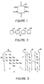
- Figure 1 shows a symbolic diagram of a basic inner product step processor 20.
- This processor performs the inner product step algorithm: where A, B and C are signals.
- the inner product step processor could be visualized as having three storage registers, each register having an input and an output connection.
- the basic unit of time for an array of such inner product step processors would be the time it takes one processor to perform the inner product step of Equation (1).
- the step processor 20 shifts the data on its input lines denoted by A, B and C into the three registers R A , R B and R c ; computes the inner product step where the arrow indicates that the final result is stored in register C; and makes the values stored in R A , R B and R c available on the output lines denoted A, B and C.
- Such an inner product step processor is capable of matrix-vector multiplication when a plurality of them are connected in an array with each inner product step processor coupled to neighboring step processors.
- Figure 2 shows such a processor array 21 where blocks 22, 24, 26 and 28 are all inner product step processors.
- a linear array such as shown in Figure 2 is a convenient organization for matrix-vector operations.
- Matrix-vector multiplication involves multiplication of the data elements of the vector by the rows of a matrix to obtain an output vector. Correlation and convolution, both fundamental operations in signal processing, each can be done by matrix-vector multiplication.
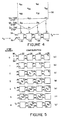
- Figure 3 shows a matrix 30 and vector 32 multiplied to obtain an output vector34.
- the matrix 30 is comprised of a plurality of rows m, and columns n, consisting of individual coefficients. These coefficients can represent the coefficients a lk of polynomial elements, pixel intensities or any one of a number of other possibilities.
- the input vector 32 has the data elements at the time t, while the output vector 34 has the elements at the time t.
- Equation (2) means that the elements of the output vector at time 1 are initially zeroes
- Equation (3) indicates the inner product step operations that are performed in the processor array to determine the subelements of the elements of the output vector.
- y i (k+1) becomes the input signal for the next processor in the array as becomes clear during the discussion of Figures 4 and 5.
- the matrix-vector multiplication represented by Figure 3 can be physically implemented by pipelining the elements x and y of the vectors x and y through w linearly connected processors such as the array shown in Figure 2.
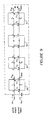
- Figure 4 shows the method of using the linear array of processors of Figure 2 to perform a matrix-vector multiplication such as is shown in Figure 3.
- the general scheme of Figure 4 is to move the elements of the vector y, which are initially zero, to the left on an output line 36 while the elements of the vector x are moving to the right on an input line 38 and the coefficients a lk on the diagonals and offdiagonals in a staggered order of the matrix 30 are moving down into the processors 22, 24, 26 and 28. All moves are synchronized.
- Each element y of the output vector y is able to accumulate all of its subterms before it leaves the network.
- each element y of the output vector y is the summation of the product of each coefficient in the corresponding row i times the corresponding element in the input vector x such that each element y equals the summation of all subelements s 1 with a corresponding coefficient of the row i.
- each element y of the output vector y is the summation of the product of each coefficient in the corresponding row i times the corresponding element in the input vector x such that each element y equals the summation of all subelements s 1 with a corresponding coefficient of the row i.
- Figure 5 shows the configuration of the processor array and positions of the elements of the input and output vectors in the array during each step of the matrix-vector multiplication algorithm shown in Figure 4 embodied by the array of inner product step processors 22, 24, 26 and 28.
- the array of inner product step processors receive the elements x i of the input vector x on the line 38 and the elements of the output vector y leave on the line 36.
- registers in the processors 22, 24, 26 and 28 contain zeroes.
- the register or storage element containing the y vector element will be symbolized by the space in the top part of each processor while the register containing the x vector element will be symbolized by the lower space in the processor.
- the register or storage device containing the coefficient from the matrix 30 is symbolized by the middle section of the box representing each processor.
- FIGS 5(a)-5(g) The time steps of the algorithm are shown in Figures 5(a)-5(g).
- element y is fed into processor 28.
- element x is fed into processor 22 while element y, is moved left one place into the processor 26.
- time step elements x 1 and y 1 continue to move right and left respectively.
- Figure 5(c) or time step 3 shows the coefficient a 11' from the matrix 30, entering the processor 42 where Y 1 is updated so that: where y, is the y, on the line 36 arriving from the processor 26. Thus: after the third time step.
- the coefficients a 12 and a 21 enter the processors 22 and 26 respectively while the x 2 input vector element enters the processor 22 and the y 2 output element enters the processor 26 having entered the processor 28 during the third time step.
- Equation (7) is the complete expression for the element y 1 in the matrix-vector multiplication of Figure 3.
- the first subcomponent or term of y 2 is being generated in the processor 26 as:
- y 3 enters the processor 28 as does the coefficient a 31 and the input signal X 1 so that y 3 becomes:
- the matrix-vector multiplication illustrated in Figures 3-5 involves introducing, at different times, the coefficient on each diagonal of the matrix 30 into one of the processors in the array such that each processor has its multiplication coefficient established as the matrix coefficients on one of the diagonals in the matrix 30.
- the coefficients in the diagonals are arranged into columns in Figure 4 and the elements in the columns are staggered so that as the columns "move" down vertically into the processors, the coefficients arrive in the processors at the proper time, i.e., a 11 arrives in the processor 24 during the third time step, while a 12 and a 21 arrive in the processors 22 and 26 respectively during the fourth time step.
- a fiber optic directional coupler can be used for the processors 22, 24, 26 and 28 where the matrix coefficients establish the coupling between the optical fibers passing through the coupler and the summation occurs optically on the output fiber where the timing of coupling new terms matches the arrival of previously generated terms generated in other couplers.
- the elements of the input vector can be introduced into these couplers on one of the waveguides as light signals with characteristics such as intensity which represent the magnitude of the elements of the input vector.
- the input vector elements x are introduced serially on the input fiber 38. As the elements x progress through the coupler array, they arrive at times coinciding with the arrival times of various coefficients on the diagonals of the matrix. Each such "interception” or simultaneous arrival results in the generation of one term or subelement of one of the elements y of the output vector y.
- Each of these three terms is generated in a different coupler at a different time by the simultaneous arrival of the two operant, e.g., a 21 and x l .
- the term is generated by the coupling of an amount of power from X1 into the output fiber which is equal or proportional to the coefficient a 2 ,. That is, the arrival of the coefficient a 21 in the processor 26 during the fourth time step (step 3, Figure 5(d)) is physically implemented in a fiber optic coupler by tuning the coupler such that it couples a selected amount of the power x into the output fiber.
- the selected amount is related to the magnitude of the coefficient a 21 . In some cases, it will equal a 21 .
- the three terms of y 2 are generated at three different times in three different processors, e.g., time steps 4, 5 and 6 in processors 26, 24 and 22, respectively.
- the intercep- tions representing each term might all occur simultaneously in different processors, or seriatim in the same processor.
- One such alternative embodiment is discussed next.
- separate fibers could be coupled between the input signal source and the coupler array such that each coupler simultaneously received one of the input vector elements and at the same time received one coefficient from a selected row.
- the couplers would couple an amount of power into an output fiber proportional or equal to the matrix coefficient from the row element assigned to that coupler.
- These coupled signals consisting of the terms or subelements of the output vector element corresponding to the selected row, would be summed to provide the selected output vector element. This summation could be done by individual output fibers matched in length and leading to a detector such that all terms or subelements of the output vector element being generated arrive at a single detector simultaneously and are summed therein.
- a single output fiber could be used passing through all the couplers and coupled to a single photodetector.
- the terms of the output vector element which would arrive at different times because of the different distance between each coupler and the detector, could be individually detected and converted to an electrical signal which could be stored in a memory until all the terms were in and then summed with all other terms to arrive at the final value for the output vector element.
- Other elements of optically or electrically summing the terms of each output vector element will be apparent to those skilled in the art.
- a key step in the above-mentioned methods of performing a matrix-vector multiplication involve timing the introduction of the input vector elements and the arrival of the matrix coefficients in the various couplers such that all the terms of the output vector element are generated either simultaneously or seriatim before leaving the array and that multiple processors be used to share the work of generating the terms. That is, the timing of the introduction of the input light signals and the arrival of the matrix coefficients is coordinated such that all the proper input elements intercept all the proper matrix coefficients, either simultaneously or at different times, such that all the terms or subelements of an output vector element are eventually generated by multiple processors in less time than it would take one processor to do all multiplications. The subelements are then optically or electrically summed to derive the final output vector element.
- the array of inner product step processors can compute the w components of y in 2n+w units of time compared to the much larger time that would be needed for a single processor to do the same job.
- a Toeblitz matrix is a matrix which has the property that all the entries on the main diagonal or any off-diagonal, i.e., a line parallel to the main diagonal, are all the same.
- the convolution problem is the matrix-vector multiplication where the matrix is a triangular Toeblitz matrix such as is shown in Figure 6.
- Figure 6 represents the matrix-vector multiplication representing the convolution of the matrix A and of the vector x.
- Figure 7 represents the matrix-vector multiplication representing a four tap filter.
- a discrete Fourier transform can be computed as shown by the matrix-vector multiplication of Figure 8.
- Figure 8 represents the computation to derive the discrete Fourier transform of the vector x.
- processor array and algorithms can be implemented using single mode, fiber optic waveguides and tunable, fiber optic directional couplers. Frequency capabilities well above one gigahertz have been demonstrated in fiber optic recirculating and tapped delay lines. Further, the low dispersion in single mode fiber gives extremely high modulation bandwidths.
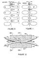
- Figure 9 shows a diagram of a single mode, fiber optic processor array which is comprised of a plurality of fiber optic inner product step processors.
- the array consists of two single mode fiber optic waveguides consisting of an input fiber 45 and an output fiber 46.
- couplers 48-51 are distributed along the length of the fiber.
- Each of the couplers 48-51 has four ports, A-D.
- the input fiber 45 enters the array 52 as the light signal L u p whereupon it enters the port A of the coupler 48 traveling from left to right and exists from the port C of that coupler.
- the input fiber 45 continues through the array from left to right carrying the L up light signal into the A ports and out from the C ports of each of the couplers 48-51 finally leaving the array as the signal R up from the port C of the coupler 51.
- the output fiber 46 is a single mode fiber which enters the array 52 at the port D of the coupler 51 as the signal R down traveling symbolically from right to left. As will be seen above, the light signals, in reality, travel in both fibers in the same direction through each coupler, but the output fiber is coiled so as to feed coupled energy from the input fiber back to the previous coupler for coupling back into the input fiber.
- the output fiber 46 continues through the array entering each coupler at the port D and leaving each coupler at the port B. The output fiber 46 leaves the array from the port B of the coupler 48 as the L down signal.
- the length of the optical fibers between the couplers 48-51 and the number of couplers in the array depends upon the particular application for which the structure is intended.
- the directional couplers 48-51 may be as described by Bergh, Kotler and Shaw in "Single Mode Fiber Optic Directional Coupler", Electronic Letters, Vol. 16, No. 7, March 27, 1980, and U.S. Patent No. 4,493,528 entitled “Fiber Optic Directional Coupler", the details of which are hereby incorporated by reference.
- Such couplers are adjustable such that the amount of light energy coupled between the fibers can be varied from 0% to 100%.
- the couplers 48-51 are linear, symmetric devices whose optical characteristics can be described by the operators t, p, r and T .
- the four above-mentioned operators are defined in terms of the input and output signals from the coupler 48. That is: and Equations (15) and (16) ignore losses in the coupler which are generally 5% or less.
- Equation (15) means that the light power of the light wave at port B at any instant is equal to the light power of the wave entering port A times the tunable coupling operator r 1 plus the light power of the wave entering at port D times the transmission operator T less losses.
- the operator P 1 is equal to r 1 , because the coupler is symmetric.
- the light power of the light wave leaving at port C is equal to the light power entering at port A times the transmission operator t 1 plus the light power entering at the port D times the feedback coupling coefficient P 3.1 less 5% or less losses.
- the operators r 1 and t 1 are related as are T1 and P 1 because of conservation of energy. That is: and Error should be within 5% because of losses in the coupler. Energy entering the coupler is neither created nor destroyed; thus, the same amount of energy that enters each coupler, less some small losses, must leave the coupler.
- the operator t, and ⁇ 1 decrease in proportion to the increase in r and p i .
- the structure of Figure 9 represents the first known fiber optic, systolic array processor. With feedback coupling present, the structure of Figure 9 can also act as a lattice filter within certain limits. That is, a lattice filter is formed by every recirculation loop between two couplers.
- the first coupler 48 couples a selectable amount of energy between the input fiber 45 and the output fiber 46 as determined by the coupling operator r,. It also couples a selectable amount of energy between the output fiber 46 and the input fiber 45 as determined by the coupling operator p i .
- the second coupler 49 does the same thing. That is, part of the energy entering the port A of the coupler 49 in the fiber 45 is coupled into the output fiber 46 by the coupling operator r 2 .
- the operator r 2 is selectable to any amount between 0 and 100%.
- This coupled energy is guided back into the port D of the coupler 48 by the output fiber 46 where a selectable amount of it is coupled back into the input fiber 45 by the first coupler 48.
- the amount of energy fed back into the input fiber 45 is determined by the coupling operator p i which is selectable by the operator.
- This recirculation loop creates a "pole" or peak in the transfer function of the array comprised of the couplers 48 and 49. Since the array is passive, the system will be stable.
- the two coupler array has two outputs, i.e., port C of the coupler 49 and port B of the coupler 48. These two outputs each have a different transfer function relative to the input at port A of the coupler 48.
- a transfer function is the impulse response of the system. That is, an impulse has infinite amplitude and zero width which has an infinite number of Fourier series sinusoidal components of different frequencies and equal magnitude which, when combined, create the impulse signal in the time domain.
- the transfer function defines how the system affects the amplitude and phase of each of the frequency components of the input signal thereby defining the magnitude of that component at the output. When all the output components are combined, an output signal results that may be different than the input signal. Poles are peaks in the transfer function and zeroes are zero or null points in the transfer function.
- the transfer function at the output of the array at the port C of the coupler 49 has only poles, while the transfer function at the output at the port B of the coupler 48 has both poles and zeroes.
- the location of these poles and zeroes in the s plane (or Z plane) of Fourier analysis can be controlled by selection of the coupling operators r and and by selection of the length of the fibers 45 and 46 between the couplers which determines the loop delay T d . Complete specification of any location for any pole or zero is not possible at this time as far as Applicant is aware, but substantial control is possible.
- Equation (15)-(18) the directional couplers 48-51 can be easily used as inner product step processors under certain conditions. If the coupling coefficient is small, r is small and p can be ignored which transforms Equation (15) to: since T is approximately one for small p. Likewise, Equation (16) becomes: for small r and p such that t is approximately one p can be ignored. Equation (19) represents the realization that the linear, symmetrical, fiber optic coupler can function as an inner product step processor for weak backward coupling.
- Equations (19) and (20) are good approximations for small coupling coefficients r and p because, for weak coupling, the signal power on the output fiber 46 in Figure 9 is always about one order of magnitude less than the signal power on the input fiber 45.
- the signal power on the fiber 46 at port B of the coupler 51 is: where R down is initially zero for matrix-vector multiplication as discussed with reference to Figures 3-5. That is, the output vector elements exit on the fiber 46 as the signal L down and R down entering the coupler 51 at the port D is zero.
- the elements of the output vector y are summations of the coupling operators r n set from the matrix coefficients of the matrix 30 times the elements of the input vector x on the fiber 45. Weak coupling therefore results in one order of magnitude difference between the signal power on the fibers 45 and 46.
- Figure 10 shows an embodiment with backward coupling by virtue of the direction of winding of the output fiber 46.
- Figure 11 shows an embodiment with forward coupling by virtue of an opposite direction of winding of the fiber 46 compared to the embodiment of Figure 10.
- the output fibers 46 carry light through the couplers 48-51 in the same direction.
- the direction of winding of the output fiber 46 is such that in Figure 10 the output vector signal leaves the array in the opposite direction from the direction which the output vector leaves the array in Figure 11 such that energy coupled into the output fiber 46 in one coupler is led back to the previous coupler where it is partially or wholly recoupled into the input fiber 45.
- the energy coupled from the input fiber 45 into the output fiber 46 in the coupler 49 returns in the fiber 46 and is coupled back into the input fiber 45 in the coupler 48 in proportion to the coefficient p l .
- the feedback energy travels forward to the coupler 49 and is again coupled into the output fiber 46 in proportion to the coefficient r 2 .
- the energy coupled into the output fiber 46 in each of the couplers 45-51 i.e., the energy is returned to the previous coupler.
- This structure creates feedback coupling which can be advantageously used to create a lattice filter because it provides for poles or peaks in the transfer function which are programmable in location in some extent.
- a lattice filter is more general than a transversal filter in that it offers a transfer function which has both poles and zeroes. In contrast, a transversal filter has only zeroes.
- the physical significance of zeroes in a transfer function is that the zeroes represent frequencies of the input signal which the filter will completely block.
- a transfer function represents the response of a system to an impulse input, i.e., an infinite series of sinusoids of different frequencies and the same amplitude.
- the transfer function is plotted in terms of amplitude of the output versus frequency. That is, the transfer function of the system is the output amplitude and phase of the system at each of the component frequencies of the input waveform.
- a zero in the transfer function means that no output will occur for input frequency components at the frequency of the zero.
- the transfer function is a useful concept because every signal in the time domain can be thought of as a combination of different frequency sinusoids of different amplitudes.
- This series of sinusoids can be applied to any systems and the response of the system to each frequency sinusoid can be computed from the transfer function.
- the output will then consist of a combination of sinusoids having different amplitudes and phases than the corresponding input sinusoids by the action of the system on each frequency component as symbolized by the transfer function.
- These output sinusoids can be combined to derive the output signal in the time domain which results from application of the given input signal to the system.
- the input series of sinusoids is represented by the Fourier transform of the input signal.
- Programmable lattice filters are very desirable because they offer more degrees of freedom for the designer in terms of the number of transfer functions which are available, i.e., the transfer function can be tailored to the specific application.
- a certain class of lattice filters can be implemented.
- a truly general optical lattice filter structure would require completely independent selection of the coefficients t, T , r and p such that any of the four operators which describe the coupler could be any number, positive or negative, and either more or less than one.
- the coefficients t, T , r and p are not independent, but instead are all determined relative to each other once the coupling operator r is established; that is, the coupling operator r establishes p and therefore also establishes t and T by conservation of energy. Further, because the couplers 48-51 are passive, no amplification in the couplers is available. Therefore all the coefficients r, p t, and T are positive and between zero and one. Nevertheless certain lattice filter transfer functions can be implemented with the structure of Figure 10, and adjustments in the transfer function can be made.
- the scattering and recirculation effects in the loops 55-57 and 59-61 allow the system of Figure 10 to also be used to model physical phenomena described by the Redheffer scattering formalism.
- a physical system such as light passing through a series of plane, two-way, partially reflecting and partially transmitting mirrors is described by this Redheffer formalism and is analogous to the feedback of the embodiment of Figure 10.
- the embodiment of Figure 11 can be used as a transversal filter.
- Transversal filters are well known in the art, and optical tapped delay lines have been used to implement them.
- H. F. Taylor described a fiber optic transversal filter in "Fiber and Integrated Optical Devices For Signal Processing", published in SPIE, Vol. 176, Guided Wave Optical Systems & Devices (1979) at page 17.
- transversal filters are used in signal processing applications to implement narrow band filters and matched filters.
- the Taylor tapped delay line transversal filter uses individual modulators on fibers of different lengths and combines the optical outputs in a single photodetector.
- the individual modulators vary the tap weights and the individual fiber lengths determine the delay between taps and determines the tap spacing.
- Taylor's filter requires a single photodetector which would be optically coupled to the ends of all the individual fibers in the bundle, which detector would, of necessity, be of large physical dimensions.
- a transversal filter utilizing the embodiment of the embodiments of Figure 11 would not need such a large photodetector, which is a significant advantage since small photodetectors can operate faster, i.e., at higher frequencies than large photodetectors.
- the zeros in the transfer function can be moved to change the band stop frequency characteristics of the filter by changing the tuning of the couplers. Further, the length of fiber between the couplers can be changed to alter the transfer function somewhat. Such programmability of the transfer function gives the designer greater flexibility in his designs and can open new avenues for uses not before possible.
- the couplers of the present invention include two strands 45 and 46 of a single mode fiber optic material mounted in longitudinal arcuate grooves 63A and 63B, respectively, formed in flat, confronting surfaces 64A and 64B, respectively, of rectangular bases or blocks 66A and 66B.
- the block 66A with the strand 45 mounted in the groove 63A will be referred to as the coupler half 70A
- the block 66B with the strand 46 mounted in the groove 63B will be referred to as the coupler half 70B.
- Each of the strands 45 and 46 comprises a commercially available fiber of quartz glass which is doped to have a central core and an outer cladding. It will be seen below that the present invention is particularly advantageous for use with single mode fibers, which typically have a core diameter on the order of 10 microns or less and a cladding diameter on the order of 125 microns. However, the invention may also be employed with other types of fibers, such as multimode fibers. In the embodiment disclosed, single mode fibers are utilized; however, for clarity of illustration, the diameter of the strands 45 and 46 and their respective cores are exaggerated. Furthermore, test results described herein are for couplers utilizing single mode fibers.
- the arcuate grooves 63A and 63B have a radius of curvature which is very large compared to the diameter of the fibers 45 and 46 and have a width slightly larger than the fiber diameter to permit the fibers 45 and 46, when mounted therein, to conform to a path defined by the bottom walls of the grooves 63.
- the depth of the grooves 63A and 63B varies from a minimum at the center of the blocks 66A and 66B, respectively, to a maximum at the edges of the blocks 66A and 66B, respectively.
- the grooves 63 are illustrated as being rectangular in cross section; however, it will be understood that other suitable cross-sectional contours which will accommodate the fibers may be used alternatively, such as a U-shaped cross section or a V-shaped cross section.
- the depth of the grooves 63 which mount the strands 45 and 46 is less than the diameter of the strands, while at the edges of the blocks 66, the depth of the grooves is preferably at least as great as the diameter of the strands.
- Fiber optic material is removed from each of the strands 45 and 46 as shown at 78b in Figure 15 to form the respective, identical, oval-shaped planar surfaces 78A, 78B, which are coplanar with the confronting surfaces 64A, 64B, respectively. These surfaces 78A, 78B will be referred to herein as the fiber "facing surfaces".
- the amount of fiber optic material removed increases gradually from zero towards the edges of the block 66 to a maximum towards the center of the block. This tapered removal of the fiber optic material enables the fibers to converge and diverge gradually, which is advantageous for avoiding backward reflection and excess loss of light energy.
- the coupler halves 70A and 70B are identical, and are assembled by placing the confronting surfaces 64A and 64B of the blocks 66A and 66B together, so that the surfaces 78A and 78B of the strands 45 and 46 are in facing relationship.
- index matching substance such as index matching oil, is provided between the confronting surfaces 64.
- This substance has a refractive index approximately equal to the refractive index of the cladding, and also functions to prevent the optically flat surfaces 64 from becoming permanently locked together.
- the oil is introduced between the blocks 66 by capillary action.
- An interaction region 72 is formed at the junction of the strands 45 and 46, in which light is transferred between the strands by evanescent field coupling. It has been found that, to ensure proper evanescent field coupling, the amount of material removed from the fibers must be carefully controlled so that the spacing between the core portions of the strands 45 and 46 is within a predetermined "critical zone".
- the evanescent fields extend into the cladding and decrease rapidly with distance outside their respective cores. Thus, sufficient material should be removed to permit each core to the positioned substantially within the evanescent field of the other. If too little material is removed, the cores will not be sufficiently close to permit the evanescent fields to cause the desired interaction of the guided modes, and thus, insufficient coupling will result.
- each strand receives a significant portion of the evanescent field energy from the other strand, and optimum coupling is achieved without significant energy loss.
- the critical zone is illustrated schematically in Figure 16 as including that area, designated by the reference numeral 73, in which the evanescent fields, designated by reference numerals 74A and 74B, of the fibers 45 and 46, respectively, overlap with sufficient strength to provide coupling, i.e., each core is within the evanescent field created by the light traveling in the other core.
- mode perturbation occurs within the area 73 when the cores are brought too close together.
- the critical zone is defined as that area in which the evanescent fields 74 overlap with sufficient strength to cause coupling without substantial mode perturbation induced power loss.
- the critical zone for a particular coupler is dependent upon a number of interrelated factors such as the parameters of the fiber itself and the geometry of the coupler. Further, for a single mode fiber having a step-index profile, the critical zone can be quite narrow. In a single mode fiber coupler of the type shown in Figures 12-15, for example, the required center-to-center spacing between the strands 45 and 46 at the center of the coupler as shown in Figure 14 is typically less than a few (e.g., 2-3) core diameters.
- the strands are (1) identical to each other, (2) have the same radius of curvature at the interaction region 32, and (3) have an equal amount of fiber optic material removed therefrom to form their respective facing surfaces 78A and 78B.
- the fibers 45 and 46 are symmetrical, through the interaction region 72, in the plane of the facing surfaces 78, so that the facing surfaces 78 are coextensive if superimposed. This ensures that the two fibers 45 and 46 will have the same propagation characteristics at the interaction region 72, and thereby avoids coupling attenuation associated with dissimilar propagation characteristics.
- the blocks or bases 66A and 66B may be fabricated of any suitable rigid material.
- the bases comprise generally rectangular blocks of fused quartz glass approximately one inch long, one inch wide, and 0.4 inch thick.
- the fiber optic strands 45 and 46 are secured in the slots 63 by suitable cement 79, such as epoxy glue.
- suitable cement 79 such as epoxy glue.
- One advantage of the fused quartz blocks 66 is that they have a coefficient of thermal expansion similar to that of glass fibers, and this advantage is particularly important if the blocks 66 and fibers 45 and 46 are subjected to any heat treatment during the manufacturing process.
- Another suitable material for the block 66 is silicon, which also has excellent thermal properties for this application.
- the coupler includes four ports labeled A, B, C, and D, in Figure 12.
- ports A and D which correspond to strands 45 and 46, respectively, are on the lefthand side of the coupler, while the ports B and C, which correspond to the strands 45 and 46, respectively, are on the righthand side of the coupler.
- input light is applied to port A. This light passes through the coupler and is output at port C and/or port B, depending upon the amount of power that is coupled between the strands 45 and 46.
- the term "normalized coupled power" is defined as the ratio of the coupled power to the total output power.
- the normalized coupled power would be equal to the ratio of the power at port B to the sum of the power output at ports B and C. This ratio is also referred to as the "coupling efficiency" and when so used is typically expressed as a percent.
- the term "normalized coupled power” it should be understood that the corresponding coupling efficiency is equal to the normalized coupled power times 100.
- the coupler of the type shown in Figure 12 has a coupling efficiency of up to 100%.
- the coupler may be "tuned" to adjust the coupling efficiency to any desired value between zero and the maximum of 100% power coupling, by offsetting the facing surfaces of the blocks 16A and 16B.
- Tuning the coupler changes the coupling efficiency and changes the coupling and transmission operators r, p, T and t. That is, when the coupling efficiency is lowered, less power is coupled from part A to part B in Figure 12. That means that 5 and p are decreased because the coupler is symmetric and that t and T are increased since less energy leaving either fiber for the other means more energy remains in the original fiber and is transmitted through the coupler by conservation of energy.
- Such tuning is preferably accomplished by sliding the blocks 66A and 66B laterally relative to each other in the direction of the arrow in Figure 14.
- the coupler is sensitive to displacements of the fibers in a direction which laterally offsets the planar faces such as the direction of the arrow in Figure 14.
- the coupler is less sensitive to displacements which longitudinally offset the planar faces, i.e., in a direction perpendicular to the arrow in Figure 14 and coming out of the page in orthogonal fashion.
- the coupler is relatively insensitive to displacement of the fibers which rotationally offsets the faces. The sensitivity of the coupling operators to displacement of the fibers depends upon the spacing of the cores of the fibers when the fibers are superimposed.
- the coupler is highly directional, with substantially all of the power applied at one side of the coupler being delivered to the other side of the coupler. That is, substantially all of the light applied to input port A is delivered to the output ports B and C, without contradirectional coupling to port D. Likewise, substantially all of the light applied to input port D is delivered to the output ports B and C. Further, this directivity is symmetrical. Thus, light supplied to either input port C or input port B is delivered to the output ports D or A, respectively, and light supplied to either port A or port D is defined either to the port B or C respectively.
- the coupler is essentially nondiscriminatory with respect to light polarizations, and preserves the polarization of the coupled light during the power transfer. Thus, for example, if a light beam having a vertical polarization is input to port A, the light coupled from port A to port B as well as the light passing straight through from port A to port C will remain vertically polarized.
- FIG 17-19 there is shown the construction for a fiber optic tapped delay line which could be used to implement the arrays depicted in Figures 10 and 11.
- Two of the constructions shown in Figure 17 optically coupled together at the taps could implement the arrays of Figures 10 and 11 as will be apparent from the following discussion.
- a single element of optical fiber 45 is used, beginning at an input end 80 which is supplied with a light input signal from a light source 82, and ending at an output end 84.
- the optical fiber 45 is wound around a chip 86 with V-grooves 90a-90y formed therein.
- the chip 86 is a thin slice of silicon with grooves 90a-90y photolithographically etched therein and will be described in more detail later.
- the first portion of the fiber on the chip is designated the first winding 86a
- the second portion of the fiber 45 mounted on the chip 86 is designated 86b, and so on.
- taps are constructed so that each revolution of the optical fiber 45 is tapped at the lateral line 88.
- the construction of the chip 86 and the V-grooves and the manner by which the optical fiber 45 is laid in the V-grooves in the chip 86 is described in more detail in U.S. Patent No. 4,558,920, entitled "Tapped Optical Fiber Delay Line". Standard photolithographic etching techniques known in the semiconductor industry can be used to form the V-grooves in the chip 86.
- V-grooves there is a need for great precision in the construction of the V-grooves such that they all are identical in width and depth since the fiber segments of the fiber 45 in the grooves must be coplanar. Any technique which will not meet the criterion can be used such as by laser or other chemical or mechanical machining. It has been found it is satisfactory to use 100 oriented silicon for the chip 86 with chemical etching by photolithographic techniques as is well known in the semiconductor manufacturing art. Silicon of the 100 orientation yields a V-groove with walls at an angle of 54.74 degrees.
- the first step in forming the V-grooves is photolithographically etching flat grooves with the width of the flat grooves determined by the depth needed of the V-groove.
- the depth of the V-groove needed depends upon the size of the fiber being used.
- the preferred way to construct an optical tap is to have the optical fiber surface mounted in a curved configuration so that a flat portion of the optical fiber may be lapped to form a planar face to provide a tap of the light traveling within the fiber.
- the silicon chip 86 is mounted on a block of quartz 87 which has a curved upper surface. It has been found that a silicon chip of standard thickness (0.25 millimeter) and about three-centimeter length can be bent without breaking around a twelve-inch radius. An adhesive substance such as wax is used to hold the silicon chip 86 on the quartz block 87 in the curved configuration shown in Figure 17.
- the optical fiber 45 may now be mounted on silicon chip 85.
- the portions of the optical fiber 45 which are to be mounted in the V-grooves preferably have the protective jacket removed.
- ITT type monomode fiber has a plastic jacket which may be removed by dipping it in sulfuric acid. The resiliency of the plastic jacket prevents precision in the lapping operation, so it should be removed.
- Corning type fiber has a lacquer jacket which may be removed by dipping it in acetone. Since the lacquer jacket is more solid than the plastic jacket, its removal is preferential rather than mandatory.
- FIG 18 shows a cross-sectional view along the line 18-18 in Figure 17.
- Figure 19 shows a cross-section of the first three grooves in more detail.
- a portion of the optical fiber 86a near the input end 80 of the fiber is mounted in the second V-groove 90a of the silicon chip 85.
- there is a first V-groove 90x which is not used to receive the optical fiber 45, but rather is used for alignment purposes.
- an adhesive substance 92 is placed in the bottom of the V-groove 90a. Therefore, when the portion 86a of the optical fiber 45 is placed in the V-groove 90a and the optical fiber 45 bottoms out against the sides of the V-groove 90a, it will be permanently retained there by the adhesive 92.
- a length L of the optical fiber is left between the center of the fiber portion 86a and the center of the second fiber portion 86b of the optical fiber 45, which is to be mounted in the second V-groove 86b.
- This length L is the length of optical fiber shown as one of the fibers forming the loop offiber45 in Figure 17. It provides a delay time equal to the period of the desired fundamental frequency of the transversal filter or the desired loop delay for the matrix-vector multiplier to be constructed using the structure of Figure 17.
- the optical fiber 45 is wound around the silicon chip 86 so that upon each successive revolution it is fitted into the next succeeding V-groove and secured there bythe adhesive 92.
- the optical fiber 45 terminates at the end 84 as shown in Figure 17.
- the next step is to mechanically lap the upper surface of the portions 86 of the optical fiber 45 at the lateral line 88.
- the portions 86 of the optical fiber45 being mechanically mounted in the silicon chip by the adhesive 92, are stable enough to have portions of the cladding removed by lapping.
- This lapping operation will remove a portion of the cladding 92 to form a planarface similarto the face 78b, shown in Figure 15. It is importantto note that not all of the cladding material 92 (92a-c in Figure 19) around the core 94 (94a-c in Figure 19) of the optical fiber is to be removed.
- each core 94 and the lapped surface 96 of the fiber segments 86 in the V-grooves depends on the amount of light which is to be removed from the fiber at each tap.
- the lapped surface 96 should be further from the core 94 of the fiber segments 86. Since it is desirable to have a high number of taps for certain applications, only a small amount of light can be removed at each tap. Therefore, between approximately five and ten microns of cladding will be left between the lapped surface 96 and the core 94 of each of the fiber segments 86.
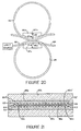
- Figure 20 shows the combined structure representing the structure of either Figure 10 or Figure 11 with the number of couplers equal to the number of turns of the fibers 45 and 46 in the V-grooves. Whether the structure of Figure 20 represents the structure of Figure 10 or Figure 11 depends upon the direction of the winding of the fiber 46.
- the fiber 46 is wound so as to carry the coupled light back to the next preceding tap, i.e., in the direction from which the light in the input fiber 45 came, then feedback or backward coupling is present and the structure can function as a lattice filter. If the winding direction is opposite, a transversal or matched filter will be implemented.
- Figure 21 shows a cross-section of the structure of Figure 20 taken along the view line 22-22 in Figure 20 corresponding to the line 88 in Figures 17 and 20.
- the structure is simply two chips 86a and 86b with V-grooves therein and supported by curved quartz blocks 87a and 87b affixed together such that the V-grooves 90a-90n in the chip 86a are in predetermined alignment with the V-grooves 90a'-90n' in the chip 85b.
- Alignment grooves 100 and 100' and 102 and 102' at the opposite ends of the chips 86a and 86b contain alignment beads 104 and 106.
- each of the V-grooves 90a-90n and 90a'-90n' establish fixed reference points from which each of the V-grooves 90a-90n and 90a'-90n' can be precisely located. If it is desired that each coupler formed by a pair of V-grooves have the same coupling operators rand p as each of the other couplers, then each pair of grooves forming a coupler should be located the same distance from the alignment grooves plus a selected differential offset of one groove in the pair relative to the other groove so that each fiber pair has the same relative offset as each other pair. In some applications of lattice ortransversal filtering this equal weighting of taps will be desirable.
- couplers with unequal coupling at each tap using the structure of Figures 20 and 21.
- the relative offsets of each of the fiber pairs in the opposing grooves can be established by varying the distance of one of the opposing grooves from the alignment groove versus the distance to the alignment grooveforthe opposite V-groove. Since the photolithographic operation described above can be controlled to within reasonable tolerances, such a method of offsetting the V-grooves can give filters with weighted taps.
- Figures 20 and 21 can also be used to perform matrix-vector multiplication operations.
- the advantage of the structure of Figures 20 and 21, as will become apparent from the discussion below, is that very large matrices with many coefficients can be handled in a very fast systolic array using pipeline concepts.
- FIG 22 there is shown a 2x2 Toeblitz matrix 100, multiplied by an input vector x 112, to give an output vector y 114.
- Figures 22-24 will be used to illustrate how the arrays of Figures 10,11 or 20 may be used to perform matrix-vector multiplication on Toeblitz matrices. If the matrix 110 is a Toeblitz matrix, the coefficients a 11 and a 22 will be equal because they are on the same diagonal.
- the elements y, and y 2 of the output vector are equal to: and
- Figure 23 represents the array of fiber optic couplers which can be used to perform the matrix-vector multiplication of Figure 22.
- each of the couplers 114-116 can be described by transmission and coupling operators r, t, p and T . Therefore, each of the couplers 114-116 can be approximately characterized in terms of its input and output light signals L up, R up , L down and R down and the operators t, r, p and T per equations (15) and (16). Since weak coupling operators r and p are assumed for matrix-vector multiplication, only the transmission and coupling operators t, r and T are considered since, as described above, the effects of p on the input optical fiber 45 are negligible for weak coupling.
- each of the couplers 114-116 operates as an inner product step processor and each is characterized by the equations (19) and (20).
- the coupler 114 is tuned so that its coupling operator r 1 equals the matrix coefficient a, 2 .
- the coupler 115 has its coupling operator r 2 tuned to the matrix coefficients a 11 and a 22
- the coupler 116 has its coupling operator r 3 tuned to the matrix coefficient a, 2 , a 2 ,.
- FIGS 24(A)-(D) The operation of the couplers 114-116 in performing the matrix-vector multiplication is illustrated in Figures 24(A)-(D).
- the operation begins, as shown in Figure 24(A), with the serial introduction into the input optical fiber 45 of the two light signals which represent the elements of the input vector x, i.e., the signals X 1 and x 2 .
- Time is increasing to the right of all of Figures 24(A)-(D). Therefore, the signal X 1 arrives at the coupler 114 on the fiber 45 earlier than the signal x 2 .
- the signals X 1 and X 2 are traveling in the fiber 45 from left to right in Figure 23.
- This signal a 12 x 1 leaves the coupler 114 first in time.
- the signals in Figure 24(B) can be thought of as emerging from the coupler 114 moving from right to left on the output fiber 46 with the signal a 12 x 1 emerging first.
- the output signals pass through the couplers in the same direction as the input signals.
- the signals a 11 x 1 and a 21 x 1 are coupled into the output fiber 46 as the signal x 1 passes through the couplers 115 and 116, respectively.
- Figure 24(C) shows the signals that are generated in the output fiber 46 as the input signal x 2 passes through the couplers 114-116. These signals must be summed with the signals generated from the input signal x 1 because of equations (22) and (23) above. Thus, the signal a 12 x 2 must be coupled into the output fiber 46 just as the signal a 11 x 1 is arriving at the coupler 114. The time spacing of introduction of the input signals x 1 and x 2 must therefore be equal to the round trip propagation time T d of a light pulse from one coupler to the next coupler and back to the preceding coupler.
- the signals a 11 x 1 and a 12 x 2 are optically summed in the output fiber 46 as are the signals a 21 x 1 and a 22 x 2 .
- Figure 24(D) shows the resulting output on the output fiber 46. Since only the middle two pulses y, and y 2 define and output vector y, the pulses a 12 x 1 and a 21 x 2 are discarded. This can be done electronically by selecting from the output of a detector only the signals during the time window shown in Figure 24(D). This can be done in any conventional manner. The structure used to do it is not critical to the invention but one way to do it would be to establish the time base and spacing of the input pulses with a counter. The time window would then correspond to a series of numbers in the count. Two decoders could be coupled to the output of the counter to determine when the first number in the series marking the time t 1 occurred.
- This decoder would turn on or open the gate on the output of the detector at time t i .
- the second decoder coupled to the output of the counter, would determine when the count corresponding to t 2 occurred and turn off or close the gate on the output of the detector at that time.
- a pulse generator 118 generates an electrical pulse. This pulse is split into the number of elements in the input vector by a splitter means represented by the splitter 120.
- the splitter 120 in Figure 25 can be any conventional design.
- the two pulses from the splitter 120 are coupled into the inputs of conventional attenuators 122 and 124 which serve to attenuate the two pulses to the levels of the pulses X1 and x 2 .
- a delay line 128 serves to delay the pulse x 2 for the period T d to achieve the proper pulse spacing.
- a conventional mixer 130 then recombines the pulses on the conductors 132 and 134 onto the conductor 126 where they are coupled to the input of a laser diode 136. There they are converted to light pulses on the fiber 45.
- the fiber 45 then passes through the couplers 114-116 which couple varying amounts of power into the output fiber 46 as previously described regarding Figures 22-24.
- the output fiber 46 is coupled to the input of a photodetector 138 which reconverts the pulses to electrical pulses on the line 140.
- the pulses are amplified in an amplifier 142 and coupled to the input of an oscilloscope 144 where they are displayed.
- the embodiment of Figure 25 does not use a time window gating circuit, depending instead upon manual selection and measurement of the middle two pulses on the scope display.
- Figure 26 illustrates a matrix-vector multiplication example which was actually used with the physical system depicted in Figure 25 to verify the correct operation of the system.
- Figure 27 illustrates the light pulses actually observed at the input to the system of Figure 25 and the light pulses actually observed at the output.
- the input pulses X1 and x 2 are equal because both elements of the input vector x and 1 in Figure 26.
- Figures 28 and 29 which show the same things as Figures 26 and 27 except for a different set of coefficients in the matrix and a different input vector.
- any NxN size Toeblitz matrix can be handled with the arrays of Figures 10 and 20. It is only necessary to have 2N-1 couplers corresponding to the 2N-1 main and off-diagonals of the matrix. The components of the input vector enter the couplers progressively in such a way that each coupler sees matrix elements from a single main or off-diagonal. In the future when couplers become available where the coupling and transmission operators can be rapidly changed, it will be possible to handle the general, non-Toeblitz matrix. Until then, only Toeblitz matrices can be handled if the high inherent bandwidth of the fiber optic processor array is to be fully utilized. In the general NxN Toeblitz matrix case, the N components of the output vector will appear on the output fiber 46 following the (N-1) th output pulse.
- the 2N-1 couplers can be properly adjusted to yield an impulse response, i.e., an overall transfer function, which gives pulse heights in the output vector proportional to a 1,N , a 2 , N - 1 , ..., a i,N -i+1'... a N.1 respectively.
- the weak coupling requirement can be removed. That is, the weak coupling requirement can possibly be removed if the couplers can be adjusted to properly account for the resulting recirculations and give the correct overall transfer function to get a correct output vector.
- a major advantage of the processor array described herein is the single fiber nature of the output. This enables the use of a very small and, therefore, very fast detector without sacrificing light collection efficiency.
- the factors that determine the ultimate accuracy of the multiplier are the settings of the couplers to program the impulse response, the time delay between the input pulses, the loop delays, and the residual recirculation and frequency bandwidth of the electronic components. With smaller components and a closely packed geometry, the delays can be reduced to the order of 0.1 ns allowing a 10 GHz data rate. Similar or higher rates could be obtained if the systolic array were implemented using integrated optics techniques.
- the fiber optic signal processor arrays of Figure 10 and 20 can serve as feedback lattice filter with an infinite impulse response as opposed to the finite impulse response of the tapped delay line and a programmable transfer function.
- This lattice type filter has the advantage that it has both poles and zeroes compared to only zeroes in tapped delay line transversal filters. This offers more flexibility to a designer that needs a transfer function with poles in it. The order of the system, i.e., the number of poles, depends upon the number of loops between couplers.
- a dual feed forward lattice filter can also be implemented by replacing the scattering couplers by forward couplers which operate on Lu p and L down to produce R u p and R d own. The ability of this last forward transfer structure to perform matched filtering has already been analyzed and demonstrated using multimode fibers on non-tunable couples by E. Marom, supra.
Landscapes
- Engineering & Computer Science (AREA)
- Physics & Mathematics (AREA)
- Theoretical Computer Science (AREA)
- General Physics & Mathematics (AREA)
- Mathematical Physics (AREA)
- Optics & Photonics (AREA)
- Software Systems (AREA)
- Nonlinear Science (AREA)
- Data Mining & Analysis (AREA)
- Databases & Information Systems (AREA)
- Signal Processing (AREA)
- General Engineering & Computer Science (AREA)
- Optical Communication System (AREA)
- Complex Calculations (AREA)
- Image Processing (AREA)
- Optical Integrated Circuits (AREA)
- Electrophonic Musical Instruments (AREA)
- Gyroscopes (AREA)
- Optical Fibers, Optical Fiber Cores, And Optical Fiber Bundles (AREA)
- Laser Surgery Devices (AREA)
- Compression, Expansion, Code Conversion, And Decoders (AREA)
- Light Guides In General And Applications Therefor (AREA)
Claims (25)
Priority Applications (1)
| Application Number | Priority Date | Filing Date | Title |
|---|---|---|---|
| AT83303550T ATE52861T1 (de) | 1982-06-21 | 1983-06-20 | Signalprozessor fuer optisch geleitete wellen zur matrixvektor-multiplikation und filterung. |
Applications Claiming Priority (2)
| Application Number | Priority Date | Filing Date | Title |
|---|---|---|---|
| US39066482A | 1982-06-21 | 1982-06-21 | |
| US390664 | 1982-06-21 |
Publications (3)
| Publication Number | Publication Date |
|---|---|
| EP0099193A2 EP0099193A2 (fr) | 1984-01-25 |
| EP0099193A3 EP0099193A3 (en) | 1986-08-20 |
| EP0099193B1 true EP0099193B1 (fr) | 1990-05-16 |
Family
ID=23543421
Family Applications (1)
| Application Number | Title | Priority Date | Filing Date |
|---|---|---|---|
| EP83303550A Expired - Lifetime EP0099193B1 (fr) | 1982-06-21 | 1983-06-20 | Processeur de signaux d'ondes optiques guidées pour multiplication matrice-vecteur et pour filtrage |
Country Status (10)
| Country | Link |
|---|---|
| EP (1) | EP0099193B1 (fr) |
| JP (1) | JPS5990816A (fr) |
| KR (1) | KR910005324B1 (fr) |
| AT (1) | ATE52861T1 (fr) |
| AU (1) | AU571442B2 (fr) |
| BR (1) | BR8303264A (fr) |
| CA (1) | CA1213063A (fr) |
| DE (1) | DE3381571D1 (fr) |
| IL (1) | IL69003A (fr) |
| NO (1) | NO832228L (fr) |
Families Citing this family (6)
| Publication number | Priority date | Publication date | Assignee | Title |
|---|---|---|---|---|
| GB2154772B (en) * | 1984-02-25 | 1987-04-15 | Standard Telephones Cables Ltd | Optical computation |
| GB2233109B (en) * | 1989-06-13 | 1993-05-12 | Plessey Co Plc | Optical fibre lattice signal processors |
| EP0629896B1 (fr) * | 1993-06-21 | 2001-10-17 | Nippon Telegraph And Telephone Corporation | Processeur de signaux optiques, méthode pour son contrôle, méthode pour sa conception et méthode pour sa fabrication |
| US5596661A (en) * | 1994-12-28 | 1997-01-21 | Lucent Technologies Inc. | Monolithic optical waveguide filters based on Fourier expansion |
| JP7310906B2 (ja) * | 2019-10-02 | 2023-07-19 | 日本電信電話株式会社 | 光分岐回路作製方法及び光分岐回路作製装置 |
| CN115826144A (zh) * | 2022-10-31 | 2023-03-21 | 中国航天三江集团有限公司 | 一种全光纤高阶模滤波器及其制造方法 |
Family Cites Families (4)
| Publication number | Priority date | Publication date | Assignee | Title |
|---|---|---|---|---|
| JPS579041B2 (fr) * | 1974-11-29 | 1982-02-19 | ||
| US4493528A (en) * | 1980-04-11 | 1985-01-15 | Board Of Trustees Of The Leland Stanford Junior University | Fiber optic directional coupler |
| AU6578281A (en) * | 1980-12-16 | 1981-07-22 | Commw Scient Ind Res Org | Signal processing apparatus and method |
| US4558920A (en) * | 1981-11-19 | 1985-12-17 | Board Of Trustees Of The Leland Stanford Junior University | Tapped optical fiber delay line |
-
1983
- 1983-06-15 IL IL69003A patent/IL69003A/xx unknown
- 1983-06-20 AU AU15946/83A patent/AU571442B2/en not_active Expired - Fee Related
- 1983-06-20 EP EP83303550A patent/EP0099193B1/fr not_active Expired - Lifetime
- 1983-06-20 DE DE8383303550T patent/DE3381571D1/de not_active Expired - Lifetime
- 1983-06-20 CA CA000430741A patent/CA1213063A/fr not_active Expired
- 1983-06-20 NO NO832228A patent/NO832228L/no unknown
- 1983-06-20 JP JP58111789A patent/JPS5990816A/ja active Pending
- 1983-06-20 AT AT83303550T patent/ATE52861T1/de not_active IP Right Cessation
- 1983-06-20 KR KR1019830002751A patent/KR910005324B1/ko not_active Expired
- 1983-06-30 BR BR8303264A patent/BR8303264A/pt unknown
Also Published As
| Publication number | Publication date |
|---|---|
| ATE52861T1 (de) | 1990-06-15 |
| EP0099193A3 (en) | 1986-08-20 |
| CA1213063A (fr) | 1986-10-21 |
| DE3381571D1 (de) | 1990-06-21 |
| BR8303264A (pt) | 1984-02-07 |
| AU1594683A (en) | 1984-01-05 |
| KR840005236A (ko) | 1984-11-05 |
| EP0099193A2 (fr) | 1984-01-25 |
| AU571442B2 (en) | 1988-04-21 |
| IL69003A (en) | 1987-12-31 |
| NO832228L (no) | 1983-12-22 |
| JPS5990816A (ja) | 1984-05-25 |
| IL69003A0 (en) | 1983-10-31 |
| KR910005324B1 (ko) | 1991-07-25 |
Similar Documents
| Publication | Publication Date | Title |
|---|---|---|
| US4588255A (en) | Optical guided wave signal processor for matrix-vector multiplication and filtering | |
| KR930001532B1 (ko) | 캐스케이드식 광학 섬유 격자휠터 | |
| US4723827A (en) | Fiber optic switch and discretely variable delay line | |
| US4511207A (en) | Fiber optic data distributor | |
| EP0340987B1 (fr) | N x N coupleur optique en étoile | |
| EP0080841B1 (fr) | Double couplage à fibre-optique et mémoire de recirculation | |
| US4934777A (en) | Cascaded recirculating transmission line without bending loss limitations | |
| US6735368B2 (en) | Optical delay device | |
| US4558920A (en) | Tapped optical fiber delay line | |
| EP0563068B1 (fr) | Dispositif de division de l'intensite | |
| EP0430516B1 (fr) | Réseau périodique avec un diagramme de rayonnement d'élément quasi-idéal | |
| EP0450747B1 (fr) | Coupleur optique intégré | |
| WO1992011555A1 (fr) | Dispositif optique | |
| US4515428A (en) | Integrated optical star coupler | |
| US4676585A (en) | Continuously variable fiber optic delay line | |
| GB2163919A (en) | Optical demultiplex transmission equipment | |
| EP0099193A2 (fr) | Processeur de signaux d'ondes optiques guidées pour multiplication matrice-vecteur et pour filtrage | |
| Thurston et al. | Analysis of mode separation in multichannel branching waveguides | |
| US4598975A (en) | Multiple fiber linear array and method of making same | |
| US4402568A (en) | Method and apparatus for an optical four-gate coupler | |
| CA1231566A (fr) | Processeur de muliplication matricielle-vectorielle et de filtrage pour signaux lumneux guides | |
| EP0106505B1 (fr) | Générateur de mot à fibre optique | |
| JPS6138907A (ja) | フアイバ光学フイルタ | |
| GOTO et al. | Optical signal processor using collinear acousto-optic interaction with applications to matrix multiplication | |
| US7260291B2 (en) | Coupled mode arrayed waveguide grating |
Legal Events
| Date | Code | Title | Description |
|---|---|---|---|
| PUAI | Public reference made under article 153(3) epc to a published international application that has entered the european phase |
Free format text: ORIGINAL CODE: 0009012 |
|
| AK | Designated contracting states |
Designated state(s): AT BE CH DE FR GB IT LI LU NL SE |
|
| PUAL | Search report despatched |
Free format text: ORIGINAL CODE: 0009013 |
|
| AK | Designated contracting states |
Kind code of ref document: A3 Designated state(s): AT BE CH DE FR GB IT LI LU NL SE |
|
| 17P | Request for examination filed |
Effective date: 19870210 |
|
| 17Q | First examination report despatched |
Effective date: 19880129 |
|
| GRAA | (expected) grant |
Free format text: ORIGINAL CODE: 0009210 |
|
| AK | Designated contracting states |
Kind code of ref document: B1 Designated state(s): AT BE CH DE FR GB IT LI LU NL SE |
|
| PG25 | Lapsed in a contracting state [announced via postgrant information from national office to epo] |
Ref country code: SE Effective date: 19900516 Ref country code: NL Effective date: 19900516 Ref country code: LI Effective date: 19900516 Ref country code: CH Effective date: 19900516 Ref country code: BE Effective date: 19900516 Ref country code: AT Effective date: 19900516 |
|
| REF | Corresponds to: |
Ref document number: 52861 Country of ref document: AT Date of ref document: 19900615 Kind code of ref document: T |
|
| ITF | It: translation for a ep patent filed | ||
| REF | Corresponds to: |
Ref document number: 3381571 Country of ref document: DE Date of ref document: 19900621 |
|
| ITTA | It: last paid annual fee | ||
| PG25 | Lapsed in a contracting state [announced via postgrant information from national office to epo] |
Ref country code: LU Free format text: LAPSE BECAUSE OF NON-PAYMENT OF DUE FEES Effective date: 19900630 |
|
| ET | Fr: translation filed | ||
| REG | Reference to a national code |
Ref country code: CH Ref legal event code: PL |
|
| NLV1 | Nl: lapsed or annulled due to failure to fulfill the requirements of art. 29p and 29m of the patents act | ||
| PLBE | No opposition filed within time limit |
Free format text: ORIGINAL CODE: 0009261 |
|
| STAA | Information on the status of an ep patent application or granted ep patent |
Free format text: STATUS: NO OPPOSITION FILED WITHIN TIME LIMIT |
|
| 26N | No opposition filed | ||
| PGFP | Annual fee paid to national office [announced via postgrant information from national office to epo] |
Ref country code: FR Payment date: 19910614 Year of fee payment: 9 Ref country code: DE Payment date: 19910614 Year of fee payment: 9 |
|
| PGFP | Annual fee paid to national office [announced via postgrant information from national office to epo] |
Ref country code: GB Payment date: 19910628 Year of fee payment: 9 |
|
| PG25 | Lapsed in a contracting state [announced via postgrant information from national office to epo] |
Ref country code: GB Effective date: 19920620 |
|
| GBPC | Gb: european patent ceased through non-payment of renewal fee |
Effective date: 19920620 |
|
| PG25 | Lapsed in a contracting state [announced via postgrant information from national office to epo] |
Ref country code: FR Effective date: 19930226 |
|
| PG25 | Lapsed in a contracting state [announced via postgrant information from national office to epo] |
Ref country code: DE Effective date: 19930302 |
|
| REG | Reference to a national code |
Ref country code: FR Ref legal event code: ST |