EP0100626A2 - Halbleiterzusammenbau - Google Patents
Halbleiterzusammenbau Download PDFInfo
- Publication number
- EP0100626A2 EP0100626A2 EP83304199A EP83304199A EP0100626A2 EP 0100626 A2 EP0100626 A2 EP 0100626A2 EP 83304199 A EP83304199 A EP 83304199A EP 83304199 A EP83304199 A EP 83304199A EP 0100626 A2 EP0100626 A2 EP 0100626A2
- Authority
- EP
- European Patent Office
- Prior art keywords
- assembly
- thyristor
- conductive members
- semi
- electrically
- Prior art date
- Legal status (The legal status is an assumption and is not a legal conclusion. Google has not performed a legal analysis and makes no representation as to the accuracy of the status listed.)
- Ceased
Links
Images

Classifications
-
- H—ELECTRICITY
- H10—SEMICONDUCTOR DEVICES; ELECTRIC SOLID-STATE DEVICES NOT OTHERWISE PROVIDED FOR
- H10W—GENERIC PACKAGES, INTERCONNECTIONS, CONNECTORS OR OTHER CONSTRUCTIONAL DETAILS OF DEVICES COVERED BY CLASS H10
- H10W40/00—Arrangements for thermal protection or thermal control
- H10W40/60—Securing means for detachable heating or cooling arrangements, e.g. clamps
- H10W40/611—Bolts or screws
-
- H—ELECTRICITY
- H10—SEMICONDUCTOR DEVICES; ELECTRIC SOLID-STATE DEVICES NOT OTHERWISE PROVIDED FOR
- H10W—GENERIC PACKAGES, INTERCONNECTIONS, CONNECTORS OR OTHER CONSTRUCTIONAL DETAILS OF DEVICES COVERED BY CLASS H10
- H10W90/00—Package configurations
Definitions
- This invention relates to a semi-conductor assembly of the kind including, as active components, a thyristor and a diode, the diode having its anode connected to the cathode of the thyristor and its cathode connected to the anode of the thyristor.
- a semi-conductor assembly of the kind specified is in a forced commutation circuit, for example, a thyristor chopper circuit for controlling operation of an electric motor driving an electrically propelled vehicle.
- the active components of the semi-conductor assembly must be capable of dealing with very high currents (for example in excess of 150 amps) and a problem exists in producing a suitable assembly at reasonable cost.
- the thyristor and diode are integrated in a single semi-conductor chip, the diode being in annular form encircling the thyristor.
- a semi-conductor assembly comprises first, second and third electrically conductive members, a semi-conductor diode positioned between said first and second conductive members, and having its anode region electrically connected to one of said first and second conductive members and its cathode region electrically connected to the other of said first and second conductive members a semi-conductor thyristor positioned between said second and third conductive members, said semi-conductor thyristor having one of its anode and cathode terminal regions connected to the second conductive member and the other of its anode and cathode terminal region connected to the third conductive member, said third and first electrically conductive members being electrically interconnected, and the terminal region of the semi-conductor diode which is electrically connected to the second conductive member being of opposite polarity to the thyristor terminal region which is also electrically connected to the second conductive member, at least one of said first, second and third electrically conductive members constituting a heat sink for the
- said thyristor and said diode are mounted on said second member so as to be substantially in axial alignment.
- said second conductive member is the heat sink of the assembly.
- said first and third conductive members constitute the heat sink of the assembly.
- all three of said first, second and third conductive members form parts of the heat sink of the assembly.
- the cathode of said diode and the anode of said thyristor are each electrically connected to said second conductive member.
- first and third conductive members are urged towards one another to trap the thyristor, the second conductive member, and the diode therebetween.
- first and third conductive members are joined to one another by electrically conductive fastening devices which extend through the second conductive member but are electrically insulated therefrom.
- said devices are screw threaded.
- Preferably resilient means is provided urging said first and third conductive members towards one another.
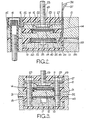
- the semi-conductor assembly includes first, second and third electrically conductive members 11, 12, 13 arranged one above the other, a semi-conductor device in the form of a diode 14 positioned between the members 11 and 12, and a further semi-conductor device in the form of a thyristor 15 positioned between the members 12 and 13.
- the second electrically conductive member 12 is defined by a rectangular aluminium block 21 having a cylindrical recess 22 extending inwardly from one face.
- the base of the recess 22 is formed with a centrally disposed upstanding circular plateau 23 upon the upper surface of which is positioned a molybdenum disc 24.
- the semi-conductor diode device 14 is seated on the disc 24 with its cathode in engagement with, and therefore in electrical connection with, the disc 24.
- the upwardly presented anode face of the diode 14 is engaged by a silver disc 25 and overlying the silver disc 25 is the first conductive member 11 in the form of a diaphragm plate formed from annealed copper.
- the diaphragm plate 11 has a circular recess 16 in its face remote from the washer 25, and within the recess 16 is a disc spring 26. Overlying the face of the plate 11 remote from the diode 14 is a top pressure plate 27 formed from brass. The central region of the disc spring 26 engages the base of the recess in the plate 11, and the periphery of the spring 26 engages the undersurface of the pressure plate 27. An electrically conductive bolt 28 extends upwardly through the pressure plate 27, the head of the bolt 28 being received in the recess 16. It will be recognised that the plate 27 and the plate 11 are in contact, and so are electrically interconnected, and similarly by virtue of their engagement with the bolt 28 the bolt 28 is electrically connected to the plates 11 and 27. Since the plate 11 is in contact with the silver washer 25 which in turn is in contact with th anode of the diode 14 then the bolt 28 constitutes an anode terminal for the diode 14.
- each fixing bolt 29 is equi-angularly spaced around the plate 27, and extend downwardly through corresponding apertures in the plates 27, and 11, and the base region of the block 21 to make screw-threaded engagement with corresponding screw-threaded bores in a bottom pressure plate positioned beneath the block 21 and constituting the third conductive member 13.
- the bottom pressure plate 13 is formed from brass, and since the bolts 29 are electrically conductive then the bottom pressure plate 13 and the top pressure plate 27 are electrically interconnected.
- the bores in the base region of the block 21 through which the bolts 29 pass are provided with electrically insulating lining sleeves 31 whereby the bolts 29.are electrically insulated from the second conductive member 12 and thus the block 21.
- a silver washer 32 one face of which engages the second conductive member 12.
- the semi-conductor thyristor device 15 Between the lower face of the washer 32 and the upper face of the pressure plate 13 and in axial alignment with the diode 14 is the semi-conductor thyristor device 15 the anode of which is in contact with the silver washer 32.
- the opposite face of the thyristor 15 is the cathode face of the thyristor, but within the cathode face is a surface area of the gate of the thyristor.
- the gate area is a circular area centrally disposed on the cathode face and the bottom pressure plate 13 has therein a centrally disposed circular recess 17 which ensures that the surface area of the pressure plate 13 which engages the cathode face of the thyristor 15 is an annular area engaging only the cathode of the thyristor.
- the gate contact area of the thyristor corresponds to the recess 17.
- the upstanding area of the pressure plate 13 which engages the thyristor is provided with a diametrically extending slot 18 which is lined with an electrically insulating member 33 of.U-shaped cross- section.
- Received by the member 33 so as to be insulated from the pressure plate 13 is a beryllium/copper beam connector 34 of known form.
- the beam connector 34 has a centrally disposed upward extension 35 ( Figure 2) which engages and makes electrical connection to the gate region of the thyristor 15.
- An electrically conductive lead 36 is connected at one end to the beam connector 34.
- the beam connector 34 is supported by the pressure plate 13 and makes electrical connection to the gate region of the thyristor, but is electrically insulated by the member 33 from the plate 13.
- the bolts 29 secure the assembly together in that they exert an axial clamping force pulling the pressure plate 13 towards the pressure plate 11 and thus trapping the intervening components on both sides of the second conductive member 12.
- the cathode of the diode 14 and the anode of the thyristor 15 are electrically interconnected by means of the second conductive member 12, and the anode of the diode 14 which is connected to the plate 11 is electrically connected by means of the bolts 29 to the cathode of the thyristor 15 by virtue of the engagement of the bolts 29 with the plate 13.
- the block 21 constitutes one terminal of the semi-conductor assembly, being electrically connected to the cathode of the diode and the anode of the thyristor, while the bolt 28 constitutes a second terminal of the assembly being electrically connected to the anode of the diode and the cathode of the thyristor.
- the thyristor gate connection of the assembly is made by way of the lead 36.
- a lead 37 is electrically connected to the pressure plate 13 to provide an additional electrical connection to the cathode of the thyristor 15.
- the assembly is completed by a further rectangular aluminium block 38 which lies beneath the block 21 and has therein a recess 39 receiving the thyristor and pressure plate 13 part of the assembly.
- the block 38 is electrically insulated from the block 21, and assembly mounting bolts 41 pass downwardly through the blocks 21 and 38 to make screw-threaded connection with a component upon which the assembly is mounted in use.
- the bolts 41 are electrically insulated from the blocks 21 and 38 by means of electrically insulating liners 42. Thus the securing bolts 41 do not electrically connect any part of the assembly to the component upon which the assembly is mounted.
- the recesses 22 and 39 are filled with an electrically insulating but thermally conductive encapsulant 43, conveniently an epoxy resin material loaded with aluminium particles.
- a suitable loaded resin material is available from Emerson & Cuming (UK) Limited, as"Eccobond 28481-6".
- rubber sealing elements 44, 45 are incorporated during construction of the assembly to encircle respectively the diode 14 and the thyristor 15.
- the sealing ring 44 is thus pinched between the top pressure plate 11 and the base of the recess in the block 21 while the sealing ring 45 is pinched between the base of the block 21 and the bottom pressure plate 13.
- the sealing ring 44, 45 constitute a physical barrier preventing the encapsulant 43 flowing onto the exposed regions of the semi-conductor devices.
- either or both of the mutually presented faces of the blocks 21 and 38 are provided with an anodized surface layer which serves to insulate the blocks from one another.
- the encapsulant 43 extends between the blocks 21 and 38 to provide an electrical insulation between the blocks.
- the block 21 constitutes the primary heat sink of the assembly.
- the block 38 is of course in intimate thermal (but not electrical) contact with the block 21 and thus effectively constitutes an increase in the mass of the block 21 for heat sink purposes.
- the exposed surface of the block 21 will be provided with an electrically insulating coating either by anodizing, or by covering with an insulating material.
- the intermediate metallic member 12 as the primary heat conductive path to the heat sink of-the assembly it is to be understood that the alumina loading in the encapsulant 43 ensures that the encapsulant has high thermal conductivity, and thus heat is conducted from the devices 14, 15 to the blocks 21 and 38 through the plates 11, 13 and 27 and through the encapsulant 43.
- the blocks 21 and 38 could be integral parts of the diaphragm plate 11 and pressure plate 13 respectively and having no connection to the intermediate conductive member 12. With such an arrangement a separate electrical connection must be brought out from the member 12.
- the heat sink can be provided primarily by the second conductive member 12 as is the case with the example illustrated, or alternatively could be provided by the first and third conductive members 11, 13, or as a further alternative could be provided by any one of the first, second and third conductive members alone or in combination with any one of the others.
- fluid cooling may be provided to reduce the heat sink bulk.
- the members constituting the heat sink may be drilled to receive a flow of cooling fluid or may be mounted in thermal contact with conduits carrying cooling fluid (for example one or more heat pipes).
Landscapes
- Thyristors (AREA)
- Die Bonding (AREA)
- Mechanical Treatment Of Semiconductor (AREA)
- Bipolar Transistors (AREA)
- Connections Arranged To Contact A Plurality Of Conductors (AREA)
Applications Claiming Priority (2)
| Application Number | Priority Date | Filing Date | Title |
|---|---|---|---|
| GB8221973 | 1982-07-29 | ||
| GB8221973 | 1982-07-29 |
Publications (2)
| Publication Number | Publication Date |
|---|---|
| EP0100626A2 true EP0100626A2 (de) | 1984-02-15 |
| EP0100626A3 EP0100626A3 (de) | 1985-11-06 |
Family
ID=10532002
Family Applications (1)
| Application Number | Title | Priority Date | Filing Date |
|---|---|---|---|
| EP83304199A Ceased EP0100626A3 (de) | 1982-07-29 | 1983-07-20 | Halbleiterzusammenbau |
Country Status (3)
| Country | Link |
|---|---|
| US (1) | US4642671A (de) |
| EP (1) | EP0100626A3 (de) |
| JP (1) | JPS5947754A (de) |
Cited By (5)
| Publication number | Priority date | Publication date | Assignee | Title |
|---|---|---|---|---|
| EP0182008A3 (en) * | 1984-10-15 | 1988-02-17 | Mitsubishi Denki Kabushiki Kaisha | Thyristor device with protection means |
| FR2614469A1 (fr) * | 1987-04-24 | 1988-10-28 | Inrets | Dispositif de refroidissement, en particulier pour semi-conducteur de puissance |
| WO1993014519A1 (en) * | 1992-01-15 | 1993-07-22 | General Electric Company | Gto module with stacked bypass diode |
| FR2715249A1 (fr) * | 1994-01-17 | 1995-07-21 | Saint Louis Inst | Dispositif de commutation particulièrement adapté aux tensions et courants élevés. |
| WO2016146086A3 (en) * | 2015-03-19 | 2017-01-12 | Ripd Research And Ip Development Ltd. | Devices for overvoltage, overcurrent and arc flash protection |
Families Citing this family (15)
| Publication number | Priority date | Publication date | Assignee | Title |
|---|---|---|---|---|
| JP3550243B2 (ja) * | 1996-01-30 | 2004-08-04 | 株式会社東芝 | 内部圧接型半導体装置 |
| US5866953A (en) * | 1996-05-24 | 1999-02-02 | Micron Technology, Inc. | Packaged die on PCB with heat sink encapsulant |
| US7233056B1 (en) * | 1998-02-23 | 2007-06-19 | Micron Technology, Inc. | Chip scale package with heat spreader |
| US6314639B1 (en) | 1998-02-23 | 2001-11-13 | Micron Technology, Inc. | Chip scale package with heat spreader and method of manufacture |
| US6297548B1 (en) | 1998-06-30 | 2001-10-02 | Micron Technology, Inc. | Stackable ceramic FBGA for high thermal applications |
| US6297960B1 (en) | 1998-06-30 | 2001-10-02 | Micron Technology, Inc. | Heat sink with alignment and retaining features |
| US6326687B1 (en) | 1998-09-01 | 2001-12-04 | Micron Technology, Inc. | IC package with dual heat spreaders |
| US6117797A (en) | 1998-09-03 | 2000-09-12 | Micron Technology, Inc. | Attachment method for heat sinks and devices involving removal of misplaced encapsulant |
| DE10009171B4 (de) * | 2000-02-26 | 2005-08-11 | Robert Bosch Gmbh | Stromrichter und sein Herstellverfahren |
| DE10258035A1 (de) * | 2002-12-12 | 2004-06-24 | Robert Bosch Gmbh | Einphasiges Stromrichtermodul |
| TWI339789B (en) * | 2006-09-29 | 2011-04-01 | Delta Electronics Inc | Device and heat sink |
| US20090103342A1 (en) * | 2007-10-17 | 2009-04-23 | Saul Lin | Silicon-controlled rectifier with a heat-dissipating structure |
| SG142321A1 (en) | 2008-04-24 | 2009-11-26 | Micron Technology Inc | Pre-encapsulated cavity interposer |
| DE112011105612B4 (de) * | 2011-09-13 | 2014-12-31 | Toyota Jidosha Kabushiki Kaisha | Halbleitermodul |
| US11776874B2 (en) * | 2020-03-24 | 2023-10-03 | Solaredge Technologies Ltd. | Apparatus and method for holding a heat generating device |
Family Cites Families (12)
| Publication number | Priority date | Publication date | Assignee | Title |
|---|---|---|---|---|
| FR2004508A1 (de) * | 1968-03-22 | 1969-11-28 | Mitsubishi Electric Corp | |
| US3743893A (en) * | 1971-05-27 | 1973-07-03 | Mitsubishi Electric Corp | Fluid cooled compression bonded semiconductor device structure |
| US3844029A (en) * | 1972-02-02 | 1974-10-29 | Trw Inc | High power double-slug diode package |
| US3992717A (en) * | 1974-06-21 | 1976-11-16 | Westinghouse Electric Corporation | Housing for a compression bonded encapsulation of a semiconductor device |
| DE2617335A1 (de) * | 1976-04-21 | 1977-11-03 | Siemens Ag | Halbleiterbauelement |
| DE2734571A1 (de) * | 1977-07-30 | 1979-02-15 | Bosch Gmbh Robert | Gleichrichteranordnung |
| FR2412168A1 (fr) * | 1977-12-15 | 1979-07-13 | Silicium Semiconducteur Ssc | Diodes ecreteuses de surtension |
| US4313128A (en) * | 1979-05-08 | 1982-01-26 | Westinghouse Electric Corp. | Compression bonded electronic device comprising a plurality of discrete semiconductor devices |
| US4305087A (en) * | 1979-06-29 | 1981-12-08 | International Rectifier Corporation | Stud-mounted pressure assembled semiconductor device |
| US4538171A (en) * | 1980-10-30 | 1985-08-27 | Cableform Limited | High power semiconductor heat sink assembly |
| JPS589349A (ja) * | 1981-07-10 | 1983-01-19 | Hitachi Ltd | Gtoスタツク |
| US4518983A (en) * | 1982-10-22 | 1985-05-21 | Westinghouse Electric Corp. | Assembly-heat sink for semiconductor devices |
-
1983
- 1983-07-20 EP EP83304199A patent/EP0100626A3/de not_active Ceased
- 1983-07-28 US US06/518,106 patent/US4642671A/en not_active Expired - Fee Related
- 1983-07-28 JP JP58136889A patent/JPS5947754A/ja active Pending
Cited By (9)
| Publication number | Priority date | Publication date | Assignee | Title |
|---|---|---|---|---|
| EP0182008A3 (en) * | 1984-10-15 | 1988-02-17 | Mitsubishi Denki Kabushiki Kaisha | Thyristor device with protection means |
| FR2614469A1 (fr) * | 1987-04-24 | 1988-10-28 | Inrets | Dispositif de refroidissement, en particulier pour semi-conducteur de puissance |
| WO1993014519A1 (en) * | 1992-01-15 | 1993-07-22 | General Electric Company | Gto module with stacked bypass diode |
| FR2715249A1 (fr) * | 1994-01-17 | 1995-07-21 | Saint Louis Inst | Dispositif de commutation particulièrement adapté aux tensions et courants élevés. |
| WO2016146086A3 (en) * | 2015-03-19 | 2017-01-12 | Ripd Research And Ip Development Ltd. | Devices for overvoltage, overcurrent and arc flash protection |
| US10447023B2 (en) | 2015-03-19 | 2019-10-15 | Ripd Ip Development Ltd | Devices for overvoltage, overcurrent and arc flash protection |
| US11527879B2 (en) | 2015-03-19 | 2022-12-13 | Ripd Ip Development Ltd | Devices for overvoltage, overcurrent and arc flash protection |
| US12003088B2 (en) | 2015-03-19 | 2024-06-04 | Ripd Ip Development Ltd | Devices for overvoltage, overcurrent and arc flash protection |
| US12322949B2 (en) | 2015-03-19 | 2025-06-03 | Ripd Ip Development Ltd | Devices for overvoltage, overcurrent and arc flash protection |
Also Published As
| Publication number | Publication date |
|---|---|
| EP0100626A3 (de) | 1985-11-06 |
| US4642671A (en) | 1987-02-10 |
| JPS5947754A (ja) | 1984-03-17 |
Similar Documents
| Publication | Publication Date | Title |
|---|---|---|
| US4642671A (en) | Semi-conductor assembly | |
| US3573574A (en) | Controlled rectifier mounting assembly | |
| US5006921A (en) | Power semiconductor switching apparatus with heat sinks | |
| US4700273A (en) | Circuit assembly with semiconductor expansion matched thermal path | |
| US9572291B2 (en) | Semiconductor device and method for manufacturing same | |
| US5297001A (en) | High power semiconductor assembly | |
| US3471757A (en) | Semiconductor rectifier assembly | |
| WO1985002087A1 (en) | Semiconductor package with internal heat exchanger | |
| WO2016165843A1 (en) | Power electronics module | |
| US4313128A (en) | Compression bonded electronic device comprising a plurality of discrete semiconductor devices | |
| US4518982A (en) | High current package with multi-level leads | |
| US3293508A (en) | Compression connected semiconductor device | |
| US6452261B1 (en) | Flat semiconductor device and power converter employing the same | |
| US12249561B2 (en) | Semiconductor device arrangement with compressible adhesive | |
| US20030122261A1 (en) | Power semiconductor submodule, and a power semiconductor module | |
| US3525910A (en) | Contact system for intricate geometry devices | |
| JPH08306856A (ja) | マルチチップ・パッケージの作成方法 | |
| US3328650A (en) | Compression bonded semiconductor device | |
| US6340927B1 (en) | High thermal efficiency power resistor | |
| US3313987A (en) | Compression bonded semiconductor device | |
| US7229855B2 (en) | Process for assembling a double-sided circuit component | |
| CN111081664A (zh) | 具有用于热性能的相变材料的半导体器件的封装 | |
| US3450962A (en) | Pressure electrical contact assembly for a semiconductor device | |
| US6291878B1 (en) | Package for multiple high power electrical components | |
| US20240213106A1 (en) | Semiconductor device |
Legal Events
| Date | Code | Title | Description |
|---|---|---|---|
| PUAI | Public reference made under article 153(3) epc to a published international application that has entered the european phase |
Free format text: ORIGINAL CODE: 0009012 |
|
| AK | Designated contracting states |
Designated state(s): DE FR GB IT |
|
| 17P | Request for examination filed |
Effective date: 19840717 |
|
| RAP1 | Party data changed (applicant data changed or rights of an application transferred) |
Owner name: LUCAS INDUSTRIES PUBLIC LIMITED COMPANY |
|
| D17P | Request for examination filed (deleted) | ||
| PUAL | Search report despatched |
Free format text: ORIGINAL CODE: 0009013 |
|
| AK | Designated contracting states |
Designated state(s): DE FR GB IT |
|
| R17P | Request for examination filed (corrected) |
Effective date: 19860502 |
|
| 17Q | First examination report despatched |
Effective date: 19880407 |
|
| STAA | Information on the status of an ep patent application or granted ep patent |
Free format text: STATUS: THE APPLICATION HAS BEEN REFUSED |
|
| 18R | Application refused |
Effective date: 19881007 |
|
| RIN1 | Information on inventor provided before grant (corrected) |
Inventor name: ROHSLER, IVOR CARL Inventor name: CLARK, ANTHONY FREDERICK CAREY |