EP0100825A2 - Echte Einfachfehlerkorrektur und Mehrfehlererkennungssystem - Google Patents
Echte Einfachfehlerkorrektur und Mehrfehlererkennungssystem Download PDFInfo
- Publication number
- EP0100825A2 EP0100825A2 EP83104955A EP83104955A EP0100825A2 EP 0100825 A2 EP0100825 A2 EP 0100825A2 EP 83104955 A EP83104955 A EP 83104955A EP 83104955 A EP83104955 A EP 83104955A EP 0100825 A2 EP0100825 A2 EP 0100825A2
- Authority
- EP
- European Patent Office
- Prior art keywords
- bits
- bit
- error
- data
- syndrome
- Prior art date
- Legal status (The legal status is an assumption and is not a legal conclusion. Google has not performed a legal analysis and makes no representation as to the accuracy of the status listed.)
- Ceased
Links
Images
Classifications
-
- G—PHYSICS
- G06—COMPUTING OR CALCULATING; COUNTING
- G06F—ELECTRIC DIGITAL DATA PROCESSING
- G06F11/00—Error detection; Error correction; Monitoring
- G06F11/07—Responding to the occurrence of a fault, e.g. fault tolerance
- G06F11/08—Error detection or correction by redundancy in data representation, e.g. by using checking codes
- G06F11/10—Adding special bits or symbols to the coded information, e.g. parity check, casting out 9's or 11's
- G06F11/1008—Adding special bits or symbols to the coded information, e.g. parity check, casting out 9's or 11's in individual solid state devices
- G06F11/1012—Adding special bits or symbols to the coded information, e.g. parity check, casting out 9's or 11's in individual solid state devices using codes or arrangements adapted for a specific type of error
- G06F11/1028—Adjacent errors, e.g. error in n-bit (n>1) wide storage units, i.e. package error
Definitions
- This invention relates to the correction of errors in data words stored in a data storage system and in particular, to a true single error correction and multiple error detection system.
- the present invention finds particular utility in high density integrated circuit storage arrays. Developments in memory technology have resulted in storage chips having the capacity to store multiple data bits per chip with corresponding multiple outputs. Errors in the storage of data in these memories are generally classified as occurring due to two distinct causes. One is a non-destructive environmental phenomenon caused by impingement of atomic alpha particles. Those particles, present in ordinary background atomic radiation, have energy values vis-a-vis the data signal stored in the cell. When such cells are struck by atomic alpha particles, the binary values stored in the cell may flip to an opposite value. Hence a data error occurs. These errors are therefore transient, that is, intermittent errors, and are delineated as "soft" errors. The second major cause of error is the actual physical failure of one of the memory components. This failure produces a permanent or "hard” error.
- ECC error correcting codes
- SEC/DED single error correction - double error detection
- the error correcting scheme should also not require extensive logic circuitry. Additional circuitry slows overall processing or throughput time of the system and incurs a penalty of requiring additional processing space in an already crowded environment of integrated circuits. A usable system should therefore minimize the need for external logic circuits for ECC processing.
- the H-Matrix is a code having minimum weight w so that every combination of w - 1 or fewer columns of the matrix is linearly independent.
- the minimum weight requirement is recognized in the prior art as 4, thereby requiring that 3 or fewer columns of the H-Matrix be linearly independent.
- Three constraints are imposed by Hsiao in the generation of the H-Matrix. First, each column has an odd number of ones, that is, all column vectors are of odd weight. Secondly, the total number of ones in the H-Matrix should be minimized. Thirdly, the number of ones in each row of matrix should be equal or as close as possible to the average number, that is, the total number of ones in the matrix divided by the total number of rows.
- N°42966 Reference is also made to European Patent Application! which extends the Hsiao teaching into a system dividing the data word into high and low density storage units.
- high density storage module is used to receive the data portion of the word and a low density unit receives the check bits forming the remaining portion of the data word.
- the invention proceeds from the assumption that soft errors will not occur in the low density storage unit and accordingly, the check bits are assumed to be correct. Consequently, the number of check bits can be reduced such that in a 16 data bit word only 5 check bits are needed.
- Such a system while offering important advantages in the reduction of the number of bits of storage required, is not architecturally configured for an efficient implementation in a multiple bit per chip system. That is, this ECC is applied to a "by 1" storage system.
- U.S. Patent 3,656,107 relates to a method of detecting and correcting double errors by generating a specific set of syndrome S bits. If a double error occurs in a binary word, the syndrome S bits automatically operate a switching device which changes the bits of the binary word one at a time to correct one of the double errors. This correction is effectuated until the syndrome indicates that the double error has been eliminated. A new syndrome is then generated to locate the single remaining error.
- U.S. Patent 4,005,405 discloses a modified ECC utilizing 5 check bits for a 26 bit data word. Double error detection and therefore the ability to locate multiple bit failures is not perceived.
- U.S. Patent 4,139,148 employs a SEC/DED with a divided common RAM with separate data and check bit locations.
- the H-Matrix and to hardware implementation employs 7 check bits for 38 data bits.
- Various coding parameters for the determination of the H-Matrix follows the known Hsiao technique. Correction of double bit errors is attained by saving previously occurring single error syndromes and using them to correct one error bit when a double bit error occurs in the single word in storage.
- Another object of this invention is to define a true single error correction system that will detect multiple bit failures and yet will not miscorrect single bits.
- a single error correction, multiple error detection system for data words stored in a memory having multiple data bits per chip, comprising a check bit generator receiving data bits and generating check bits in accordance with logical sequence, a syndrome bit generator for generating syndrome bits from the data and check bits, first logic receiving each of the syndrome bits and producing an output for determining the presence of a true single error in one of the data and check bits, and a second logic receiving each of the syndrome bits and the output of the first logic for detecting the presence of multiple bit error in the absence of a single bit error detected at the output of the first logic.
- the first logic employs error locators processing The syndrome bits such that a determination of single bit failure is first made. If a single bit error has occurred, then the corresponding error locator is used to block an error indicator such that only a single bit failure can turn a particular circuit on.
- syndrome bits are therefore fed to a second logic such that the presence of an output coupled with an error locator output indicates a multiple failure.
- FIG. 1 is a diagram of the H-Matrix for a true single error correction and double error detection in accordance with the present invention.
- FIG. 2 is a schematic diagram of an implementation of the present invention.
- the present invention is directed specifically to high density arrays having multiple data bits in a high density chip.
- An example is an array of 16Kx9 chips.
- the "by 9" offering of such a chip perceives that multiple bit errors may occur and that such errors may in fact be odd numbered multiple bit failures.
- the use of conventional SEC/ DE D systems will erroneously miscorrect single data bits that are, in fact, not in error due to the fact that a syndrome may be allocated for a single bit data error as a result of a combination of an odd multiple bit failure within a chip. That is, utilizing conventional detecting code schemes, a syndrome allocated for a particular single data bit may be generated as a consequence of an odd multiple bit failure not involving that correct data bit.
- the 16, 6 code is inefficient with the "by 9" offering since 5 bits of a 27 bit word are not utilized. That is, the prior art use of six check bits will result in surplus bits in each data word.
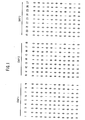
- Figure 1 shows an H-Matrix for true single error correction and double error detection in accordance with this invention.
- This H-Matrix is logically organized on three "by 9" chips. The organization utilizes the standard 16 data bit per data word format but employs 11 check bits.
- the H-Matrix of Figure 1 is shown as used conventionally in, for example, Hsiao, supra. and in the Encyclopedia of Computer Science, Ralston and Meek, 1976, pp. 547-548.
- Figure 1 is a hardware map defining the manner in which the parity generating circuits and parity checking circuits are constructed to perform true single error correction and double error detection.
- the "1" marks in any horizontal row denote bits which need to be checked by a particular parity checking circuit.
- the H-Matrix of Figure 1 satisfies the construction rules set forth in the above patent that each information and check bit be assigned in an odd number of code groups. That is, each column has an odd number of ones so that all column vectors are-of odd weight. Secondly, the total number of ones in the H-Matrix is minimized. Finally, the number of ones in each row of the matrix is approximately equal to or as close as possible to the average number, that is, the total number of ones in the matrix divided by the total number of rows. By inspection, the H-Matrix has 59 "ones" in 11 rows or an average of approximately 5.5 ones per row. No row has less than 4 ones or more than 6.
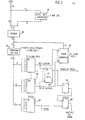
- Each data word comprises 16 data bits.
- the notation "/" indicates the number of bit lines in a particular data bus.
- the 16 bit data word (/16) is supplied to a check bit generator 10 comprising a number of 3-way Exclusive-OR circuits.
- the check bit generator 10 provides an output in the form of 11 check bits which are then combined with the 16 bit data word to form a 27 bit data word stored on three "by 9" chips.
- the 27 bit word is delivered to a syndrome bit generator (30) that performs 11 parity checks.
- the parity check circuits comprise one circuit for each check bit.
- Figure 2 utilizes separate circuitry for the check bit generator and the syndrome bit generator (30), it is apparent that the same set of Exclusive-OR (EOR) circuits can be used to provide both check bit generation and syndrome bit generation function. If such a mode of implementation were used, a switching circuit would be needed to switch the EOR circuits from a storage writing operation to a storage read out operation. However, to eliminate the extra switching circuits, the technology generally employs separate circuitry.
- EOR Exclusive-OR
- Single bit correction is accomplished in a manner known in the technology using an error corrector.
- the inputs to the error corrector are different than in the prior art. That is, the error corrector receives outputs corresponding to the outputs of 27 error locators 40 each receiving the 11 syndrome bits to indicate a single error position.
- the error corrector 60 comprising 27 2-way EOR circuits receives also each of the 27 bits from storage. Only one of the error locator outputs will have a "1" level corresponding to the one erroneous bit position. That particular signal on the output line is used by the corrector to correct the erroneous output bit by inversion to an opposite binary value.
- the present invention utilizing the H-Matrix of Figure 1 includes extra logic in the correction circuitry to determine whether a single bit failure has occurred or if a multiple bit failure is indicated.
- the H-Matrix insures that syndromes generated by the syndrome bit generators 30 by multiple bit failures will not match any of the syndromes for a single bit failure. Accordingly, the H-Matrix affirmatively precludes miscorrection of data bits that have not failed.
- error locators 40 comprising 27 11-way AND gates receive the 11 syndrome bits generated by the syndrome bit generator.
- This correction circuitry checks the syndromes and determines if the syndrome is all zeros or if an output matches one from the H-Matrix. If the syndrome output is all zeros, then no failure has occurred. If, however, a positive output occurs, then matching with the H-Matrix indicates whether a single bit failure has occurred at that bit position.
- the 27 lI-way ANDs produce 27 bit locator outputs.
- the error locator circuits 40 therefore all receive inputs from all 11 syndrome bits. This is a departure from prior SEC/DED schemes for only the syndrome bits which are coded binary "1" feed each error locator. Consequently, the system in Figure 2 insures that multiple errors will not activate an incorrect locator.
- the bit locator outputs are fed to an error corrector 60 comprising 27 2-way EORs. Accordingly, by using all 11 syndrome bits in each error locator, only a single bit failure will actuate a particular circuit. This represents a simplification from logic used in some SEC/DED error indicators where the syndrome bits must be exclusively EORed.
- the 27 locator bit outputs are also fed to a 27-way locator OR gate 50 so that any output indicates the presence of an error. That OR output is then inverted in inverter 70 and fed to an escape detector AND gate 80.
- An escape OR gate 90 receives the 11 syndrome bits such that an output indicates that a failure has occurred. As indicated, if the single bit error has occurred, a corresponding error locator will also be on, however the syndromes are unique for only a single bit error. Any output from the escape OR 90 then represents a multiple bit failure if an error locator OR is "off".
- the escape OR output is fed to the escape AND gate 80 receiving the inverted output of the ORed output of the 27 bit locators 40.
- a multiple bit error is signaled by the presence of one or more syndrome bit ones from the escape OR 90 gate coupled with a zero level, inverted output, i.e. a level one output from the inverter 70.
- the present invention therefore represents a significant improvement over the prior art since it positively detects all escapes for 9 bit memory chips. It also attains this positive indication in a single pass through the combinational logic of Figure 2. Importantly, the implementation of Figure 2 allows for true single error correction while preventing all escapes.
Landscapes
- Engineering & Computer Science (AREA)
- Theoretical Computer Science (AREA)
- Quality & Reliability (AREA)
- Physics & Mathematics (AREA)
- General Engineering & Computer Science (AREA)
- General Physics & Mathematics (AREA)
- Detection And Correction Of Errors (AREA)
- Techniques For Improving Reliability Of Storages (AREA)
Applications Claiming Priority (2)
| Application Number | Priority Date | Filing Date | Title |
|---|---|---|---|
| US39106282A | 1982-06-22 | 1982-06-22 | |
| US391062 | 1982-06-22 |
Publications (2)
| Publication Number | Publication Date |
|---|---|
| EP0100825A2 true EP0100825A2 (de) | 1984-02-22 |
| EP0100825A3 EP0100825A3 (de) | 1987-05-06 |
Family
ID=23545066
Family Applications (1)
| Application Number | Title | Priority Date | Filing Date |
|---|---|---|---|
| EP83104955A Ceased EP0100825A3 (de) | 1982-06-22 | 1983-05-19 | Echte Einfachfehlerkorrektur und Mehrfehlererkennungssystem |
Country Status (3)
| Country | Link |
|---|---|
| EP (1) | EP0100825A3 (de) |
| JP (1) | JPS593645A (de) |
| CA (1) | CA1184308A (de) |
Cited By (4)
| Publication number | Priority date | Publication date | Assignee | Title |
|---|---|---|---|---|
| FR2594976A1 (fr) * | 1986-02-25 | 1987-08-28 | Philips Nv | Systeme de memoire a trois modules construit a l'aide de puces de memoire d'une largeur d'un symbole et presentant une caracteristique de protection entre les erreurs, chaque symbole etant constitue de 2i + 1 bits |
| EP0236053A3 (en) * | 1986-03-03 | 1989-03-29 | Unisys Corporation | Memory system employing a zero dc power gate array for error correction |
| EP0236052A3 (de) * | 1986-03-03 | 1989-03-29 | Unisys Corporation | Speichersystem unter Benutzung eines Gatterfeldes niedriger Gleichstromleistung zur Fehlerkorrektur |
| JP2012198727A (ja) * | 2011-03-20 | 2012-10-18 | Fujitsu Ltd | メモリコントローラ及び情報処理装置 |
Family Cites Families (1)
| Publication number | Priority date | Publication date | Assignee | Title |
|---|---|---|---|---|
| US4334309A (en) * | 1980-06-30 | 1982-06-08 | International Business Machines Corporation | Error correcting code system |
-
1983
- 1983-04-06 CA CA000425351A patent/CA1184308A/en not_active Expired
- 1983-05-10 JP JP58080214A patent/JPS593645A/ja active Pending
- 1983-05-19 EP EP83104955A patent/EP0100825A3/de not_active Ceased
Cited By (4)
| Publication number | Priority date | Publication date | Assignee | Title |
|---|---|---|---|---|
| FR2594976A1 (fr) * | 1986-02-25 | 1987-08-28 | Philips Nv | Systeme de memoire a trois modules construit a l'aide de puces de memoire d'une largeur d'un symbole et presentant une caracteristique de protection entre les erreurs, chaque symbole etant constitue de 2i + 1 bits |
| EP0236053A3 (en) * | 1986-03-03 | 1989-03-29 | Unisys Corporation | Memory system employing a zero dc power gate array for error correction |
| EP0236052A3 (de) * | 1986-03-03 | 1989-03-29 | Unisys Corporation | Speichersystem unter Benutzung eines Gatterfeldes niedriger Gleichstromleistung zur Fehlerkorrektur |
| JP2012198727A (ja) * | 2011-03-20 | 2012-10-18 | Fujitsu Ltd | メモリコントローラ及び情報処理装置 |
Also Published As
| Publication number | Publication date |
|---|---|
| EP0100825A3 (de) | 1987-05-06 |
| JPS593645A (ja) | 1984-01-10 |
| CA1184308A (en) | 1985-03-19 |
Similar Documents
| Publication | Publication Date | Title |
|---|---|---|
| EP0042966B1 (de) | System und Verfahren zur Fehlererkennung und Fehlerkorrektur von gespeicherten digitalen Daten | |
| US4175692A (en) | Error correction and detection systems | |
| EP0261031B1 (de) | Verfahren und Gerät zur Fehlerkorrektur in einem aus parallelem Prozessor bestehenden Datenverarbeitungssystem | |
| US5177744A (en) | Method and apparatus for error recovery in arrays | |
| US6662333B1 (en) | Shared error correction for memory design | |
| US4740968A (en) | ECC circuit failure detector/quick word verifier | |
| US3755779A (en) | Error correction system for single-error correction, related-double-error correction and unrelated-double-error detection | |
| US4335459A (en) | Single chip random access memory with increased yield and reliability | |
| US5907671A (en) | Fault tolerant system based on voting | |
| EP0186719B1 (de) | Gerät zum Korrigieren von Fehlern in Speichern | |
| EP0195445B1 (de) | Halbleiterspeichergerät mit einer Korrekturfunktion | |
| EP0077204B1 (de) | Fehlerkorrekturspeicher mit geringem zusätzlichem Platzbedarf und schnellem Korrekturmechanismus | |
| EP0463210B1 (de) | Verfahren und Vorrichtung zur Prüfung des Inhalts und der Adresse einer Speicheranordnung | |
| US4456980A (en) | Semiconductor memory device | |
| EP0141498A2 (de) | Gerät zur Verringerung des zur Fehlererkennung- und Korrektur erforderlichen Speichers in Datenverarbeitungsmaschinen | |
| US5757823A (en) | Error detection and correction for four-bit-per-chip memory system | |
| US4942575A (en) | Error connection device for parity protected memory systems | |
| US4236247A (en) | Apparatus for correcting multiple errors in data words read from a memory | |
| US5751745A (en) | Memory implemented error detection and correction code with address parity bits | |
| US6574746B1 (en) | System and method for improving multi-bit error protection in computer memory systems | |
| US5491702A (en) | Apparatus for detecting any single bit error, detecting any two bit error, and detecting any three or four bit error in a group of four bits for a 25- or 64-bit data word | |
| US6463563B1 (en) | Single symbol correction double symbol detection code employing a modular H-matrix | |
| EP0100825A2 (de) | Echte Einfachfehlerkorrektur und Mehrfehlererkennungssystem | |
| EP0310220B1 (de) | Gerät zur Korrektur von einfachen Bitfehlern und zur Erkennung von doppelten Bitfehlern bei Datenübertragung | |
| US6519735B1 (en) | Method and apparatus for detecting errors in data output from memory and a device failure in the memory |
Legal Events
| Date | Code | Title | Description |
|---|---|---|---|
| PUAI | Public reference made under article 153(3) epc to a published international application that has entered the european phase |
Free format text: ORIGINAL CODE: 0009012 |
|
| AK | Designated contracting states |
Designated state(s): DE FR GB |
|
| 17P | Request for examination filed |
Effective date: 19840426 |
|
| PUAL | Search report despatched |
Free format text: ORIGINAL CODE: 0009013 |
|
| AK | Designated contracting states |
Kind code of ref document: A3 Designated state(s): DE FR GB |
|
| 17Q | First examination report despatched |
Effective date: 19880511 |
|
| STAA | Information on the status of an ep patent application or granted ep patent |
Free format text: STATUS: THE APPLICATION HAS BEEN REFUSED |
|
| 18R | Application refused |
Effective date: 19920202 |
|
| RIN1 | Information on inventor provided before grant (corrected) |
Inventor name: CHISHOLM, DOUGLAS RODERICK Inventor name: SUAREZ, GUSTAVO ARMANDO Inventor name: BHANSALI, MAHENDRA MULCHANDBHAI Inventor name: MINNICH, WALTER DALE Inventor name: FINNEY, DAMON W. Inventor name: BANNON, ROBERT DANIEL |