EP0100933B1 - Méthode et dispositif pour le traitement d'une pièce d'usinage par un rayon électronique focalisé - Google Patents
Méthode et dispositif pour le traitement d'une pièce d'usinage par un rayon électronique focalisé Download PDFInfo
- Publication number
- EP0100933B1 EP0100933B1 EP83107091A EP83107091A EP0100933B1 EP 0100933 B1 EP0100933 B1 EP 0100933B1 EP 83107091 A EP83107091 A EP 83107091A EP 83107091 A EP83107091 A EP 83107091A EP 0100933 B1 EP0100933 B1 EP 0100933B1
- Authority
- EP
- European Patent Office
- Prior art keywords
- electron beam
- modulation
- path
- frequency
- workpiece
- Prior art date
- Legal status (The legal status is an assumption and is not a legal conclusion. Google has not performed a legal analysis and makes no representation as to the accuracy of the status listed.)
- Expired
Links
- 238000010894 electron beam technology Methods 0.000 title claims description 86
- 238000000034 method Methods 0.000 title claims description 42
- 238000003466 welding Methods 0.000 claims description 31
- 230000015654 memory Effects 0.000 claims description 22
- 230000006870 function Effects 0.000 claims description 5
- 238000012545 processing Methods 0.000 claims description 4
- 239000000872 buffer Substances 0.000 claims description 3
- 230000008859 change Effects 0.000 claims description 2
- 230000004927 fusion Effects 0.000 claims 6
- 230000004907 flux Effects 0.000 claims 1
- 230000008018 melting Effects 0.000 description 19
- 238000002844 melting Methods 0.000 description 19
- 230000000875 corresponding effect Effects 0.000 description 10
- 230000008569 process Effects 0.000 description 9
- 230000015572 biosynthetic process Effects 0.000 description 8
- 239000000463 material Substances 0.000 description 8
- 239000000155 melt Substances 0.000 description 6
- 239000012071 phase Substances 0.000 description 6
- 230000008020 evaporation Effects 0.000 description 4
- 238000001704 evaporation Methods 0.000 description 4
- 239000011324 bead Substances 0.000 description 3
- 230000001276 controlling effect Effects 0.000 description 3
- 238000009826 distribution Methods 0.000 description 3
- 230000000694 effects Effects 0.000 description 3
- 238000011835 investigation Methods 0.000 description 3
- 230000006978 adaptation Effects 0.000 description 2
- 238000009499 grossing Methods 0.000 description 2
- 230000001788 irregular Effects 0.000 description 2
- 238000003754 machining Methods 0.000 description 2
- 230000000750 progressive effect Effects 0.000 description 2
- 239000011343 solid material Substances 0.000 description 2
- 230000007704 transition Effects 0.000 description 2
- 229910000746 Structural steel Inorganic materials 0.000 description 1
- 230000001133 acceleration Effects 0.000 description 1
- 230000003321 amplification Effects 0.000 description 1
- 239000003990 capacitor Substances 0.000 description 1
- 238000004590 computer program Methods 0.000 description 1
- 230000008878 coupling Effects 0.000 description 1
- 238000010168 coupling process Methods 0.000 description 1
- 238000005859 coupling reaction Methods 0.000 description 1
- 230000001419 dependent effect Effects 0.000 description 1
- 238000011161 development Methods 0.000 description 1
- 230000018109 developmental process Effects 0.000 description 1
- 238000010586 diagram Methods 0.000 description 1
- 238000002474 experimental method Methods 0.000 description 1
- 230000002349 favourable effect Effects 0.000 description 1
- 239000012530 fluid Substances 0.000 description 1
- 238000010438 heat treatment Methods 0.000 description 1
- 210000001503 joint Anatomy 0.000 description 1
- 239000007788 liquid Substances 0.000 description 1
- 238000005259 measurement Methods 0.000 description 1
- 238000003199 nucleic acid amplification method Methods 0.000 description 1
- 238000005457 optimization Methods 0.000 description 1
- 230000010355 oscillation Effects 0.000 description 1
- 230000010363 phase shift Effects 0.000 description 1
- 238000007711 solidification Methods 0.000 description 1
- 230000008023 solidification Effects 0.000 description 1
- 239000012808 vapor phase Substances 0.000 description 1
Images

Classifications
-
- B—PERFORMING OPERATIONS; TRANSPORTING
- B23—MACHINE TOOLS; METAL-WORKING NOT OTHERWISE PROVIDED FOR
- B23K—SOLDERING OR UNSOLDERING; WELDING; CLADDING OR PLATING BY SOLDERING OR WELDING; CUTTING BY APPLYING HEAT LOCALLY, e.g. FLAME CUTTING; WORKING BY LASER BEAM
- B23K15/00—Electron-beam welding or cutting
- B23K15/02—Control circuits therefor
Definitions
- the invention relates to a method and an arrangement for machining, in particular welding, heating, remelting a workpiece by means of a focused electron beam, the point of impact of which moves relative to the workpiece on a predetermined path curve and is additionally deflected relative to the path curve on a modulation curve superimposed on the path curve.
- this also includes two parts lying opposite each other on a butt surface, which are to be welded together along the butt joint.
- both the trajectory curve and the modulation curve are represented by analytical functions with the aid of corresponding function generators. Only very special curves such as straight lines, circles, parabolas and the like can be analyzed. Generate the like, which become zigzag or spiral figures as the beam travels along the trajectory.
- the analytical functions that can be combined to form certain curve types are run through at a certain path speed that is dependent on the curve display and cannot be set.
- the electron beam striking the workpiece transfers its energy in the form of heat to the workpiece and heats it up locally above the melting and evaporation temperature.
- the result is a melting zone, which is separated from the solid material by a phase boundary, and a vapor capillary arranged within the melting zone in the direct area of impact of the electron beam.
- the phase boundary between the vapor capillary and the melt is essentially due to the energetic equilibrium conditions in the border area.
- the invention is therefore based on the object to improve the known method of the type mentioned in such a way that arbitrary curve domes for modulating the electron beam along the trajectory can be made available, with regard to the shape and amplitude as well as with regard to the direction and speed of the Electron beam are optimally adaptable to the flow conditions in the melting zone.
- the point-by-point representation of the modulation curve with regard to both the curve shape and the path speed along the curve allows a large scope for an optimal adaptation to the material and geometric conditions of the machining process.
- the electron beam movement is adapted to the flow conditions in the melting zone in that the modulation curve is essentially mirror-symmetrical to the path curve tangent and is traversed by the electron beam in mirror-symmetrical directions to the path curve tangent.
- the electron beam is briefly stopped at the individual support points. It has proven to be advantageous if the electron beam is moved continuously between two support points on an interpolation path delimited by the support points.
- the path speed along the modulation curve can be varied simply by arranging the support points at a corresponding variable distance from one another: the closer the support points are in a certain curve area, the slower the electron beam traverses this area.
- the location coordinates of the individual support points are read out sequentially from a digital memory arrangement, converted into an analog current and voltage signal and in this form fed to the deflection coils or plates for the electron beam.
- the amplitudes of the analog signals assigned to the coordinates of the individual support points are expediently smoothed in a filter arrangement arranged in front of the deflection coils or plates, the cut-off frequency of which is a function, preferably a multiple, of the trigger frequency.
- the focus position and / or the beam current intensity can also be varied along the modulation curve.
- the control data for the focus position and / or the beam current intensity assigned to the individual support points of the modulation curve are read out sequentially from a digital memory arrangement, like the coordinates, converted into an analog signal and in this form, if necessary after smoothing in a filter arrangement, for focusing and / or Beam current control of the electron beam used.
- a switching arrangement which contains at least two data memories for the X and Y coordinate values of the modulation curve, the address lines of which, together with the counting output, preferably by a clock generator with a clock frequency between 10 kHz and 10 MHz between 100 kHz and 1 MHz, driven counter and their data lines are connected to the input of each of the respective deflection coils or plates of the electron beam processing machine controlling digital / analog converter.
- CMOS RAMs CMOS random access memories
- the circuit arrangement shown in FIG. 1 is an additional device for an electron beam welding machine, in which the point of incidence of a focused electron beam is moved on a predetermined trajectory relative to the workpiece to be welded. It is irrelevant whether the relative movement is caused by moving the workpiece or by corresponding movement of the electron beam.
- the circuit arrangement generates a modulation or pendulum curve, along which the electron beam is deflected in relation to the path curve in the course of the welding process.
- the x and y coordinates of the modulation curve are stored point by point in digital form in the data memories 110, 112 and can be read out sequentially from them in continuous cycles.
- Both the read memories (ROMs) and the CMOS read and write memories (CMOS RAMs) shown can be considered as data memories.
- the coordinate values are read out from the data memories via a binary counter 116, the counting outputs of which are connected to the address lines of the memories 110, 112.
- the clock input of the counter 116 is controlled via the output signal of a clock generator 118, the clock frequency of which can be set with the aid of a reading element 120 which can be operated manually, electronically or by machine.
- the data lines of the memories 110, 112 are connected to the input buffer 122, 124 each of a digital / analog converter 128/130, which is driven by a signal whose frequency matches the clock signal, but at least by one of the access times of the read memory 110, 112 corresponding time is out of phase.
- the phase shift can take place either with the delay element 134 (monoflop) or by the fact that the counter 116 responds to the leading edge and the input buffers 122, 124 to the trailing edge of the rectangular clock signal.
- the analog output signals of the digital / analog converter 128, 130 are each smoothed in a low-pass filter arrangement 136, 138, so that there is a continuous transition between the support points of the modulation curve.
- the limit frequencies of the filter arrangement 136, 138 must be adapted to the respective clock frequency so that the transition areas between the support points are evenly traversed even at different clock frequencies (web speeds).
- this adaptation can be carried out by simultaneously adjusting the resistance and / or the capacitance values in the filter arrangements 136, 138 with the adjustment of the clock frequency via the reading element 120, as indicated by the dash-dotted signal line 142 .
- a significantly lower circuit complexity results when using charge-coupled filters (switched capacitor filters), which are available as integrated circuits. These are higher order filters with frequency controlled resistors.
- the cut-off frequency can be controlled there directly via the clock frequency with the interposition of a frequency multiplier 144. This results in a direct coupling between the clock frequency set on the clock generator and the cutoff frequency of the filter arrangements, the cutoff frequency being a certain multiple, e.g. B. is one hundred times the clock frequency.
- An additional electronic circuit arrangement 146 is connected downstream of the filters 136, 138, by means of which the position of the modulation figure in the coordinate system can preferably be rotated in 4 steps of 90 ° and the direction of rotation can be changed in the case of symmetrical curves.
- the analog signals generated in this way are fed to the amplifiers 148, 150 of the X and Y deflection coils 154, 156 of the electron beam welding machine.
- a variation of a third coordinate is provided, which can consist in controlling the focus position of the electron beam or in controlling the beam current intensity depending on the position on the modulation curve.
- the relevant coordinate values are in turn digitally contained in a data memory 114, from which they can be read out sequentially with the aid of the counter 116 and converted into analog signals via the digital / analog converter 126, 132.
- the signals are fed to the amplifier 152 of the focusing lens 158 or to a beam current control (not shown) of the electron beam welding machine.
- the coordinate sets of a larger number of different modulation curves can be accommodated in the data memories 110, 112, 114 in different address areas.
- the relevant address areas can be controlled via a second reading element 160 which can be operated manually or by machine.
- the counting range of the counter 116 for each selected modulation curve can also be adjusted via the reading element 160, provided that the number of support points in the stored modulation curves should be different.
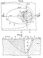
- v means the feed speed of the workpiece relative to the point of impact.
- the electron beam b striking the workpiece transfers its energy in the form of heat to the workpiece 10 and heats it locally above the melting and evaporation temperature.
- the result is a melting zone 14, which is separated from the solid material by the phase boundary 16, and a vapor capillary 20, which is arranged within the melting region 14 in the direct impact area of the electron beam, the phase boundary 22 of which is essentially due to the energetic equilibrium conditions in the boundary region.
- FIGS. 2a and b The temperature profile shown in FIGS. 2a and b is the result of a theoretical investigation of the processes involved in welding with an uncoupled electron beam on a moving workpiece under stationary conditions.
- 2a is a plan view of the workpiece surface (xy plane) and in FIG. 2b a vertical section along the plane of symmetry spanned by the trajectory tangent 12 (x axis) and the beam direction b (z axis) (xz plane) shown.
- the material data of a fine-grained structural steel (22 MnMoNi 55) were used (melting temperature 1 500 ° C, evaporation temperature 2500 ° C at a pressure of 10- 6 bar, thermal conductivity 0.04 W / mmK, temperature index 6 mm 2 s- 1 ).
- a cylindrical beam with a diameter of 0.5 mm and a homogeneous current density distribution was assumed as the electron beam, taking into account an acceleration voltage of 150 kV and a beam current of 100 mA. Based on the impact area of the electron beam, this results in a beam power density of 19 kW / mm 2 , as is required for deep welding, for example. 10 mm / s was selected as the feed speed v of the workpiece.
- the asymmetry of the temperature profile with respect to the y coordinate results from the relative movement of the workpiece 10 with respect to the point of impact A.
- the material is melted in the area of the front face 24 of the steam capillary 20, while it solidifies in the area of the rear face 26.
- the melted material thus flows in the course of the welding process from the front around the steam capillary 20 to the rear.
- a laminar flow pattern in the melt can only be expected at relatively low feed speeds v of less than approximately 1 mm / s.
- the modulation curve By oscillating the electron beam on a modulation curve deflected with respect to the trajectory curve, the main result is that the capillary cross section is enlarged and compensated for over the length.
- the modulation curve In order to obtain good welding results, the modulation curve must be adapted to the flow conditions in the melting zone with regard to shape and amplitude as well as with regard to the throughput speed and the throughput direction of the electron beam.
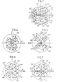
- FIGS. 3 to 7 show some modulation curves with directional arrows for the direction of passage, which have proven to be optimal under certain welding conditions.
- the different modulation curves have in common that with respect to the x-axis, i. H. the path curve tangent 12 and the welding joint of the workpiece mirror-symmetrical formation of the curve branches 40, which are traversed by the electron beam in mirror-image directions.
- the curve branches 40 both point 41 in their front x in the direction of movement also in its rear parts 42 a curve section 43 ', 43 "which is only slightly deflected in the normal direction y of the trajectory 12 and a curve section 45', 45" which is continuously connected to it via a deflection section 44 ', 44 " individual curve sections is selected such that the electron beam is moved at least in the curve sections 45 ′, 45 ′′ deflected more than the trajectory curve with a directional component corresponding to the direction of flow in the respectively adjacent regions of the melting zone 14.
- each modulation curve branch 40 the electron beam with a direction component pointing forward in the direction of movement and the more deflected curve portion 45 'with a direction component pointing backward pass through the little deflected curve section 43'.
- the optimal formation and direction of flow in the rear part 42 of the modulation curve depends on whether there is a laminar flow pattern or whether there is a vortex formation with the reversal of the direction of the flow pattern described above.
- the modulation curves shown in FIGS. 3 to 5 have proven their worth, the branches 40 of which in the rear part 42 in the more deflected curve section 45 "of the electron beam with a backward-pointing direction component and less deflected curve section 43 "with the directional component facing forward.
- FIGS. 6 and 7 since there in the rear part 42 of each curve branch 40 the less deflected curve section 43 "from Electron beam with backward-pointing direction component and the more deflected curve section 45 "with forward-facing direction component is traversed.
- the deflection paths 44 ′, 44 ′′ in the front and rear parts 41, 42 of the modulation curve branches 40 are outside the line of symmetry formed by the path curve tangent 12 in all exemplary embodiments This provides optimum support for the flow course with the least possible disturbance in the vicinity of the stagnation point on the front face 24 of the steam capillary 20.
- it can be expedient to further support the liquid flow as is the case in FIGS Separate parts 41, 42 of each deflection path 44 ′, 44 ′′ arranged in each modulation curve branch 40 by a constriction 46 directed towards the path curve 12.
- the path velocity of the electron beam on the modulation curve should at least be adapted to the flow conditions in the flow conditions in the melt and at least 1 to 10 times the flow velocity in the areas swept by the electron beam, at least in the course of its maximum deflection in the region of the deflection sections 44 ', 44 " the melting zone or 1 to 20 times the feed speed v of the workpiece 10.
- the modulation curve can also be traversed by the electron beam with a variable path speed.
- the electron beam is moved step by step along the discrete support points forming the modulation curve.
- the coordinates of the individual support points are read out sequentially from a digital memory arrangement, converted into analog current and voltage signals and in this form fed to the deflection coils or plates of an electron beam welding machine (FIG. 1).
- the electron beam can be moved continuously between two interpolation points on an interpolation path delimited by the interpolation points, wherein the interpolation points can have a variable distance from one another in order to generate a variable path speed.
- the diameter of the modulation curve should be a maximum of 5 times, preferably 2 to 4 times the half-width of the electron beam at the point of incidence.
- the electron beam in the course of the modulation curve is indicated in FIG. 3 in the form of small circles 47 with a diameter corresponding to the half-width.
Landscapes
- Engineering & Computer Science (AREA)
- Mechanical Engineering (AREA)
- Welding Or Cutting Using Electron Beams (AREA)
Claims (35)
Applications Claiming Priority (4)
| Application Number | Priority Date | Filing Date | Title |
|---|---|---|---|
| DE19823228846 DE3228846A1 (de) | 1982-08-02 | 1982-08-02 | Verfahren und anordnung zum bearbeiten eines werkstuecks mittels eines fokussierten elektronenstrahls |
| DE3228846 | 1982-08-02 | ||
| DE19823240887 DE3240887A1 (de) | 1982-11-05 | 1982-11-05 | Verfahren zum schweissen eines werkstuecks mittels eines fokussierten elektronenstrahls |
| DE3240887 | 1982-11-05 |
Publications (2)
| Publication Number | Publication Date |
|---|---|
| EP0100933A1 EP0100933A1 (fr) | 1984-02-22 |
| EP0100933B1 true EP0100933B1 (fr) | 1987-01-21 |
Family
ID=25803490
Family Applications (1)
| Application Number | Title | Priority Date | Filing Date |
|---|---|---|---|
| EP83107091A Expired EP0100933B1 (fr) | 1982-08-02 | 1983-07-20 | Méthode et dispositif pour le traitement d'une pièce d'usinage par un rayon électronique focalisé |
Country Status (3)
| Country | Link |
|---|---|
| US (1) | US4591688A (fr) |
| EP (1) | EP0100933B1 (fr) |
| DE (1) | DE3369264D1 (fr) |
Families Citing this family (14)
| Publication number | Priority date | Publication date | Assignee | Title |
|---|---|---|---|---|
| US5603853A (en) * | 1995-02-28 | 1997-02-18 | The Twentyfirst Century Corporation | Method of high energy density radiation beam lap welding |
| US5595670A (en) * | 1995-04-17 | 1997-01-21 | The Twentyfirst Century Corporation | Method of high speed high power welding |
| US6110318A (en) * | 1997-11-26 | 2000-08-29 | Science Research Laboratory | System for selective electron beam irradiation |
| US20060102597A1 (en) * | 2004-11-16 | 2006-05-18 | Exponent, Inc. | Electron beam welding method and apparatus using controlled volumetric heating |
| US8253062B2 (en) * | 2005-06-10 | 2012-08-28 | Chrysler Group Llc | System and methodology for zero-gap welding |
| US7876906B2 (en) * | 2006-05-30 | 2011-01-25 | Sonitus Medical, Inc. | Methods and apparatus for processing audio signals |
| US8803029B2 (en) * | 2006-08-03 | 2014-08-12 | Chrysler Group Llc | Dual beam laser welding head |
| US8198565B2 (en) * | 2007-04-11 | 2012-06-12 | Chrysler Group Llc | Laser-welding apparatus and method |
| US9358635B2 (en) * | 2013-12-19 | 2016-06-07 | Siemens Energy, Inc. | Rastered laser melting of a curved surface path with uniform power density distribution |
| EP3012057B1 (fr) * | 2014-10-24 | 2019-04-24 | General Electric Technology GmbH | Procédé de soudage de joints profonds |
| WO2016103493A1 (fr) * | 2014-12-26 | 2016-06-30 | 技術研究組合次世代3D積層造形技術総合開発機構 | Dispositif d'impression 3d, procédé de commande de dispositif d'impression 3d et programme de commande |
| ES2887211T3 (es) * | 2015-06-19 | 2021-12-22 | Ipg Photonics Corp | Sistema de soldadura láser con un cabezal de soldadura láser dotado de espejos móviles duales que proporcionan movimiento de haz con campo de visión limitado |
| EP3223299A4 (fr) * | 2016-01-21 | 2018-04-18 | Technology Research Association for Future Additive Manufacturing | Dispositif de modélisation 3d, procédé de commande de dispositif de modélisation 3d et programme de commande de dispositif de modélisation 3d |
| SE2450809A1 (en) * | 2024-07-12 | 2025-04-10 | Freemelt Ab | Methods and arrangements for controlling fusion parameters in additive manufacturing |
Family Cites Families (3)
| Publication number | Priority date | Publication date | Assignee | Title |
|---|---|---|---|---|
| US4179316A (en) * | 1977-10-17 | 1979-12-18 | Sciaky Bros., Inc. | Method and apparatus for heat treating |
| DE3043635C1 (de) * | 1980-11-19 | 1987-05-07 | Institut für Kerntechnik und Energiewandlung e.V., 7000 Stuttgart | Verfahren und Anordnung zum automatischen Elektronenstrahlschweißen |
| US4376886A (en) * | 1981-01-02 | 1983-03-15 | Sciaky Bros., Inc. | Method for electron beam welding |
-
1983
- 1983-07-20 EP EP83107091A patent/EP0100933B1/fr not_active Expired
- 1983-07-20 DE DE8383107091T patent/DE3369264D1/de not_active Expired
- 1983-07-29 US US06/518,351 patent/US4591688A/en not_active Expired - Lifetime
Also Published As
| Publication number | Publication date |
|---|---|
| DE3369264D1 (en) | 1987-02-26 |
| EP0100933A1 (fr) | 1984-02-22 |
| US4591688A (en) | 1986-05-27 |
Similar Documents
| Publication | Publication Date | Title |
|---|---|---|
| EP0100933B1 (fr) | Méthode et dispositif pour le traitement d'une pièce d'usinage par un rayon électronique focalisé | |
| DE102019210019B4 (de) | Optische Apparatur zum Laserschweißen eines Werkstücks, Verfahren zum Laserschweißen eines Werkstücks mittels mehrerer Teilstrahlen sowie Verwendung einer optischen Apparatur zum Laserschweißen | |
| EP3256285B1 (fr) | Dispositif d'irradiation, machine de traitement et procédé de fabrication d'une couche ou d'une sous-zone d'une couche d'une pièce tridimensionnelle | |
| EP0135851A2 (fr) | Procédé et dispositif pour marquer des pièces de travail, notamment des éléments de construction électroniques | |
| EP3414044B1 (fr) | Procédé de production d'une partie d'une couche d'un composant tridimensionnel | |
| DE102014210486A1 (de) | Verfahren und Vorrichtung zum Verschweißen zweier Fügepartner aus thermoplastischen Kunststoffen entlang einer Schweißnaht mittels Laser | |
| EP2747984A1 (fr) | Procédé et dispositif pour le soudage au laser de deux parties en matière plastique à assembler | |
| DE102009044316A1 (de) | Laserbearbeitungsvorrichtung und Verfahren zur Herstellung einer Fläche an einem Rohling | |
| DE102007063456A1 (de) | Verfahren zum Schweißverbinden von Werkstücken aus einem metallischen Werkstoff mit einem Laserstrahl | |
| DE102018125731A1 (de) | Verfahren und Vorrichtung zum Herstellen eines dreidimensionalen Werkstücks | |
| DE1053691B (de) | Verfahren und Einrichtung zur Materialbearbeitung mittels Ladungstraegerstrahl | |
| DE102007038502A1 (de) | Verfahren zum Fügen von mindestens zwei Bauteilen mittels Laserstrahlung | |
| EP3743261B1 (fr) | Procédé et dispositif permettant d'améliorer la qualité de construction d'objets fabriqués par un procédé de fabrication additive | |
| WO2022078625A1 (fr) | Appareil de soudage comportant un dispositif de buses pour refroidir une pièce pendant le processus de soudage | |
| DE2634341A1 (de) | Verfahren und einrichtung zum ausrichten eines ladungstraegerstrahles eines technischen ladungstraegerstrahlgeraetes | |
| EP1479506B1 (fr) | Procédé de soudage pour des plastiques structurés | |
| DE2821028A1 (de) | Verfahren und einrichtung zur strahlpositionsregelung in einem ladungstraegerstrahlgeraet | |
| DE102019219276A1 (de) | Hatchumkehr mit Keyhole-Übergabe | |
| DE102018127649B4 (de) | Verfahren zum Laserschweißen mit stabilem Schmelzbad und Laserbearbeitungsvorrichtung | |
| DE112021003368T5 (de) | Laserschweissverfahren und laserschweissvorrichtung | |
| EP0266764A2 (fr) | Méthode et dispositif de guidage d'un rayon laser de puissance le long d'un joint | |
| DE1765852C3 (de) | Vorrichtung zur Bearbeitung von Werkstoffen mit magnetisch fokussierten Ladungsträgerstrahlen | |
| EP0889769B1 (fr) | Procede pour assembler des pieces au moyen d'un faisceau laser | |
| DE2204295A1 (de) | Verfahren und Vorrichtung zum Schweißen mit Elektronenstrahlen bei höheren Geschwindigkeiten | |
| DE3843841A1 (de) | Laserstrahlschweissverfahren |
Legal Events
| Date | Code | Title | Description |
|---|---|---|---|
| PUAI | Public reference made under article 153(3) epc to a published international application that has entered the european phase |
Free format text: ORIGINAL CODE: 0009012 |
|
| AK | Designated contracting states |
Designated state(s): DE FR GB |
|
| 17P | Request for examination filed |
Effective date: 19840526 |
|
| GRAA | (expected) grant |
Free format text: ORIGINAL CODE: 0009210 |
|
| AK | Designated contracting states |
Kind code of ref document: B1 Designated state(s): DE FR GB |
|
| REF | Corresponds to: |
Ref document number: 3369264 Country of ref document: DE Date of ref document: 19870226 |
|
| ET | Fr: translation filed | ||
| PLBI | Opposition filed |
Free format text: ORIGINAL CODE: 0009260 |
|
| 26 | Opposition filed |
Opponent name: MESSER GRIESHEIM GMBH Effective date: 19871021 |
|
| PLBN | Opposition rejected |
Free format text: ORIGINAL CODE: 0009273 |
|
| STAA | Information on the status of an ep patent application or granted ep patent |
Free format text: STATUS: OPPOSITION REJECTED |
|
| 27O | Opposition rejected |
Effective date: 19880915 |
|
| PGFP | Annual fee paid to national office [announced via postgrant information from national office to epo] |
Ref country code: FR Payment date: 19980810 Year of fee payment: 16 |
|
| PGFP | Annual fee paid to national office [announced via postgrant information from national office to epo] |
Ref country code: GB Payment date: 19980819 Year of fee payment: 16 |
|
| PG25 | Lapsed in a contracting state [announced via postgrant information from national office to epo] |
Ref country code: GB Free format text: LAPSE BECAUSE OF NON-PAYMENT OF DUE FEES Effective date: 19990720 |
|
| PG25 | Lapsed in a contracting state [announced via postgrant information from national office to epo] |
Ref country code: FR Free format text: THE PATENT HAS BEEN ANNULLED BY A DECISION OF A NATIONAL AUTHORITY Effective date: 19990731 |
|
| GBPC | Gb: european patent ceased through non-payment of renewal fee |
Effective date: 19990720 |
|
| REG | Reference to a national code |
Ref country code: FR Ref legal event code: ST |
|
| PGFP | Annual fee paid to national office [announced via postgrant information from national office to epo] |
Ref country code: DE Payment date: 20020829 Year of fee payment: 20 |