EP0100997A2 - Dispositif électronique fonctionnant avec des ondes acoustiques réfléchies - Google Patents
Dispositif électronique fonctionnant avec des ondes acoustiques réfléchies Download PDFInfo
- Publication number
- EP0100997A2 EP0100997A2 EP83107618A EP83107618A EP0100997A2 EP 0100997 A2 EP0100997 A2 EP 0100997A2 EP 83107618 A EP83107618 A EP 83107618A EP 83107618 A EP83107618 A EP 83107618A EP 0100997 A2 EP0100997 A2 EP 0100997A2
- Authority
- EP
- European Patent Office
- Prior art keywords
- finger
- fingers
- weighting
- wave propagation
- main wave
- Prior art date
- Legal status (The legal status is an assumption and is not a legal conclusion. Google has not performed a legal analysis and makes no representation as to the accuracy of the status listed.)
- Granted
Links
- 239000006185 dispersion Substances 0.000 description 5
- 238000006073 displacement reaction Methods 0.000 description 4
- 230000005540 biological transmission Effects 0.000 description 2
- 230000000694 effects Effects 0.000 description 2
- 239000000758 substrate Substances 0.000 description 2
- 230000001419 dependent effect Effects 0.000 description 1
- 238000011161 development Methods 0.000 description 1
- 230000018109 developmental process Effects 0.000 description 1
- 238000004519 manufacturing process Methods 0.000 description 1
- 239000000463 material Substances 0.000 description 1
- 238000001465 metallisation Methods 0.000 description 1
Images
Classifications
-
- H—ELECTRICITY
- H03—ELECTRONIC CIRCUITRY
- H03H—IMPEDANCE NETWORKS, e.g. RESONANT CIRCUITS; RESONATORS
- H03H9/00—Networks comprising electromechanical or electro-acoustic elements; Electromechanical resonators
- H03H9/46—Filters
- H03H9/64—Filters using surface acoustic waves
- H03H9/6423—Means for obtaining a particular transfer characteristic
- H03H9/643—Means for obtaining a particular transfer characteristic the transfer characteristic being determined by reflective or coupling array characteristics
Definitions
- the present invention relates to an electronic component as specified in the preamble of claim 1.
- German patent applications P 31 21 516.5 (81 P 7048), P 32 09 948.7 (82 P 1190) and P 32 09 962.2 (82 P 1191) describe a surface wave filter in the manner of a dispersive delay line and an improvement to such a filter .
- it is an electronic component working with acoustic waves, in which the finger weighting provided to achieve a certain predetermined transfer function is realized in that the distances of finger groups from one another and in particular individual fingers from one another such a position of the fingers is changed, which would correspond to such a component without finger weighting.
- this finger weighting is realized by the principle according to finger length weighting known per se and the non-equidistant distances of fingers or finger groups from one another provided for this component serve to achieve a predetermined dispersion of this component.
- the invention of the application P 32 09 962.2 offers the advantage (apart from a dispersion realized in this component) that for the given amplitudes Function of the transfer characteristic necessary finger weighting so that the active portions of the individual fingers of the digital structure (s) used in each case over the entire width of the working area of this electronic component, that is over the entire width of the structure (s) transverse to the main direction of propagation of the extend acoustic wave.
- finger weighting which are associated with finger length-weighted structures or with finger dot-weighted structures.
- the necessary finger weighting (based on a non-weighted structure) can be shifted between adjacent fingers, i.e. a respective group of fingers to be subjected to finger weighting consists of only two Fingers. Maximum bandwidth is thus achieved for a structure or for a component according to this older invention.
- the present invention is based on the consideration that, compared to the older invention, an even greater bandwidth of the respective digital structure or of the entire component can only be achieved by taking a comparatively different approach.
- this approach it is possible to start from a known electronic component working with acoustic waves and, for example, also from a component of the earlier application P 31 21 516, which has varied finger spacings for the realization of a dispersion.
- the present invention is based on the idea of performing a “finger shift” in such a way that it already acts as a finger weighting on or in the individual finger.
- the solution principle on which this is based is to subdivide the respective individual finger to be subjected to finger weighting of a relevant structure of the electronic component in its longitudinal direction at least once and to arrange the at least two resulting parts offset relative to one another parallel to the main wave propagation direction.
- the main wave propagation direction is the direction in which the acoustic wave is intended to run in the electronic component. In the case of a component with 180 ° reflection, this is usually a single direction.
- a main wave propagation direction which is traversed in the direction of execution and parallel to it in the back direction and a further main direction.
- Wave propagation direction that is transverse to it.
- the displacement of the finger parts can be parallel to one main wave propagation direction or to the other main wave propagation direction or else partly to one and partly to the other main wave propagation direction.
- the longitudinal direction mentioned in connection with the division of the individual fingers is the direction of the largest geometric dimension of the individual fingers. In a component with 180 ° reflection, this longitudinal direction of the fingers is generally orthogonal to the main wave propagation direction.
- this longitudinal direction of the fingers concerned for example with 90 ° reflection in the component, generally runs at an angle of 45 ° to one and the other main wave propagation direction (assumed homogeneous or isotropic conditions).
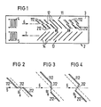
- FIG. 1 shows a basic embodiment of an electronic component working with reflected acoustic waves with wave reflection at an angle other than 180 °.
- the structures shown or the existing electrode fingers are preferably metallization strips which are located on the upper surface 3 of the substrate body 2 in FIG. 1.
- 4 and 5 designate two interdigital transducer structures known per se.
- an acoustic surface wave is generated in the piezoelectric material of the surface 3 of the substrate body 2 from the electrical input signal.
- an electrical signal can be recovered from the received acoustic wave.
- Electrical input signal and output signal differ according to the transfer function specified for this element.
- the converter 4 is assumed as the input and the converter 5 as the output, so that main wave propagation directions result, which are indicated by the arrows 6, 7 and 8.
- the acoustic wave thus running in the direction of arrow 6 strikes a first reflection digital structure 11, which consists of a plurality of reflection fingers 12 inclined in a manner known per se. After the reflection in the direction of arrow 8 on these fingers 12, the acoustic wave strikes the illustrated second reflection digital structure, which consists of a plurality of again inclined reflector fingers 14. After reflection on this structure 13, the wave runs or the main wave propagation direction is parallel to the direction of arrow 7.
- the respective length of a reflection digital structure 11, 13 depends in a manner known per se on the given requirements that are placed on the electronic component in question.
- the reflection digital structure 11 contains a finger weighting with which the predetermined transfer function of the component is fulfilled with regard to the amplitude function.
- any necessary dispersion property can be achieved by non-equidistant distances between individual fingers or groups of fingers with respect to one another, the distances referred to in this regard relating to a position of the individual fingers of a digital structure that does not involve any dispersion (and also no finger weighting due to finger displacement) according to the older invention).
- such a non-dispersive, non-weighted reflection digital structure is shown with the structure 13.
- structure 13 is also dispersive and / or weighted eigen shaft could be given against each other by transverse displacement.
- those electrode fingers 12 that must have an appropriate weighting are subdivided once in their length, so that two partial fingers 112, 212 each result. These two partial fingers are shifted against each other by the amount resulting from the required weighting, and in FIG. 1 parallel to the main wave propagation direction 6. As is customary for finger weighting, this finger weighting is distributed over the entire (finger-weighted) reflection in the manner of a modulation -Digital structure 11. For a displacement of the partial fingers 112 and 212 against one another by the dimension A / 2, a finger weighting of a zero results (which would correspond to an overlap 'zero' if the overlap weighting was known).
- An offset of the two finger parts 112 and 212 in the size 'zero' corresponds to a transmission maximum (or complete overlapping).
- Intermediate values of the offset of the finger parts 112, 212 relative to one another result in the corresponding intermediate values of finger weighting between the transmission maximum and minimum due to less strong interference.
- the component parallel to the relevant main wave propagation direction here direction of arrow 6 is decisive for the offset. In the exemplary embodiment in FIG. 1, because of the inclined position of the fingers 12, this is the projection onto the direction of the arrow 6.
- Figures 2, 3 and 4 show side by side for a finger (for example for a finger 12) of a component with an oblique reflection digital structure three possibilities of the finger weighting offset according to the invention, namely Figure 2 (as already in Figure 1) the offset parallel to the direction arrow 6, Fi 3 the offset (alone) in the direction parallel to the direction of arrow 8 and FIG. 4 an offset partially parallel to the direction of arrow 6 (or 7) and partially parallel to the direction of arrow 8.
- the measure corresponding to FIG. 2 is suitably conceivable
- FIGS. 2 to 4 it should be pointed out that they are substantially enlarged sections compared to the magnitude of FIG. 1.
- the other reflection digital structure 13 can also have the finger weighting according to the invention (instead of the reflection digital structure 12 (described above for structure 11).
- the necessary finger weighting can also be distributed over both reflection digital structures 11, 13 can be achieved, for example, that the necessary finger offset is divided accordingly smaller.
- the length of an individual finger can also be divided into more than just two finger parts 112, 212.
- a multiple subdivision of each finger in the longitudinal direction allows a refinement of the structure in question, but with the corresponding additional technological effort.
- the partial fingers 112, 212 belonging to a finger 12 can be connected to one another (312), as indicated by dashed lines in FIGS. 2 to 4. Interference caused by such a connection 312 is generally negligible, since the respective distances between the adjacent ends of the respective partial fingers 112, 212 or the lengths of the individual connections are one or more sizes Arrangements are smaller than the length of the fingers 12 or partial fingers 112, 212. Technological advantages for the production of the structure can thus be achieved.
Landscapes
- Physics & Mathematics (AREA)
- Acoustics & Sound (AREA)
- Surface Acoustic Wave Elements And Circuit Networks Thereof (AREA)
Applications Claiming Priority (2)
| Application Number | Priority Date | Filing Date | Title |
|---|---|---|---|
| DE3230038 | 1982-08-12 | ||
| DE19823230038 DE3230038A1 (de) | 1982-08-12 | 1982-08-12 | Mit reflektierten akustischen wellen arbeitendes elektronisches bauelement |
Publications (3)
| Publication Number | Publication Date |
|---|---|
| EP0100997A2 true EP0100997A2 (fr) | 1984-02-22 |
| EP0100997A3 EP0100997A3 (en) | 1985-10-16 |
| EP0100997B1 EP0100997B1 (fr) | 1989-02-01 |
Family
ID=6170711
Family Applications (1)
| Application Number | Title | Priority Date | Filing Date |
|---|---|---|---|
| EP83107618A Expired EP0100997B1 (fr) | 1982-08-12 | 1983-08-02 | Dispositif électronique fonctionnant avec des ondes acoustiques réfléchies |
Country Status (4)
| Country | Link |
|---|---|
| US (1) | US4520330A (fr) |
| EP (1) | EP0100997B1 (fr) |
| JP (1) | JPS5950608A (fr) |
| DE (2) | DE3230038A1 (fr) |
Cited By (1)
| Publication number | Priority date | Publication date | Assignee | Title |
|---|---|---|---|---|
| EP0151275A3 (en) * | 1984-02-09 | 1985-12-27 | Siemens Aktiengesellschaft | Electronic device for reflected surface acoustic waves |
Families Citing this family (8)
| Publication number | Priority date | Publication date | Assignee | Title |
|---|---|---|---|---|
| DE3731309A1 (de) * | 1987-09-17 | 1989-03-30 | Siemens Ag | Oberflaechenwellenanordnung mit konversionsstruktur zur vermeidung unerwuenschter reflektierter wellen |
| EP0571365B1 (fr) * | 1989-11-14 | 1994-10-26 | Siemens Aktiengesellschaft | Filtre reflecteur d'ondes de surface |
| DE4018784A1 (de) * | 1990-06-12 | 1991-12-19 | Siemens Ag | Oberflaechenwellen-reflektorfilter |
| DE3937871A1 (de) * | 1989-11-14 | 1991-05-16 | Siemens Ag | Oberflaechenwellen-reflektorfilter |
| DE3942148A1 (de) * | 1989-12-20 | 1991-06-27 | Siemens Ag | Oberflaechenwellen-reflektorfilter |
| DE3942140A1 (de) * | 1989-12-20 | 1991-06-27 | Siemens Ag | Oberflaechenwellen-reflektorfilter |
| ES2036950B1 (es) * | 1991-11-28 | 1996-02-16 | Alcatel Standard Electrica | Filtro de ondas acusticas superficiales resonante de bajas perdidas utilizando acoplador-reflector multistrip |
| DE4213117A1 (de) * | 1992-04-21 | 1993-10-28 | Siemens Ag | Gewichtete Reflektorstruktur für Oberflächenwellenanordnungen |
Family Cites Families (10)
| Publication number | Priority date | Publication date | Assignee | Title |
|---|---|---|---|---|
| GB1492987A (en) * | 1974-07-02 | 1977-11-23 | Secr Defence | Surface acoustic wave devices |
| JPS583414B2 (ja) * | 1978-02-03 | 1983-01-21 | クラリオン株式会社 | 表面弾性波フィルタ |
| US4327340A (en) * | 1978-09-19 | 1982-04-27 | Bell Telephone Laboratories Incorporated | Surface wave resonator cascade |
| GB2030411B (en) * | 1978-09-25 | 1982-12-08 | Plessey Co Ltd | Surface acoustic wave filters |
| FR2466139B1 (fr) * | 1979-09-20 | 1988-03-04 | Nat Res Dev | Dispositif reflecteur d'ondes acoustiques superficielles |
| JPS5672516A (en) * | 1979-11-16 | 1981-06-16 | Seiko Epson Corp | Elastic surface wave filter |
| US4267534A (en) * | 1980-05-23 | 1981-05-12 | Sperry Corporation | Surface acoustic wave reflectors with weighted arrays of segmented and non-segmented lineal elements |
| DE3121516A1 (de) * | 1981-05-29 | 1983-01-05 | Siemens AG, 1000 Berlin und 8000 München | Pulskompressionsfilter nach art einer dispersiven verzoegerungsleitung |
| DE3209948A1 (de) * | 1982-03-18 | 1983-09-22 | Siemens AG, 1000 Berlin und 8000 München | Verbesserung an einem pulskompressionsfilter nach art einer dispersiven verzoegerungsleitung |
| DE3209962A1 (de) * | 1982-03-18 | 1983-09-29 | Siemens AG, 1000 Berlin und 8000 München | Mit akustischen wellen arbeitendes elektronisches bauelement |
-
1982
- 1982-08-12 DE DE19823230038 patent/DE3230038A1/de not_active Withdrawn
-
1983
- 1983-08-02 EP EP83107618A patent/EP0100997B1/fr not_active Expired
- 1983-08-02 DE DE8383107618T patent/DE3379143D1/de not_active Expired
- 1983-08-04 US US06/520,418 patent/US4520330A/en not_active Expired - Lifetime
- 1983-08-08 JP JP58144848A patent/JPS5950608A/ja active Pending
Cited By (1)
| Publication number | Priority date | Publication date | Assignee | Title |
|---|---|---|---|---|
| EP0151275A3 (en) * | 1984-02-09 | 1985-12-27 | Siemens Aktiengesellschaft | Electronic device for reflected surface acoustic waves |
Also Published As
| Publication number | Publication date |
|---|---|
| DE3230038A1 (de) | 1984-02-16 |
| EP0100997B1 (fr) | 1989-02-01 |
| EP0100997A3 (en) | 1985-10-16 |
| DE3379143D1 (en) | 1989-03-09 |
| US4520330A (en) | 1985-05-28 |
| JPS5950608A (ja) | 1984-03-23 |
Similar Documents
| Publication | Publication Date | Title |
|---|---|---|
| EP0089617B1 (fr) | Elément de circuit électronique à ondes acoustiques de surface | |
| DE2016109C3 (de) | Filter nach dem Oberflächenwellenprinzip | |
| DE2848267C3 (de) | Akustische Oberflachenwelleneinrichtung | |
| DE69100625T2 (de) | Akustische oberflächenwellenfilter. | |
| DE3025871C2 (de) | Akustische Oberflächenwelleneinrichtung | |
| DE2437938C3 (de) | Oberflächenschallwellenvorrichtung | |
| DE2739688C2 (fr) | ||
| EP0100997A2 (fr) | Dispositif électronique fonctionnant avec des ondes acoustiques réfléchies | |
| DE2431193A1 (de) | Mit akustischen oberflaechenwellen arbeitende anordnung | |
| DE3301109A1 (de) | Dispersive akustische oberflaechenwellen-verzoegerungsleitung | |
| DE2826891C3 (de) | Elastizitätsoberflächenwellen-Bauelement | |
| EP0101077B1 (fr) | Dispositif électronique à ondes acoustiques réfléchies | |
| EP0124019B1 (fr) | Filtre-résonateur à ondes acoustiques de surface | |
| DE2839851C2 (de) | Oberflächenwellenanordnung mit verbesserter Störsignalunterdrückung | |
| DE2618210C3 (de) | Wandlerelektroden für Filter oder Verzögerungsleitungen nach dem Oberflächenwellenprinzip | |
| DE3529916A1 (de) | Dispersiver interdigital-wandler fuer mit akustischen wellen arbeitenden anordnungen | |
| DE68902810T2 (de) | Wandler fuer ein akustisches oberflaechenwellen-filter. | |
| DE2139200B2 (de) | Umsetzer zur Erzeugung und Wiedergabe von binären Impulsfolgen in Form von Oberflächenwellen | |
| EP0436556A1 (fr) | Filtre a ondes de surface. | |
| DE2835107C3 (de) | Wandlerelektrodenanordnung für einen elektromechanischen Wandler nach dem Oberflächenwellenprinzip | |
| EP0151275B1 (fr) | Dispositif électronique pour des ondes acoustiques de surface réfléchies | |
| EP0088400A2 (fr) | Transducteur interdigital avec suppression de signaux de brouillage réfléchis | |
| DE8222799U1 (de) | Mit reflektierten akustischen Wellen arbeitendes elektronisches Bauelement | |
| DE2854072A1 (de) | Akustische oberflaechenwellenanordnung | |
| DE2618144C3 (de) | Wandlerelektroden für Filter oder Verzögerungsleitungen nach dem Oberflächenwellenprinzip |
Legal Events
| Date | Code | Title | Description |
|---|---|---|---|
| PUAI | Public reference made under article 153(3) epc to a published international application that has entered the european phase |
Free format text: ORIGINAL CODE: 0009012 |
|
| AK | Designated contracting states |
Designated state(s): DE FR GB |
|
| 17P | Request for examination filed |
Effective date: 19841112 |
|
| PUAL | Search report despatched |
Free format text: ORIGINAL CODE: 0009013 |
|
| AK | Designated contracting states |
Designated state(s): DE FR GB |
|
| 17Q | First examination report despatched |
Effective date: 19871202 |
|
| GRAA | (expected) grant |
Free format text: ORIGINAL CODE: 0009210 |
|
| AK | Designated contracting states |
Kind code of ref document: B1 Designated state(s): DE FR GB |
|
| REF | Corresponds to: |
Ref document number: 3379143 Country of ref document: DE Date of ref document: 19890309 |
|
| ET | Fr: translation filed | ||
| GBT | Gb: translation of ep patent filed (gb section 77(6)(a)/1977) | ||
| PLBE | No opposition filed within time limit |
Free format text: ORIGINAL CODE: 0009261 |
|
| STAA | Information on the status of an ep patent application or granted ep patent |
Free format text: STATUS: NO OPPOSITION FILED WITHIN TIME LIMIT |
|
| 26N | No opposition filed | ||
| REG | Reference to a national code |
Ref country code: FR Ref legal event code: TP |
|
| REG | Reference to a national code |
Ref country code: GB Ref legal event code: IF02 |
|
| PGFP | Annual fee paid to national office [announced via postgrant information from national office to epo] |
Ref country code: FR Payment date: 20020717 Year of fee payment: 20 |
|
| PGFP | Annual fee paid to national office [announced via postgrant information from national office to epo] |
Ref country code: GB Payment date: 20020724 Year of fee payment: 20 |
|
| PGFP | Annual fee paid to national office [announced via postgrant information from national office to epo] |
Ref country code: DE Payment date: 20020830 Year of fee payment: 20 |
|
| PG25 | Lapsed in a contracting state [announced via postgrant information from national office to epo] |
Ref country code: GB Free format text: LAPSE BECAUSE OF EXPIRATION OF PROTECTION Effective date: 20030801 |
|
| REG | Reference to a national code |
Ref country code: GB Ref legal event code: PE20 |