EP0101528B1 - Analoge Zweidrahtübertragungssysteme - Google Patents
Analoge Zweidrahtübertragungssysteme Download PDFInfo
- Publication number
- EP0101528B1 EP0101528B1 EP82304374A EP82304374A EP0101528B1 EP 0101528 B1 EP0101528 B1 EP 0101528B1 EP 82304374 A EP82304374 A EP 82304374A EP 82304374 A EP82304374 A EP 82304374A EP 0101528 B1 EP0101528 B1 EP 0101528B1
- Authority
- EP
- European Patent Office
- Prior art keywords
- transmitter
- current
- supply lines
- communication
- digital
- Prior art date
- Legal status (The legal status is an assumption and is not a legal conclusion. Google has not performed a legal analysis and makes no representation as to the accuracy of the status listed.)
- Expired
Links
- 238000004891 communication Methods 0.000 title claims description 34
- 230000005540 biological transmission Effects 0.000 claims description 14
- 230000008859 change Effects 0.000 claims description 5
- 238000000034 method Methods 0.000 description 14
- 230000008569 process Effects 0.000 description 12
- 239000003990 capacitor Substances 0.000 description 4
- 230000011664 signaling Effects 0.000 description 4
- 238000010586 diagram Methods 0.000 description 3
- 230000000977 initiatory effect Effects 0.000 description 2
- 238000010276 construction Methods 0.000 description 1
- 230000008878 coupling Effects 0.000 description 1
- 238000010168 coupling process Methods 0.000 description 1
- 238000005859 coupling reaction Methods 0.000 description 1
- 230000005669 field effect Effects 0.000 description 1
- 230000004044 response Effects 0.000 description 1
- 230000008054 signal transmission Effects 0.000 description 1
- 230000007704 transition Effects 0.000 description 1
Images

Classifications
-
- H—ELECTRICITY
- H04—ELECTRIC COMMUNICATION TECHNIQUE
- H04B—TRANSMISSION
- H04B3/00—Line transmission systems
- H04B3/54—Systems for transmission via power distribution lines
- H04B3/548—Systems for transmission via power distribution lines the power on the line being DC
-
- G—PHYSICS
- G08—SIGNALLING
- G08C—TRANSMISSION SYSTEMS FOR MEASURED VALUES, CONTROL OR SIMILAR SIGNALS
- G08C19/00—Electric signal transmission systems
- G08C19/02—Electric signal transmission systems in which the signal transmitted is magnitude of current or voltage
-
- H—ELECTRICITY
- H04—ELECTRIC COMMUNICATION TECHNIQUE
- H04B—TRANSMISSION
- H04B2203/00—Indexing scheme relating to line transmission systems
- H04B2203/54—Aspects of powerline communications not already covered by H04B3/54 and its subgroups
- H04B2203/5462—Systems for power line communications
- H04B2203/547—Systems for power line communications via DC power distribution
-
- H—ELECTRICITY
- H04—ELECTRIC COMMUNICATION TECHNIQUE
- H04B—TRANSMISSION
- H04B2203/00—Indexing scheme relating to line transmission systems
- H04B2203/54—Aspects of powerline communications not already covered by H04B3/54 and its subgroups
- H04B2203/5462—Systems for power line communications
- H04B2203/5483—Systems for power line communications using coupling circuits
Definitions
- the present invention is related to data communication systems, and more specifically to analog systems of the 2-wire type utilizing power supply circuits.
- 2-wire analog transmission systems are well known.
- One standard form of such systems utilizes a power supply coupled to a transmitter via a resistor, with the transmitter sensing some condition and signalling the value of the sensed condition by controlling the current drawn from the power supply between 4 and 20 ma, see for example Advances in Instrumentation, vol. 29, No. 4, 1974, pages 1 to 5.
- the 4 ma minimum current is sufficient to energize the circuitry of the transmitter, and the excess of current drawn, above the 4 ma level, indicates the value of the condition.
- This system has the limitation that its accuracy is limited to at best around 0.1 %, and is essentially a unidirectional system with the transmitter being essentially uncontrolled and transmitting continuously. While such systems are well established, they are therefore limited in both accuracy and function. Furthermore, although microprocessor techniques are being utilized in the construction of transmitters, only very limited advantages can be taken of the facilities which such techniques permit, because of the analog and unidirectional nature of the transmitters in the system.
- the object of the present invention is to provide a simple yet effective expansion of such systems to permit digital as well as analog signalling.
- the present invention provides a data communication system comprising:
- means for sensing the current flowing in the supply lines characterized by a communication device, coupled to the supply lines, which can generate a digital sequence of signal pulses represented by two different current levels drawn from the supply lines;
- the transmitter being responsive to the first such pulse to terminate its analog output and receive the subsequent pulses.
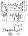
- a power supply 4 is coupled to a transmitter 2 via a pair of lines 17, one of which includes a resistor RO of at least 250 ⁇ .
- the transmitter 2 draws a current of between 4 and 20 mA, in dependence on a sensed condition (commonly called the process variable, PV).
- the transmitter signal may be sensed, for example, by an analog-to-digital converter 70 coupled across the resistor RO and feeding a display unit 74.
- the power supply 4 of course, produces a constant voltage, so that the current transmitted by the transmitter 2 is converted to a corresponding voltage across resistor RO.
- the wires 17 have a communication device 8 coupled to them.
- This device may for example be a hand-held device, somewhat like a pocket calculator, with a keyboard and display, which can be plugged onto the wires 17 at any convenient point.
- the normal steady or slowly varying process variable signal is effectively interrupted, and digital signalling occurs, using the two signal levels of 4 to 20 mA. Two directions of signalling have to be considered; from the communication device 8 to the transmitter 2, and vice versa.
- the device 8 accepts or "sinks" 16 mA from the line pair 17 for a binary 1 and 0 mA for a binary 0.
- the transmitter 2 senses this current variation as a voltage change across its input/output terminals. This voltage change occurs because the 16 mA drawn by the device 8 for a 0 causes an additional 4 V voltage drop across the resistor RO, and this 4 V change appears at the input to transmitter 2.
- the transmitter 2 responds only to voltage variations substantially more rapid than those allowed in analog signal transmission. Thus the transmitter 2 can send both analog and digital signals but receives only digital signals.
- FIG. 4A shows waveforms for a data transmission initiated by the device 8.
- the main waveform is the total current through the resistor RO, i.e. the combined currents drawn by the transmitter 2 and the device 8.
- the process variable (PV) current can be anywhere in the range of 4 to 20 mA.
- the communication device draws an additional 16 mA from the loop making the total loop current 20 to 36 mA. This occurs for only one digital bit time and is used as a "signal initiation" bit S to signal to the transmitter 2 that communication is being initiated.
- the voltage at the transmitter input terminal will drop by 4 V.
- the transmitter 2 When the transmitter 2 senses the drop in voltage at its input/output terminals, it waits for one bit time and then drops its own current drain from the former process variable level to a new level of 4 mA. This current drop is matched by a concurrent drop in current drain by the communication device 8 from 16 to 0 mA. Total loop current then drops from the range of 20 to 36 mA down to 4 mA, giving a 0 bit. The transmitter 2 maintains its current drain of 4 mA until the communication operation is finished. The loop current is then set for each bit, including the "start" bit 1 and any parity bits, to 4 or 20 mA by the communication device 8.
- the communication format shown in Figure 4A comprises the transmission of 2 bytes B1 and B2 of 8 bits each. Each byte is preceded by a 0 bit for reference and a 1 start bit. The 0 level following the second byte B2 lasts for the time t, as shown.
- Figure 4B shows waveforms for a digital data transmission initiated by the (PV) transmitter 2 to the device 8.
- the transmitter 2 forces its current drain to increase from the process variable level (4 to 20 mA) to 20 ma. It holds this current level for one bit time as a "signal initiate” bit S, then drops the current level to 4 mA. This 0 is also held for one bit time, after which the information transmission starts with a "start" bit 1.
- Digital transmission from the transmitter 2 to the device 8 continues with the loop current being varied by the transmitter 2 between 4 and 20 mA for each bit until the communication operation is completed.
- Completion of the communication operation occurs when the loop current is held steady at 4 mA for the predefined time period t, after which the transmitter 2 adjusts the loop current back to the former process variable level in the range of 4 to 20 mA.
- Figure 4B shows the transmission of a single 8-bit byte B1.
- FIG. 2 shows the communication device 8 in more detail.
- the device consists of 3 main sections: a communications controller, a current driver 26, and a current receiver 24.
- the communications controller section includes a microprocessor CPU 10 coupled to a keyboard 40 and a universal asynchronous receiver transmitter UART 12.
- the CPU 10 is also coupled to a display device, a clock source, a RAM, and a ROM (not shown), as is well known.
- the CPU 10 controls two gates G1 and G2, gate G1 being fed from the serial data out output of UART 12, and gate G2 feeding the serial data in input (SDI) of UART 12.
- SDI serial data in input
- Gate G1 feeds the current driver section 26.
- This consists of an attenuator and filter R1-R2-R3-C1 feeding an amplifier A1 with a feedback resistor R5.
- Amplifier A1 drives a power output field effect transistor FET1, which is connected serially between resistors R4 and R7 across the line pair 17.
- the line pair 17 is coupled to the current receiver section 24, which feeds gate G2.
- the line pair 17 feeds a filter R8-C2, which in turn feeds an amplifier A2 via a protection network D1 ⁇ D2 and resistive coupling R13-R12.
- Resistors R9, R10, and R11 provide voltage bias and feedback for amplifier A2.
- the CPU 10 When device 8 is to transmit data, the CPU 10 produces a transmit enable signal TX EN, as shown in Figure 4A, to cause gate G1 to pass data from the UART 12 to the current driver section 26, and the data is transmitted over line pair 17.
- the UART 12 is of course loaded from the CPU 10 with the first byte, and the UART converts the byte into serial form and appends the start (1) and stop (0) bits, and takes care of parity if desired.
- the current receiver section 24 passes the start bit S to the CPU 10, which then emits a receiver enable signal RX EN ( Figure 4B) to the gate G2, which is thereby enabled to pass the received bits from the section 24 to the UART 12.
- CPU 10 in the communication device 8 monitors the signal from the receiver circuit 24. Specifically, CPU 10 detects the transition from 20 to 4 mA which occurs after the initial change from 4 to 20 mA. CPU 10 is thereby alerted to the fact that the one bit time later the "start" bit will be supplied, and CPU 10 proceeds to enable gate G2. The start bit is then received from the transmitter 2 and transmission of the digital data from the transmitter 2 commences. After the byte or bytes are transmitted, the communication is completed at a "Stop" bit wherein the loop current is reduced to 4 ma. The transmitter 2 after waiting for the preset time t adjusts the loop current back to the applicable process variable current level to produce the normal 4 to 20 mA process variable data signals for transmission from the transmitter 2.
- FIG. 3 shows the transmitter 2 in more detail.
- a receiver section 24' is of similar form and function to the receiver section 24 of the device 8.
- a CPU 22 and a UART 23 are also broadly similar form and function to the CPU 10 and UART 12 of the device 8.
- the CPU 22 is coupled to a sensor 64 via an analog-to-digital converter 66, and to a RAM, a ROM, and a clock source (not shown) in conventional manner.
- the transmitter 2 also includes a current controller 26', which is normally used to transmit the process variable PV signal, with switch pair SW1A and SW1 B (controlled by CPU 22) in the lower position.
- the CPU 22 feeds the signal to be transmitted to the controller 26' via a digital-to- analog converter 31, and the controller 26' has capacitor C4 coupled to it, ensuring the only slow changes of output can occur.
- switch pair SW1A-SW1B is changed over to the positions shown. This removes capacitor C4 from the controller 26', permitting its output to vary rapidly.
- This changing over of the switch pair also changes the main input to controller 26' from the converter 31 to the gate G3, which is enabled by CPU 22 and fed with serial data bytes to be transmitted from UART 23.
- the time constant capacitor C4 which is switched out of circuit for digital communications, stores a value proportional to the last process variable current of the 4 to 20 mA range signal.
- the capacitor C4 is switched back into the circuit by the switch SW1B and the process variable (PV) current transmission is restored with minimal settling time of the system.
Landscapes
- Engineering & Computer Science (AREA)
- Power Engineering (AREA)
- Computer Networks & Wireless Communication (AREA)
- Signal Processing (AREA)
- Physics & Mathematics (AREA)
- General Physics & Mathematics (AREA)
- Cable Transmission Systems, Equalization Of Radio And Reduction Of Echo (AREA)
- Arrangements For Transmission Of Measured Signals (AREA)
- Dc Digital Transmission (AREA)
Claims (4)
Priority Applications (2)
| Application Number | Priority Date | Filing Date | Title |
|---|---|---|---|
| EP82304374A EP0101528B1 (de) | 1982-08-19 | 1982-08-19 | Analoge Zweidrahtübertragungssysteme |
| DE8282304374T DE3280015D1 (en) | 1982-08-19 | 1982-08-19 | Improvements in 2-wire analog communication systems |
Applications Claiming Priority (1)
| Application Number | Priority Date | Filing Date | Title |
|---|---|---|---|
| EP82304374A EP0101528B1 (de) | 1982-08-19 | 1982-08-19 | Analoge Zweidrahtübertragungssysteme |
Publications (2)
| Publication Number | Publication Date |
|---|---|
| EP0101528A1 EP0101528A1 (de) | 1984-02-29 |
| EP0101528B1 true EP0101528B1 (de) | 1989-11-08 |
Family
ID=8189742
Family Applications (1)
| Application Number | Title | Priority Date | Filing Date |
|---|---|---|---|
| EP82304374A Expired EP0101528B1 (de) | 1982-08-19 | 1982-08-19 | Analoge Zweidrahtübertragungssysteme |
Country Status (2)
| Country | Link |
|---|---|
| EP (1) | EP0101528B1 (de) |
| DE (1) | DE3280015D1 (de) |
Cited By (5)
| Publication number | Priority date | Publication date | Assignee | Title |
|---|---|---|---|---|
| DE4209785A1 (de) * | 1992-03-26 | 1993-09-30 | Knick Elektronische Mesgeraete | Übertragungssystem für Signale |
| DE10037996A1 (de) * | 2000-08-03 | 2002-02-21 | Siemens Ag | Elektronisches Gerät, insbesondere Feldgerät |
| DE10046584A1 (de) * | 2000-09-20 | 2002-04-04 | Siemens Ag | Sensoreinrichtung |
| DE10113716A1 (de) * | 2001-03-19 | 2002-10-02 | Balluff Gmbh | Kommunikations-Schnittstelle für eine Wegmeßeinrichtung |
| DE10256623A1 (de) * | 2002-12-03 | 2004-06-24 | Krohne Meßtechnik GmbH & Co KG | Elektrisches Gerät und Verfahren zum Betreiben eines elektrischen Geräts |
Families Citing this family (20)
| Publication number | Priority date | Publication date | Assignee | Title |
|---|---|---|---|---|
| SE458972B (sv) * | 1984-06-04 | 1989-05-22 | Yamatake Honeywell Co Ltd | Dialogfoerfarande samt anordning foer genomfoerande av foerfarandet |
| US4604566A (en) * | 1985-08-07 | 1986-08-05 | The Babcock & Wilcox Company | Voltage pulse to current regulating convertor |
| US4691328A (en) * | 1985-08-12 | 1987-09-01 | The Babcock & Wilcox Company | On-line serial communication interface from a computer to a current loop |
| US4655074A (en) * | 1985-08-12 | 1987-04-07 | The Babcock & Wilcox Company | Self-zeroing pressure transmitter with automatic pressure manifold |
| US4816703A (en) * | 1985-08-12 | 1989-03-28 | The Babcock & Wilcox Company | On-line serial communication interface from a current loop to a computer and/or terminal |
| US4729125A (en) * | 1985-08-12 | 1988-03-01 | The Babcock & Wilcox Company | On-line serial communication interface to a transmitter from a current loop |
| US4607247A (en) * | 1985-08-12 | 1986-08-19 | The Babcock & Wilcox Company | On-line serial communication interface from a transmitter to a current loop |
| JP2735174B2 (ja) * | 1985-10-16 | 1998-04-02 | 株式会社日立製作所 | 2線式通信方法 |
| DE3615452A1 (de) * | 1986-05-07 | 1987-11-26 | Endress Hauser Gmbh Co | Anordnung zur signaluebertragung in einer messanordnung |
| DE3615463A1 (de) * | 1986-05-07 | 1987-11-12 | Endress Hauser Gmbh Co | Anordnung zur signaluebertragung in einer messanordnung |
| DE3632840A1 (de) * | 1986-09-26 | 1988-04-07 | Endress Hauser Gmbh Co | Verfahren und anordnung zur uebertragung binaer codierter informationen in einer messanordnung |
| CA1293787C (en) * | 1986-10-01 | 1991-12-31 | Arthur M. Olsen | Sensor output transmission system |
| EP0262659A3 (de) * | 1986-10-01 | 1988-11-17 | Honeywell Inc. | Empfänger |
| DE3782307T2 (de) * | 1986-10-01 | 1993-03-25 | Honeywell Inc | Zweidrahtuebertragungssystem. |
| DE3908558A1 (de) * | 1989-03-16 | 1990-09-20 | Knick Elekt Messgeraete Gmbh | Signaluebertragungssystem |
| DE3921744A1 (de) * | 1989-07-01 | 1991-01-03 | Bayerische Motoren Werke Ag | Kommunikationsverfahren fuer einen einleitungs-datenbus von kraftfahrzeugen |
| CA2107519C (en) * | 1992-10-05 | 2002-04-09 | Stephen George Seberger | Communication system and method |
| DE19955758A1 (de) | 1999-11-19 | 2001-05-31 | Infineon Technologies Ag | Verfahren zur Kommunikation mit einem eingebauten Sensor, insbesondere einem Drehzahlsensor |
| DE10034684A1 (de) | 2000-07-17 | 2002-01-31 | Endress Hauser Gmbh Co | Meßeinrichtung zur Messung einer Prozeßvariablen |
| NL1020378C2 (nl) * | 2002-04-12 | 2003-10-14 | Antron B V | Werkwijze en systeem voor het elektrisch voeden van en gegevens sturen naar een elektrisch toestel, alsmede elektrisch toestel ten gebruike in een dergelijk systeem. |
-
1982
- 1982-08-19 DE DE8282304374T patent/DE3280015D1/de not_active Expired
- 1982-08-19 EP EP82304374A patent/EP0101528B1/de not_active Expired
Non-Patent Citations (1)
| Title |
|---|
| IEEE TRANSACTIONS ON INDUSTRY APPLICATIONS, vol. IA-I2, no. 4, July-August 1976, pages 378-386, New York, USA B.H. HAMILTON: "Pulse modulation and signal processing circuits to perform precise control and monitoring functions with high-voltage isolation" * |
Cited By (8)
| Publication number | Priority date | Publication date | Assignee | Title |
|---|---|---|---|---|
| DE4209785A1 (de) * | 1992-03-26 | 1993-09-30 | Knick Elektronische Mesgeraete | Übertragungssystem für Signale |
| DE10037996A1 (de) * | 2000-08-03 | 2002-02-21 | Siemens Ag | Elektronisches Gerät, insbesondere Feldgerät |
| DE10037996C2 (de) * | 2000-08-03 | 2003-04-17 | Siemens Ag | Elektronisches Gerät, insbesondere Feldgerät |
| DE10046584A1 (de) * | 2000-09-20 | 2002-04-04 | Siemens Ag | Sensoreinrichtung |
| DE10046584C2 (de) * | 2000-09-20 | 2003-04-17 | Siemens Vdo Automotive Sas | Sensoreinrichtung |
| DE10113716A1 (de) * | 2001-03-19 | 2002-10-02 | Balluff Gmbh | Kommunikations-Schnittstelle für eine Wegmeßeinrichtung |
| DE10113716C2 (de) * | 2001-03-19 | 2003-05-08 | Balluff Gmbh | Kommunikations-Schnittstelle für eine Wegmeßeinrichtung |
| DE10256623A1 (de) * | 2002-12-03 | 2004-06-24 | Krohne Meßtechnik GmbH & Co KG | Elektrisches Gerät und Verfahren zum Betreiben eines elektrischen Geräts |
Also Published As
| Publication number | Publication date |
|---|---|
| EP0101528A1 (de) | 1984-02-29 |
| DE3280015D1 (en) | 1989-12-14 |
Similar Documents
| Publication | Publication Date | Title |
|---|---|---|
| EP0101528A1 (de) | Analoge Zweidrahtübertragungssysteme | |
| US4520488A (en) | Communication system and method | |
| CA1173927A (en) | Communication system and method | |
| US4737787A (en) | Two-wire communication system | |
| KR950000967B1 (ko) | 저전력 소모 전송 입/출력장치 | |
| US4691328A (en) | On-line serial communication interface from a computer to a current loop | |
| US4422073A (en) | Combustible gas detection system | |
| US4607247A (en) | On-line serial communication interface from a transmitter to a current loop | |
| EP0213767B1 (de) | Einrichtungen für Stromschleife | |
| US5274703A (en) | Automatic loss control circuit | |
| EP0212897B1 (de) | On-line serielle Übertragungsschnittstellen | |
| CA1293787C (en) | Sensor output transmission system | |
| US4723278A (en) | Voice circuit of telephone | |
| EP0112380B1 (de) | Umwandlungsschaltung von frequenz nach strom | |
| US5887026A (en) | Transmission level setting circuit and modem unit using the same | |
| JPS63232694A (ja) | 通信装置 | |
| JP3307830B2 (ja) | パルス信号を出力する伝送器と通信端末器との通信方式 | |
| JPS6366091B2 (de) | ||
| JPH0824393B2 (ja) | 受信器 | |
| JP2852829B2 (ja) | プロセス制御装置 | |
| JPH0799695A (ja) | 通信装置 | |
| JPH11266209A (ja) | 光伝送装置 | |
| JPS6218103B2 (de) | ||
| JPH05235728A (ja) | 分岐装置 | |
| JP2015133675A (ja) | 終端抵抗調整回路、データ伝送装置及び終端抵抗調整方法 |
Legal Events
| Date | Code | Title | Description |
|---|---|---|---|
| PUAI | Public reference made under article 153(3) epc to a published international application that has entered the european phase |
Free format text: ORIGINAL CODE: 0009012 |
|
| AK | Designated contracting states |
Designated state(s): DE FR GB IT |
|
| 17P | Request for examination filed |
Effective date: 19840829 |
|
| GRAA | (expected) grant |
Free format text: ORIGINAL CODE: 0009210 |
|
| AK | Designated contracting states |
Kind code of ref document: B1 Designated state(s): DE FR GB IT |
|
| ITF | It: translation for a ep patent filed | ||
| REF | Corresponds to: |
Ref document number: 3280015 Country of ref document: DE Date of ref document: 19891214 |
|
| ET | Fr: translation filed | ||
| PLBE | No opposition filed within time limit |
Free format text: ORIGINAL CODE: 0009261 |
|
| STAA | Information on the status of an ep patent application or granted ep patent |
Free format text: STATUS: NO OPPOSITION FILED WITHIN TIME LIMIT |
|
| 26N | No opposition filed | ||
| ITTA | It: last paid annual fee | ||
| PGFP | Annual fee paid to national office [announced via postgrant information from national office to epo] |
Ref country code: GB Payment date: 20010629 Year of fee payment: 20 |
|
| PGFP | Annual fee paid to national office [announced via postgrant information from national office to epo] |
Ref country code: FR Payment date: 20010802 Year of fee payment: 20 |
|
| PGFP | Annual fee paid to national office [announced via postgrant information from national office to epo] |
Ref country code: DE Payment date: 20010831 Year of fee payment: 20 |
|
| REG | Reference to a national code |
Ref country code: GB Ref legal event code: IF02 |
|
| PG25 | Lapsed in a contracting state [announced via postgrant information from national office to epo] |
Ref country code: GB Free format text: LAPSE BECAUSE OF EXPIRATION OF PROTECTION Effective date: 20020818 |
|
| REG | Reference to a national code |
Ref country code: GB Ref legal event code: PE20 Effective date: 20020818 |