EP0101539A2 - Connecteur mâle rapporté pour carte à circuit imprimé et méthode de fabrication - Google Patents
Connecteur mâle rapporté pour carte à circuit imprimé et méthode de fabrication Download PDFInfo
- Publication number
- EP0101539A2 EP0101539A2 EP83105759A EP83105759A EP0101539A2 EP 0101539 A2 EP0101539 A2 EP 0101539A2 EP 83105759 A EP83105759 A EP 83105759A EP 83105759 A EP83105759 A EP 83105759A EP 0101539 A2 EP0101539 A2 EP 0101539A2
- Authority
- EP
- European Patent Office
- Prior art keywords
- printed circuit
- contacts
- circuit board
- contact
- edge
- Prior art date
- Legal status (The legal status is an assumption and is not a legal conclusion. Google has not performed a legal analysis and makes no representation as to the accuracy of the status listed.)
- Withdrawn
Links
- 238000000034 method Methods 0.000 title claims description 17
- 238000004519 manufacturing process Methods 0.000 title claims description 6
- 239000012212 insulator Substances 0.000 claims abstract description 34
- PCHJSUWPFVWCPO-UHFFFAOYSA-N gold Chemical compound [Au] PCHJSUWPFVWCPO-UHFFFAOYSA-N 0.000 claims description 27
- 239000010931 gold Substances 0.000 claims description 27
- 229910052737 gold Inorganic materials 0.000 claims description 27
- 230000013011 mating Effects 0.000 claims description 12
- 238000005476 soldering Methods 0.000 claims description 7
- 238000003780 insertion Methods 0.000 description 12
- 230000037431 insertion Effects 0.000 description 12
- 229910000679 solder Inorganic materials 0.000 description 12
- 238000007747 plating Methods 0.000 description 9
- 239000000463 material Substances 0.000 description 8
- 239000002184 metal Substances 0.000 description 6
- 229910052751 metal Inorganic materials 0.000 description 6
- 239000004593 Epoxy Substances 0.000 description 4
- 230000008901 benefit Effects 0.000 description 4
- 239000011521 glass Substances 0.000 description 4
- 230000007246 mechanism Effects 0.000 description 4
- 230000008569 process Effects 0.000 description 4
- RYGMFSIKBFXOCR-UHFFFAOYSA-N Copper Chemical compound [Cu] RYGMFSIKBFXOCR-UHFFFAOYSA-N 0.000 description 3
- 229910052802 copper Inorganic materials 0.000 description 3
- 239000010949 copper Substances 0.000 description 3
- 230000006872 improvement Effects 0.000 description 3
- LQBJWKCYZGMFEV-UHFFFAOYSA-N lead tin Chemical compound [Sn].[Pb] LQBJWKCYZGMFEV-UHFFFAOYSA-N 0.000 description 3
- 239000000758 substrate Substances 0.000 description 3
- 230000009471 action Effects 0.000 description 2
- 239000004020 conductor Substances 0.000 description 2
- 238000010276 construction Methods 0.000 description 2
- 238000013461 design Methods 0.000 description 2
- 238000010438 heat treatment Methods 0.000 description 2
- 238000012545 processing Methods 0.000 description 2
- 230000000750 progressive effect Effects 0.000 description 2
- 229910000570 Cupronickel Inorganic materials 0.000 description 1
- 238000005299 abrasion Methods 0.000 description 1
- 239000003082 abrasive agent Substances 0.000 description 1
- 229910045601 alloy Inorganic materials 0.000 description 1
- 239000000956 alloy Substances 0.000 description 1
- 230000000712 assembly Effects 0.000 description 1
- 238000000429 assembly Methods 0.000 description 1
- 230000002950 deficient Effects 0.000 description 1
- 230000008030 elimination Effects 0.000 description 1
- 238000003379 elimination reaction Methods 0.000 description 1
- 230000002708 enhancing effect Effects 0.000 description 1
- 239000011152 fibreglass Substances 0.000 description 1
- 238000009434 installation Methods 0.000 description 1
- 238000002844 melting Methods 0.000 description 1
- 230000008018 melting Effects 0.000 description 1
- 238000012986 modification Methods 0.000 description 1
- 230000004048 modification Effects 0.000 description 1
- 238000000465 moulding Methods 0.000 description 1
- 230000009972 noncorrosive effect Effects 0.000 description 1
- 238000007670 refining Methods 0.000 description 1
- 230000008439 repair process Effects 0.000 description 1
- 229920001169 thermoplastic Polymers 0.000 description 1
- 239000004416 thermosoftening plastic Substances 0.000 description 1
- 239000002699 waste material Substances 0.000 description 1
Images


Classifications
-
- H—ELECTRICITY
- H01—ELECTRIC ELEMENTS
- H01R—ELECTRICALLY-CONDUCTIVE CONNECTIONS; STRUCTURAL ASSOCIATIONS OF A PLURALITY OF MUTUALLY-INSULATED ELECTRICAL CONNECTING ELEMENTS; COUPLING DEVICES; CURRENT COLLECTORS
- H01R12/00—Structural associations of a plurality of mutually-insulated electrical connecting elements, specially adapted for printed circuits, e.g. printed circuit boards [PCB], flat or ribbon cables, or like generally planar structures, e.g. terminal strips, terminal blocks; Coupling devices specially adapted for printed circuits, flat or ribbon cables, or like generally planar structures; Terminals specially adapted for contact with, or insertion into, printed circuits, flat or ribbon cables, or like generally planar structures
- H01R12/70—Coupling devices
- H01R12/71—Coupling devices for rigid printing circuits or like structures
- H01R12/72—Coupling devices for rigid printing circuits or like structures coupling with the edge of the rigid printed circuits or like structures
- H01R12/722—Coupling devices for rigid printing circuits or like structures coupling with the edge of the rigid printed circuits or like structures coupling devices mounted on the edge of the printed circuits
- H01R12/725—Coupling devices for rigid printing circuits or like structures coupling with the edge of the rigid printed circuits or like structures coupling devices mounted on the edge of the printed circuits containing contact members presenting a contact carrying strip, e.g. edge-like strip
-
- H—ELECTRICITY
- H01—ELECTRIC ELEMENTS
- H01R—ELECTRICALLY-CONDUCTIVE CONNECTIONS; STRUCTURAL ASSOCIATIONS OF A PLURALITY OF MUTUALLY-INSULATED ELECTRICAL CONNECTING ELEMENTS; COUPLING DEVICES; CURRENT COLLECTORS
- H01R43/00—Apparatus or processes specially adapted for manufacturing, assembling, maintaining, or repairing of line connectors or current collectors or for joining electric conductors
- H01R43/20—Apparatus or processes specially adapted for manufacturing, assembling, maintaining, or repairing of line connectors or current collectors or for joining electric conductors for assembling or disassembling contact members with insulating base, case or sleeve
Definitions
- the present invention relates to electrical connectors, and, more particularly, to a connector for attachment directly to circuitry disposed along the edge of a printed circuit board, said connector having parallel, transversely extending contacts for connecting the board circuitry to a printed circuit board edge connector.
- a conventional printed circuit board consists of a flat sheet of glass epoxy insulative material having solder coated conductive copper paths formed over one or both of the surfaces of the board.
- the conductive paths interconnect various circuit components which are mounted on the board and electrically interconnected to the conductive paths.
- interconnection between the various electrical points along the surface of the board has been made with circuitry exterior of the board by means of conventional printed circuit card edge connectors. That is, the printed circuit board, or card, generally has one edge along which is spaced a plurality of parallel, transversely extending conductive fingers formed by processes which include gold plating of the fingers.
- the fingers are electrically connected with various components on the circuit card and are adapted to be resiliently engaged by the contacts of a conventional printed circuit board edge connector when the edge is inserted into the connector card slot.
- the conductive fingers of the printed circuit board are conventionally plated with a noncorrosive metal such as gold.
- Plating of the conductive contact fingers requires that a printed circuit board, which is otherwise finished, be subjected to the additional operations of gold plating.
- Gold plating is relatively expensive in comparison with other techniques for adding gold to a metal surface in that substantial gold scrap is produced in the plating of edge fingers which must be further processed by expensive refining techniques to recover the gold.
- gold plating of edge fingers requires a great deal of additional manufacturing time in the making of printed circuit boards and a great deal more gold than that which is actually deposited on the edge finger surfaces. Further, in the event any one of the gold plated fingers of the printed circuit board becomes damaged in the manufacturing process, the entire, often very expensive, board may have to be scraped.
- a gold contact surface formed by an inlay process is of higher reliability and much more abrasion resistant and, thus, results in a contact having a life of more connector insertion and withdrawal cycles than a contact having the same th'ickness of plated gold. It has also been observed that during insertion of a card edge into an edge connector not only are the plated fingers on the card abraded but insertion of the glass epoxy edge on the board, which is often beveled for ease of insertion into the connector, abrades the plated contact surfaces of the edge connector contacts. Therefore, replacing the leading edge which engages a card edge connector with a less abrasive material than glass epoxy would substantially reduce the wear on the card edge connector contacts.
- edge finger connector of the present invention produces what is essentially a metal-to-metal interconnection with a printed circuit card edge connector substantially and inexpensively enhancing the reliability of conventional card edge interconnections.
- the blade portion of the edge finger connector of the present invention presents a uniform desired thickness between conductive contacts for minimum insertion forces and a uniform overall rib thickness near the maximum acceptable to the card slot to hold the connection secure and motionless, all regardless of printed circuit board thickness.
- Connectors having rows of spaced contact fingers for mounting to the edge of a printed circuit card have been developed.
- these prior art edge connectors possess numerous disadvantages.
- many of them include relatively bulky insulators which over-lie and enclose the edge of the printed circuit card and require expensive, time consuming installation means such as brads and bolts.
- Often such connectors are not adapted for engagement with a standard card edge connector but require a special mating connector half.
- Other prior art connectors, such as French Patent No. 7,344,374 have similarly included a thin insulator strip to which flat transversely extending contact strips are held by tab portions which overlie sides of the strips leaving the tip ends thereof exposed.
- the connector of the present invention includes novel contact and insulator structual combinations which more reliable and less expensively obviate the need for plated edge finger terminations on printed circuit cards.
- the invention relates to an interconnecting finger assembly for printed circuit boards having circuitry patterns formed thereon with a plurality of parallel, spaced conductive areas extending transversely along one edge adapted for electrical interconnection. More particularly, the invention comprises a plurality of elongate, generally planar contact members having a first end portion adapted for electrical connection with the conductive circuitry of a printed circuit board and a second mating portion adapted for electrical connection with a connecting mating member and a shoulder portion therebetween.
- An insulative housing is also provided and includes a plurality of contact receiving sleeves. The housing is formed with inner and outer connecting regions.
- the inner region is formed by a slotted body portion, including a pair of opposed walls and a bottom having a plurality of recesses formed in the opposed walls in parallel spaced relationships.
- the recesses extend transversely of the house and form first inner sleeve portions for receiving the first contact end portions constructed for engagement with, and electrical connection to, the conductive circuitry of the printed circuit board.
- the insulative housing further including a depending blade portion comprising the outer connecting region wherein a plurality of outwardly facing, transversely extending recesses are formed in parallel spaced relationship.
- the recesses form second outer sleeve portions for receiving the second contact end portions for outwardly facing mating electrical engagement.
- the insulative housing also has a plurality of apertures formed through the bottom of the slotted body portion which interconnects each of the first and second sleeve portions and receives each of the contact shoulder portions.
- the invention in another aspect, includes an improved electrical connector for a printed circuit board of the type having conductive strips which terminate along one edge in a parallel, transversely, extending spaced relationship.
- An insulative housing is provided and contains elongate contacts secured to the edge of the printed circuit board for affording electrical interconnection between the conductive strips and a connector member.
- the improvement comprises elongate contact members, each contact member including a first contact region adapted for positioning in facing engagement with the mating connector member.
- a generally Y-shaped insulative housing is provided and includes contact receiving sleeves formed therethrough.
- the insulative housing has an upper slotted head portion and a lower blade portion.
- the slotted head has a plurality of inwardly facing recesses forming an upper portion of the sleeves provided in transversely spaced relationship therein. Each of the recesses receives one of the contact members with the first region in inwardly facing engagement with one of the conductive strips.
- the lower blade portion of the insulative housing includes a plurality of outwardly facing recesses formed in generally parallel spaced relationship. Each of the recesses forms a lower portion of the sleeve and receives one of the contacts with the second contact region adapted for outwardly facing engagement with the mating member.
- the invention includes an improved method of manufacturing an electrical connector.
- the method is of the type wherein rows of contacts are soldered to individual conductive areas spaced transversely along opposed edges of a printed circuit board.
- the improvement comprises the steps of providing a connector insulator having contact receiving sleeves formed therein and adapted for receiving opposed rows of electrical contacts. The distance between the opposed rows of contacts is approximately equal to the thickness of the edge of the printed circuit board.
- Transversely resilient contacts are formed with first and second contact regions and the longitudinal axis of the first contact region is angulated relative to the longitudinal axis of the second contact region. The contacts are then inserted into the sleeves of the insulator wherein the second regions of each of the contacts are secured in the insulators.
- first regions of opposed contacts extend toward one another in an opposed relationship.
- the edge of the printed circuit board is then positioned between the rows of first contact regions to bring each of the first contact regions into spring biased, facing engagement with the conductive areas of the board.
- the contacts are then soldered to the conductive areas of the board.
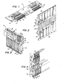
- a printed circuit board 10 which comprises a sheet of glass epoxy fiberglass laminate, often known as G-10 or FR-4.
- the printed circuit board material has been processed in the conventional manner so that a plurality of solder- coated copper conductors 11 are arranged on the board in a pre-selected pattern.
- the pattern is pre-selected to interconnect a plurality of circuit components which are mounted on the surfaces of the board (not shown) and also connect those components with circuitry external to the surface of the printed circuit board.
- the circuit points to be connected to circuitry external of the board include elongate solder- coated conductive strips 12 disposed parallel to and spaced from one another extending transversely along the linear edge 13 of the printed circuit board 10 on both the upper face and the lower face (not shown) of the board edge.
- the disclosure will use elongate rectangular conductive strips 12 as exemplary conductive circuit terminations along the board edge but it should be understood that these could consist of circular pads, dots or any other shape of conductive area to which the connector of the invention may be electrically joined, such as by solder.
- Disposed adjacent the edge 13 of the printed circuit board 10 is the printed circuit board edge connector of the present invention 14.
- the connector 14 includes a molded insulator 15 which is generally Y-shaped in cross-section.
- the forked end of the insulator includes a slotted head section 17 which receives and engages the flat straight edge 13 of the printed circuit board 10.
- the head section 17 is attached to a flat blade section 16 which includes a lower edge 18 having a bevel 19 for guiding the connector into the card slot of a conventional printed circuit board card edge connector.
- the blade section 16 comprises generally flat front and rear surfaces 21 which include parallel transversely extending recesses 22 formed therein and separated from one another by raised ribs 20.
- the slotted head section 17 includes a pair of parallel upstanding walls 42 and 43, the inner faces of which are spaced from one another a distance slightly greater than the thickness of the printed circuit board 10.
- the inner faces of the walls also include transverse recesses 44 and 45 in axial alignment with the blade recesses 22 and connected thereto by apertures 48 in the head section as will be more fully explained below.
- Elongate metal contacts 30 are received into each of the recesses 22 and extend through the apertures 48 in the head section 17, along the recesses 44 and 45 in the walls thereof, to be disposed in alignment with and overlying the solder coated conductive areas 12 along the front and rear surfaces of the board edge 13.
- the slot 41 of the slotted head section 17 of the connector 14 receives the edge 13 of the printed circuit board 10 in alignment in accordance with tooling holes on the board edge and aperatures 50 in the insulator and the contacts are soldered to the plated areas 12.
- FIG. 2 there is shown a section of an elongate metal strip 31 illustrating the manner in which the contacts 30 of the present connector are preferably formed by stamping with a progressive die.
- the strip 31 is formed of a material such as a cupro-nickel alloy and then processed in accordance with well known techniques to inlay a gold band 32 on the upper face of the strip.
- a pair of similar tin-lead bands (not shown) are inlaid on the opposite face of the strip from the gold bands near the outer edges thereof.
- the connector of the present invention lies a very distinct advantage of the connector of the present invention; namely, that the contacts 30 are formed in a fashion whereby gold inlaying processes may be used to add the gold band 32 to the interconnecting regions of the contacts effectively and with very little waste.
- Such bands are of a gold which is much less porous and of a more consistent and higher quality than that of plated gold which is most often used on prior art electrical contacts.
- the gold material forming the inlayed band 32 allows many more board insertion cycles per given plating thickness than plated interconnection fingers conventionally formed along one edge of a printed circuit board.
- each elongate contact 30 comprising a narrow first tail region 34, which is frangibly attached to a carrier strip 35 left intact along each edge of the strip 31, and a broader paddle shaped head region 36.
- the head 36 and tail 34 are separated by a shoulder region 80.
- the shoulder region 80 includes a pair of generally rectangular upwardly facing shoulders 81 and a pair of upwardly facing transversely resilient lance portions 82 bent out of the plane of the paddle region 36.
- the neck section of joinder 84 between the tail region 34 and the shoulders 81 is bent first out of the plane of the paddle region 36 and then back toward that plane so that the longitudinal axis of the tail 34 lies at an angular offset from the longitudinal axis of the paddle 36, as best seen in the final contact configuration shown in Fig. 4.
- the gold inlaid band 32 is positioned with respect to the contacts 30 so that the gold region form the electrical interconnecting portions of the contacts and the tin-lead regions on the opposite side (not shown) form the portions of the contacts along tail regions 34 to be joined to the edge of the printed circuit board.
- the interleafed contact arrangement of the flat pattern on the strip 31 insures maximum utilization of the gold inlaid material for electrical contacting regions.
- the contacts 30 are bent slightly about the neck section of joinder 84 so that the longitudinal axis of each contact head region 35 is displaced a small angular offset from the longitudinal axis of each contact tail region 34.
- the two rows of contacts 30 are separated from one another and each comprises an elongate carrier strip 35 having a plurality of contacts extending transversely thereof and being attached to the strip at their narrower end 34 by a frangible, reduced section.
- the insulator 15 is preferably formed by molding with conventional insulator materials such as a thermoplastic and includes a blade section 16 and a slotted head section 17 for receiving and engaging the edge of a printed circuit card.
- the insulator 15 is generally Y-shaped in cross-section.
- the forked card engaging head section 17 includes a printed circuit card receiving slot 41 formed by a pair of parallel upstanding walls 42 and 43 connected by a bottom surface 47 which physically abutts the edge of a printed circuit card when positioned in the insulator.
- the walls 42 and 43 are spaced from one another a distance slightly greater than the thickness of the mating printed circuit board to snuggly receive the edge of the board.
- the inner faces of the walls include a plurality of parallel, transversely extending recesses 44 and 45 separated from one another by ribs 46.
- Each recess 44 in wall 42 is transversely aligned with an opposing and facing recess 45 in wall 43.
- Each rib may include an optional circular aperture 50 extending coaxially through both walls of the head section for alignment and securement of the connector to the edge of the printed circuit board as will be discussed further below.
- the blade section 16 Extending from the head section 17, opposite the slot 41, is the blade section 16 which includes generally flat front and rear surfaces 21, each of which has formed therein a plurality of parallel transversely extending outwardly facing blade recesses 22. Each blade recess 22 is separated from an adjacent parallel recess by an upstanding rib 20.
- the heights of the ribs 20 are such as to provide an overall blade thickness approximately equal to the largest thickness of printed circuit card to be received into the card slot in a conventional card edge connector.
- the upstanding ribs 20 serve as self-centering means for the blade portion of the connector of the present invention.
- Each outwardly facing blade recess 22 is in general axial alignment with a conversely inwardly facing head wall recesses 44 or 45 and is connected thereto by a generally rectangular aperture 48 which passes through the bottom surface 47 of the head section 17 in alignment with the blade and head recesses.
- the aperture 48 include beveled upper edges to guide the insertion of contacts and a transversely extending, rectangular slot 49 which joins each aperture 48 to the slot 44 or 45 in the wall 42 or 43 at the juncture of the wall with the bottom 47. This allows the ready passage of contacts having an offset bend in the shoulder region as will be discussed below.
- the housing has a plurality of generally rectangular sleeves formed therein by the aligned combination of an inwardly facing rectangular head wall recess, a rectangular hole and a rectangular blade recess.
- the lower ends of the blade slots 22 are squared and of a depth greater than the thickness of the contact blade 35 to shield and protect the ends thereof from damage during insertion of the connector blade into an edge connector slot.
- the lower edge 18 of the blade 16 includes bevels 19 which serve to guide the blade portion of the connector into a conventional printed circuit card edge connector slot.
- FIG. 4 and 5 there is shown how the two opposed rows of contacts and the insulator 17 are brought together to form the connector assembly of the present invention.
- the two opposed rows of contacts are aligned with the angularly offset tail regions 34 and carrier strips 35 facing one another.
- Each of the contacts 30 are inserted into one for the insulator sleeves formed by an upper head recess 44, an aperture 48 and a blade recess 22.
- the blade portions 36 are inserted through the aperture 48 in the bottom 47 of the head section 17 and are moved down the blade recesses 22 until the contact blade tip reaches the lower end of each recess.
- the transversely resilient contact tails 34 extend toward one another and are separated by a distance less than the thickness of the printed circuit board edge to which the connector is to be affixed.
- the connector assembly may be transported or stored and used subsequently by attachment to the printed circuit board edge as shown in Figure 6.
- the insulator includes a plurality of transverse apertures 50, one between each of the sleeves 44 and 45 passing, through the ribs 46.
- This feature allows the insulator 15 to be molded in one standard length and then cut to a selected number of contact positions in length to fit particular applications which produces a substantial saving in stocking costs.
- a plurality of insulators can be placed end-to-end to make especially long edge connections.
- the solder coated conductive strip 12 on a printed circuit board 10 is brought into alignment with the connector by means of the apertures 50 in the insulator head apertures 50 in the insulator head apertures 49 in the edge of the printed circuit board so that the upper tail portions 34 of each contact 30 is generally coaxially aligned with a conductive strip 12.
- the spring like action of the angularly offset contact tails must be overcome to move the board 10 between the rows of contacts.
- FIG. 7 Also illustrated in Figure 7 is the manner in which optional square-wire posts 90 may be press-fitted through selected ones of the aperture 50 in the insulator and ones of the aligned apertures 49 in the edge of the positioned printed circuit board.
- the posts 90 may be used to provide strain relief for the mechanical solder connections between the connector contacts and the printed circuit board as required for certain MIL-spec connector applications.
- the aperture 50 and 49 may also be used to key proper alignment and positioning between the connector and conductive circuitry along the edge of the printed circuit board.
- the apparatus comprises a mounting plate 51 onto which is mounted an upper arm 52 and a lower arm 53 which are pivoted to one another by means of a hinge 54.
- the lower arm 53 is rigidly mounted to the plate 51 by means of beams 55 while the entire assembly is preferrably mounted in a box-like structural housing 56 shown in phantom.
- the upper arm 52 is biased downwardly toward the lower arm 53 by means of a pair of helical springs 58 and 59 which abut the upper surface of the housing 56 to provide a continual spring biased urge of the arms toward one another.
- the arms 52 and 53 are separated from one another by means of cam mechanism 61 which is affixed to an external actuation arm 62 and an interior strut 63 which is spring biased to a mount 64 on the rear wall of the housing 56 by means of a helical spring 65.
- the actuation arm 62 is shown in the raised position and the radially extending lobe 66 on the cam mechanism 61 is extended toward the upper arm 52 and separates the arms from one another against the spring bias.
- the front edge of the upper arm 52 includes an upper jaw member 71 while the lower arm 53 terminates in a lower jaw member 72.
- Each of the jaws respectively include an upper jaw edge 73 and a lower jaw edge 74.
- Mounted within each of the upper and lower jaw edges 73 and 74 are resistance heating mechanisms (not shown) which are conventional in nature and which are connected to a source of current by means of wires 75.
- An upper thermometer 77 and a lower thermometer 78 monitor the temperatures of the upper and lower jaw edges 73 and 74, respectively, to insure that the jaws have reached soldering temperature prior to actuation of the device.
- a positioning fixture 91 Mounted between the jaws and spaced slightly out of the path thereof is a positioning fixture 91 which includes a recess 92 therein for receiving the blade edge of the connector of the present invention and positions it by means of the depth of recess 82 to insure engagement of the jaws with the proper portion of the assembly.
- the upper and lower jaws 73 and 74 are shown in engagement with the assembly comprising the printed circuit board 10, the contacts 30 and the insulator 15.
- the jaws 73 and 74 lie flushly against the two mated surfaces which are in facing engagement to be joined; namely, the elongate solder coated conductive areas 12 on the upper and lower surfaces of the printed circuit board 10 and the tail portions 34 of the upper and lower rows of contacts 30.
- the heating mechanisms within the jaws 73 and 74 heats those surfaces to melt the solder carried by the conductive strips 12 and inlaid into the underside of the contact tails and join the strips to the contact tails 34.
- the opposed rows of contact tails 34 are bowed toward one another and, thus, the upper and lower surfaces of the printed circuit board 10. In this manner, when the solder is heated to melting temperature, the spring biased force holds the two parts in intimate engagement as the solder first flows and then is allowed to cool and solidify.
- the finished printed circuit board and finger connector combination is then completed by removing the upper and lower contact carrier strips 35 by flexing them about the point of joinder to the contact tails 34. This action breaks the reduced sections therebetween and separates the strips from the assembly.
- a completed connector and printed circuit board assembly may then be sued in the identical fashion as a printed circuit board having plated edge fingers.
- the connector contacts form an interconnection between the board and a printed circuit board edge connector; that is, the gold inlaid outer surfaces of the contact portions 36 will matingly engage the cantilever contact members of a conventional card edge connector.
- the sleeves and contacts may for special applications, be staggered on the insulator or made of different lengths to provide for sequential or selective interconnection with the contacts of the card edge connector.
- the printed circuit board finger connector of the present invention may not only be used to make connection with new printed circuit boards but may also be used highly effectively to repair printed circuit boards having old or damaged plated edge fingers.
- the contact tail portions 34, of the connector assemblies of Figures 6 and 7, are joined to the plated edge fingers of a board to be repaired just as they are joined to the plated conductive strips 12 of the printed circuit board 10.
- the spring biased contact tails 34 bear against the plated fingers and aid the soldering process by holding the parts to be joined in the engagement as solder is added. This feature permits the salvage of expensive fully fabricated and tested printed circuit boards which would otherwise be scrapped for defective construction or plating of the edge finger terminations.
- the printed circuit card finger connector of the present invention provides many advantages over the use of plated contact fingers along the edge of a printed circuit board and further includes many advantages over the prior art finger connectors. It is thus believed that the operation and construction of the present invention will be apparent from the foregoing description. While the method and apparatus shown and described has been characterized as being preferred, it will be obvious that various changes and modifications may be made therein without departing from the spirit and scope of the invention as defined in the following claims.
Landscapes
- Coupling Device And Connection With Printed Circuit (AREA)
- Multi-Conductor Connections (AREA)
Applications Claiming Priority (2)
| Application Number | Priority Date | Filing Date | Title |
|---|---|---|---|
| US41151682A | 1982-08-25 | 1982-08-25 | |
| US411516 | 1982-08-25 |
Publications (2)
| Publication Number | Publication Date |
|---|---|
| EP0101539A2 true EP0101539A2 (fr) | 1984-02-29 |
| EP0101539A3 EP0101539A3 (fr) | 1987-01-28 |
Family
ID=23629256
Family Applications (1)
| Application Number | Title | Priority Date | Filing Date |
|---|---|---|---|
| EP83105759A Withdrawn EP0101539A3 (fr) | 1982-08-25 | 1983-06-11 | Connecteur mâle rapporté pour carte à circuit imprimé et méthode de fabrication |
Country Status (2)
| Country | Link |
|---|---|
| EP (1) | EP0101539A3 (fr) |
| JP (1) | JPS5960869A (fr) |
Cited By (4)
| Publication number | Priority date | Publication date | Assignee | Title |
|---|---|---|---|---|
| EP0278779A3 (en) * | 1987-02-13 | 1989-05-03 | Switchcraft, Inc. | Slab-like jack module |
| EP0454977A1 (fr) * | 1990-03-16 | 1991-11-06 | Japan Aviation Electronics Industry, Limited | Connecteur à fiche électrique ayant des bandes de contacts encastrées dans une plaque isolante pour application aux plaquettes de circuits |
| EP0655809A3 (fr) * | 1993-11-30 | 1997-05-02 | Whitaker Corp | Connecteur de bord à profil bas. |
| WO2007143961A1 (fr) * | 2006-06-15 | 2007-12-21 | Siemens Aktiengesellschaft | Élément de connexion électrique |
Family Cites Families (9)
| Publication number | Priority date | Publication date | Assignee | Title |
|---|---|---|---|---|
| DE1911578A1 (de) * | 1969-03-07 | 1970-09-17 | Artos Engineering Co | Herstellungsverfahren fuer elektrische Anschluesse |
| FR2080252A6 (fr) * | 1970-02-27 | 1971-11-12 | Cit Alcatel | |
| US3894784A (en) * | 1972-07-14 | 1975-07-15 | Trw Inc | Plug connector for a printed circuit board |
| FR2239839A1 (en) * | 1973-07-31 | 1975-02-28 | Chauchat Jean | Male connector block for PCB has two forms - one with continuous contact strip with orthogonal pin, and other with two strips with spring arms |
| FR2254928A1 (en) * | 1973-12-12 | 1975-07-11 | Souriau & Cie | Connection device for printed circuit board - has insulating strip holding contacts on edge of board |
| GB1564928A (en) * | 1976-07-23 | 1980-04-16 | Ferranti Ltd | Edge connector plugs |
| FR2460552A1 (fr) * | 1979-07-02 | 1981-01-23 | Bunker Ramo | Carte imprimee avec embout ogival rapporte |
| US4216051A (en) * | 1979-07-11 | 1980-08-05 | Bell Telephone Laboratories, Incorporated | Apparatus for making bondable finger contacts |
| JPS5945197B2 (ja) * | 1980-07-15 | 1984-11-05 | 株式会社日立製作所 | プレス部品の加工法 |
-
1983
- 1983-06-11 EP EP83105759A patent/EP0101539A3/fr not_active Withdrawn
- 1983-08-25 JP JP58154262A patent/JPS5960869A/ja active Pending
Cited By (4)
| Publication number | Priority date | Publication date | Assignee | Title |
|---|---|---|---|---|
| EP0278779A3 (en) * | 1987-02-13 | 1989-05-03 | Switchcraft, Inc. | Slab-like jack module |
| EP0454977A1 (fr) * | 1990-03-16 | 1991-11-06 | Japan Aviation Electronics Industry, Limited | Connecteur à fiche électrique ayant des bandes de contacts encastrées dans une plaque isolante pour application aux plaquettes de circuits |
| EP0655809A3 (fr) * | 1993-11-30 | 1997-05-02 | Whitaker Corp | Connecteur de bord à profil bas. |
| WO2007143961A1 (fr) * | 2006-06-15 | 2007-12-21 | Siemens Aktiengesellschaft | Élément de connexion électrique |
Also Published As
| Publication number | Publication date |
|---|---|
| EP0101539A3 (fr) | 1987-01-28 |
| JPS5960869A (ja) | 1984-04-06 |
Similar Documents
| Publication | Publication Date | Title |
|---|---|---|
| US4572604A (en) | Printed circuit board finger connector | |
| KR900006067B1 (ko) | 칩 캐리어용 접촉자 및 그 삽입방법 | |
| EP0854549B1 (fr) | Connecteur pour le montage sur une surface avec assemblage intégré de circuit imprimé | |
| EP0651468B1 (fr) | Carte à circuits et connecteur en bordure, et procédé pour préparer le bord d'une carte à circuits | |
| US5277596A (en) | Method of producing a card edge mounted connector and the resulting assembly thereof | |
| EP0233914B1 (fr) | Connecteur de montage en surface | |
| US4381134A (en) | Electrical connector for plated-through holes | |
| EP0373342B1 (fr) | Assemblage de plaque de circuit et borne de contact utilisable dans ce circuit | |
| US4715820A (en) | Connection system for printed circuit boards | |
| US6379161B1 (en) | Method of making an electrical connector | |
| EP0147039A2 (fr) | Connecteur monté sur une surface | |
| EP0693796A1 (fr) | Connecteur avec des bandes métalliques comme membre de contacte, assemblage de connecteurs comprenant un tel connecteur | |
| US4920642A (en) | Method for connecting wires to an electrical connector | |
| US4421368A (en) | Lead-receiving socket, multi-socket assembly incorporating same and method of effecting circuit interconnections therewith | |
| KR960010739B1 (ko) | 인쇄 회로 기판의 제조 방법 및 인쇄 회로 기판 조립체 | |
| EP0479852B1 (fr) | Connecteur electrique pour connexion directe aux trous metallises pratiques dans une plaquette de circuits imprimes | |
| CA1178251A (fr) | Contact electriques en bandes | |
| EP0499431B1 (fr) | Mécanisme de retenue en forme de lance | |
| US3955877A (en) | Low profile contact | |
| EP0140473A1 (fr) | Conducteur sans soudure des plaquettes à circuit imprimé et dispositif de connexion utilisant celui-ci | |
| WO1998006149A1 (fr) | Connecteur electrique ayant des contacts minces a bords montes en saillie | |
| KR101683386B1 (ko) | 이중 두께 이중-단부형 수형 블레이드 단자 | |
| EP0101539A2 (fr) | Connecteur mâle rapporté pour carte à circuit imprimé et méthode de fabrication | |
| EP0468512A2 (fr) | Procédé et dispositif de connexion d'un connecteur à un câble | |
| US20050136710A1 (en) | Female Terminal for Inserting in a Printed Circuit Board |
Legal Events
| Date | Code | Title | Description |
|---|---|---|---|
| PUAI | Public reference made under article 153(3) epc to a published international application that has entered the european phase |
Free format text: ORIGINAL CODE: 0009012 |
|
| AK | Designated contracting states |
Designated state(s): BE CH DE FR GB IT LI |
|
| PUAL | Search report despatched |
Free format text: ORIGINAL CODE: 0009013 |
|
| AK | Designated contracting states |
Kind code of ref document: A3 Designated state(s): BE CH DE FR GB IT LI |
|
| STAA | Information on the status of an ep patent application or granted ep patent |
Free format text: STATUS: THE APPLICATION IS DEEMED TO BE WITHDRAWN |
|
| 18D | Application deemed to be withdrawn |
Effective date: 19870729 |
|
| RIN1 | Information on inventor provided before grant (corrected) |
Inventor name: EVANS, EVAN Inventor name: WEAVER, HARRY S. Inventor name: AMMON, PRESTON |