EP0101631A1 - Form zum Einkapseln von Elementteilen in Kunststoff - Google Patents
Form zum Einkapseln von Elementteilen in Kunststoff Download PDFInfo
- Publication number
- EP0101631A1 EP0101631A1 EP83201116A EP83201116A EP0101631A1 EP 0101631 A1 EP0101631 A1 EP 0101631A1 EP 83201116 A EP83201116 A EP 83201116A EP 83201116 A EP83201116 A EP 83201116A EP 0101631 A1 EP0101631 A1 EP 0101631A1
- Authority
- EP
- European Patent Office
- Prior art keywords
- mould
- blocks
- rods
- cavity
- cavities
- Prior art date
- Legal status (The legal status is an assumption and is not a legal conclusion. Google has not performed a legal analysis and makes no representation as to the accuracy of the status listed.)
- Granted
Links
Images


Classifications
-
- B—PERFORMING OPERATIONS; TRANSPORTING
- B29—WORKING OF PLASTICS; WORKING OF SUBSTANCES IN A PLASTIC STATE IN GENERAL
- B29C—SHAPING OR JOINING OF PLASTICS; SHAPING OF MATERIAL IN A PLASTIC STATE, NOT OTHERWISE PROVIDED FOR; AFTER-TREATMENT OF THE SHAPED PRODUCTS, e.g. REPAIRING
- B29C45/00—Injection moulding, i.e. forcing the required volume of moulding material through a nozzle into a closed mould; Apparatus therefor
- B29C45/17—Component parts, details or accessories; Auxiliary operations
- B29C45/26—Moulds
- B29C45/37—Mould cavity walls, i.e. the inner surface forming the mould cavity, e.g. linings
-
- B—PERFORMING OPERATIONS; TRANSPORTING
- B29—WORKING OF PLASTICS; WORKING OF SUBSTANCES IN A PLASTIC STATE IN GENERAL
- B29C—SHAPING OR JOINING OF PLASTICS; SHAPING OF MATERIAL IN A PLASTIC STATE, NOT OTHERWISE PROVIDED FOR; AFTER-TREATMENT OF THE SHAPED PRODUCTS, e.g. REPAIRING
- B29C33/00—Moulds or cores; Details thereof or accessories therefor
- B29C33/30—Mounting, exchanging or centering
- B29C33/301—Modular mould systems [MMS], i.e. moulds built up by stacking mould elements, e.g. plates, blocks, rods
-
- B—PERFORMING OPERATIONS; TRANSPORTING
- B29—WORKING OF PLASTICS; WORKING OF SUBSTANCES IN A PLASTIC STATE IN GENERAL
- B29C—SHAPING OR JOINING OF PLASTICS; SHAPING OF MATERIAL IN A PLASTIC STATE, NOT OTHERWISE PROVIDED FOR; AFTER-TREATMENT OF THE SHAPED PRODUCTS, e.g. REPAIRING
- B29C33/00—Moulds or cores; Details thereof or accessories therefor
- B29C33/56—Coatings, e.g. enameled or galvanised; Releasing, lubricating or separating agents
-
- H—ELECTRICITY
- H10—SEMICONDUCTOR DEVICES; ELECTRIC SOLID-STATE DEVICES NOT OTHERWISE PROVIDED FOR
- H10W—GENERIC PACKAGES, INTERCONNECTIONS, CONNECTORS OR OTHER CONSTRUCTIONAL DETAILS OF DEVICES COVERED BY CLASS H10
- H10W74/00—Encapsulations, e.g. protective coatings
- H10W74/01—Manufacture or treatment
- H10W74/016—Manufacture or treatment using moulds
-
- B—PERFORMING OPERATIONS; TRANSPORTING
- B29—WORKING OF PLASTICS; WORKING OF SUBSTANCES IN A PLASTIC STATE IN GENERAL
- B29C—SHAPING OR JOINING OF PLASTICS; SHAPING OF MATERIAL IN A PLASTIC STATE, NOT OTHERWISE PROVIDED FOR; AFTER-TREATMENT OF THE SHAPED PRODUCTS, e.g. REPAIRING
- B29C33/00—Moulds or cores; Details thereof or accessories therefor
- B29C33/0022—Multi-cavity moulds
-
- B—PERFORMING OPERATIONS; TRANSPORTING
- B29—WORKING OF PLASTICS; WORKING OF SUBSTANCES IN A PLASTIC STATE IN GENERAL
- B29C—SHAPING OR JOINING OF PLASTICS; SHAPING OF MATERIAL IN A PLASTIC STATE, NOT OTHERWISE PROVIDED FOR; AFTER-TREATMENT OF THE SHAPED PRODUCTS, e.g. REPAIRING
- B29C70/00—Shaping composites, i.e. plastics material comprising reinforcements, fillers or preformed parts, e.g. inserts
- B29C70/68—Shaping composites, i.e. plastics material comprising reinforcements, fillers or preformed parts, e.g. inserts by incorporating or moulding on preformed parts, e.g. inserts or layers, e.g. foam blocks
- B29C70/72—Encapsulating inserts having non-encapsulated projections, e.g. extremities or terminal portions of electrical components
-
- B—PERFORMING OPERATIONS; TRANSPORTING
- B29—WORKING OF PLASTICS; WORKING OF SUBSTANCES IN A PLASTIC STATE IN GENERAL
- B29K—INDEXING SCHEME ASSOCIATED WITH SUBCLASSES B29B, B29C OR B29D, RELATING TO MOULDING MATERIALS OR TO MATERIALS FOR MOULDS, REINFORCEMENTS, FILLERS OR PREFORMED PARTS, e.g. INSERTS
- B29K2909/00—Use of inorganic materials not provided for in groups B29K2803/00 - B29K2807/00, as mould material
- B29K2909/02—Ceramics
- B29K2909/04—Carbides; Nitrides
-
- B—PERFORMING OPERATIONS; TRANSPORTING
- B29—WORKING OF PLASTICS; WORKING OF SUBSTANCES IN A PLASTIC STATE IN GENERAL
- B29L—INDEXING SCHEME ASSOCIATED WITH SUBCLASS B29C, RELATING TO PARTICULAR ARTICLES
- B29L2031/00—Other particular articles
- B29L2031/34—Electrical apparatus, e.g. sparking plugs or parts thereof
- B29L2031/3406—Components, e.g. resistors
Definitions
- the invention relates to a mould for encapsulating parts of elements into a plastic material to manufacture electronic components, which mould comprises a number of steel blocks or rods, with accurately finished surfaces for clamping them completely tight together in a holder, in which clamped position recesses in said blocks or rods determine the mould cavity or mould cavities and the sprues, which mould has provisions for releasing the injected plastic material from the mould after hardening of said plastic and after opening of said mould.
- Such moulds are known from the prior art and these prior art moulds comprise a number of rods which accurately fitting can be clamped into a holder and which have a large number of mould cavities.
- Said rods have a length of approximately 200 mm, a height of approximately 15 mm and a width which is varying between 2 mm and for instance 60 mm, said width is dependent of the normalized dimensions of electronic components.
- the division up into rods or blocks is necessary because otherwise no accurate finishing of the mould cavities is possible, which mould cavities are lapped as smooth as possible.
- the blocks are very accurately finished to obtain a completely tight closure of the blocks against each other.
- the fluidized plastic material is not allowed to penetrate between the blocks.
- Said prior art moulds are very expensive and it is difficult to release the plastic after hardening.
- the plastic is a thermo hardening plastic which in the moulten condition is injected and hardens inside the mould.
- Said prior art moulds have very fine and very accurately finished passages for moving release pins there through. It will be clear that the plastic material is not allowed to penetrate into said passages.
- An object of the invention is now the provide a mould for encapsulating parts of elements into a thermohardening plastic, which mould is very easy to manufacture, and whereby releasing the encapsulating elements is very easy, so that automation is possible.
- the advantr-pes of this mould according to the invention are:
- moulds used with thermoplastic materials, with a hard nitride layer deposited by means of vapour deposition to extend the live of said mould.
- These moulds are however not suitable for encapsulating electronic parts.
- the dimensions of electronic components are very small and the requirements to the accuracy of the moulds are significantly higher than in the case of usual moulds for injection mould of thermoplastic or thermohardening material.
- the mould By making the mould of a sintered material, for instance sintered steel warpening during the depositioning of the nitride layer is avoided resulting into a mould with very favourable mechanical qualities.
- the mould such that the blocks or rods adjoining in longitudinal direction have such a small length that dimensional deviations of surfaces determining the mould cavity are within acceptable tolerance limits.
- the length of said blocks is in that case so small that eventual warpening because of the small length is hardly of any interest.
- the mould may have blocks or rods of which the dimensions in length, width and/or height direction are not or only slightly different, so that deformations of the shape caused by the high temperatures during the vapour depositioning of the nitride layer are in all directions approximatrely equal so that warpening is avoided.
- rods of the mould can be made flexible, so that warpened rods will be become straightened in the mould clamping device.
- a possibility therefore is providing the blocks or rods with transverse slots at that side turned away from the surfaces determining the mould cavity.
- warpening of the mould during the depositioning of the nitride layer can be restricted by the way in which the mould material is taken out of a piece of rolled steel. It appears the the warpening is minimized in case the direction in which the steel is rolled is perpendicular to the largest dimension of said blocks or rods, for instance perpendicular to the longitudinal direction.
- mould cavities It is known to configurate a mould with one or more series of mould cavities.
- the adjoining parts comprise in that case each a number of identical sections of the mould cavities and the sprues.
- the rows of connecting pins of integrated circuits are aligned to simplify the processing. If however the integrated circuits are mutually positioned such that the connecting pins are interlocking, then the mould cavities have to be dislocated turn and turn. That saves space so that a larger number of elements can be treated in one mould, however the mould itself becomes more expensive.
- each mould cavity or each pair of mould cavities is positioned into a separate block with the centerline at a distance from but parallel to the centerline of the mould.
- the layer provided by vapour depositioning in vacuum is a titanium nitride layer.
- Fig. 1 the block 1 of a mould is illustrated comprising the sprue 2.
- Said sprue is in agreement with the copending Dutch Patent Application 82,03253 positioned sidelong the mould, however, the sprue can also be positioned at the upper or lower side of the mould.
- the strip of material with the elements illustrated in Fig. 3 or 4 is placed onto the upper surface 14 of the block 1, whereby the connecting pins of the elements are fitting between the cams 9. It is important that the connecting pins are maintained free of plastic material so that afterwards it is possible to bend the connecting pins of the ready electronic component.
- the (not illustrated ) upper block is placed onto said block 1 such that the davel pins 8 of block 1 are fitting into said counterpart.
- thermo hardening fluid is injected through the sprue 2.
- the upper mould blocks are elevated and the treated element or strip of elements can be removed. Because of the presence of the hard titanium nitride layer in the mould cavity and in the sprue the plastic material will release without the use of releasing pins. Because furthermore the adherence of the plastic material is very poor pollution of the mould is prevented so that it is not necessary to clean the mould between the succeeding production steps. The result thereof is that a far reaching automation is possible.
- the illustrated mould block has an approximately square upper surface with a recess 4. The height is smaller than the width respectively the length. Provisions are taken to prevent warpening of the mould when the hard nitride layer is deposited by vapour deposition in vacuum because thereafter the mould cannot be lapped anymore.
- Fig. 2 a further embodiment of a mould block according to the invention is illustrated.
- This mould block has an elongated shape.
- This mould block has recesses 7 resulting into a flexible mould block.
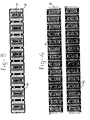
- a strip of material 10 in general copper with chips 11 and aligned connecting pins 6 is illustrated.
- the connecting pins 6 are turn and turn dislocated. That results into a shorter configuration so that in each mould a larger number of elements can be treatened.
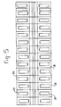
- FIG. 5 the positioning of the separate mould blocks 13 into a mould destined for treating a strip of material illustrated in Fig. 4 is shown.
- the separate mould blocks are comparable with the mould block of Fig. 2.
- the mould cavity 21 has a larger distance to the side 22 than the distance from the cavity 23 to the side 24, which difference in distance is determining for the dislocated configuration and thereforew is equal to half the distance 12 between the connecting pins 6 of Fig. 4.
Landscapes
- Engineering & Computer Science (AREA)
- Mechanical Engineering (AREA)
- Manufacturing & Machinery (AREA)
- Moulds For Moulding Plastics Or The Like (AREA)
- Encapsulation Of And Coatings For Semiconductor Or Solid State Devices (AREA)
- Casting Or Compression Moulding Of Plastics Or The Like (AREA)
- Physical Vapour Deposition (AREA)
- Injection Moulding Of Plastics Or The Like (AREA)
Priority Applications (1)
| Application Number | Priority Date | Filing Date | Title |
|---|---|---|---|
| AT83201116T ATE24069T1 (de) | 1982-08-19 | 1983-07-27 | Form zum einkapseln von elementteilen in kunststoff. |
Applications Claiming Priority (2)
| Application Number | Priority Date | Filing Date | Title |
|---|---|---|---|
| NL8203255A NL8203255A (nl) | 1982-08-19 | 1982-08-19 | Matrijs voor het met kunststof omhullen van delen van elementen. |
| NL8203255 | 1982-08-19 |
Publications (2)
| Publication Number | Publication Date |
|---|---|
| EP0101631A1 true EP0101631A1 (de) | 1984-02-29 |
| EP0101631B1 EP0101631B1 (de) | 1986-12-03 |
Family
ID=19840157
Family Applications (1)
| Application Number | Title | Priority Date | Filing Date |
|---|---|---|---|
| EP83201116A Expired EP0101631B1 (de) | 1982-08-19 | 1983-07-27 | Form zum Einkapseln von Elementteilen in Kunststoff |
Country Status (6)
| Country | Link |
|---|---|
| US (1) | US4546951A (de) |
| EP (1) | EP0101631B1 (de) |
| JP (1) | JPS5949917A (de) |
| AT (1) | ATE24069T1 (de) |
| DE (1) | DE3368151D1 (de) |
| NL (1) | NL8203255A (de) |
Cited By (1)
| Publication number | Priority date | Publication date | Assignee | Title |
|---|---|---|---|---|
| GB2170143A (en) * | 1985-01-28 | 1986-07-30 | Sumitomo Electric Industries | Die for use in forming lens |
Families Citing this family (9)
| Publication number | Priority date | Publication date | Assignee | Title |
|---|---|---|---|---|
| US4747864A (en) * | 1986-06-19 | 1988-05-31 | Corning Glass Works | Process for the precision molding of glass articles |
| EP0311711A1 (de) * | 1987-10-16 | 1989-04-19 | KLEVOTEC Gesellschaft für rechnergestützte Systemanwendungen mbH&Co.KG | Sintervorrichtung für Formlinge mit Hinterschneidungen aus schäumbarem Kunststoff |
| JPH01127122A (ja) * | 1987-11-10 | 1989-05-19 | Sumitomo Electric Ind Ltd | 焼結部品の成形あるいはコイニング、サイジング用金型 |
| US4861251A (en) * | 1988-02-29 | 1989-08-29 | Diehard Engineering, Inc. | Apparatus for encapsulating selected portions of a printed circuit board |
| GB2279025B (en) * | 1993-06-16 | 1997-01-15 | Nissan Europ Tech Centre | Casting model |
| JP2742514B2 (ja) * | 1993-11-30 | 1998-04-22 | 亞南産業株式會社 | 集積回路パッケージの成型方法 |
| WO2001020055A1 (en) * | 1999-09-10 | 2001-03-22 | Åmic AB | A method for the manufacturing of a matrix and a matrix manufactured according to the method |
| CN109016270A (zh) * | 2018-09-12 | 2018-12-18 | 珠海格力精密模具有限公司 | 模具装置 |
| CN115195033B (zh) * | 2021-04-12 | 2026-01-02 | 东莞市丞威塑胶制品有限公司 | 一种电子烟发热座注塑模具 |
Citations (4)
| Publication number | Priority date | Publication date | Assignee | Title |
|---|---|---|---|---|
| US2364745A (en) * | 1940-02-16 | 1944-12-12 | Gen Motors Corp | Mold equipment |
| FR1113670A (fr) * | 1953-11-16 | 1956-04-03 | Metallgesellschaft Ag | Outils de façonnage |
| DE1946961A1 (de) * | 1968-09-26 | 1970-04-02 | Ford Werke Ag | Stufenfoermiges Ziehwerkzeug mit Temperatursteuerung |
| DE2900114A1 (de) * | 1978-08-07 | 1980-02-14 | Dai Ichi Seiko Co Ltd | Spritzpressverfahren zum einkapseln von halbleitervorrichtungen |
Family Cites Families (7)
| Publication number | Priority date | Publication date | Assignee | Title |
|---|---|---|---|---|
| US2364746A (en) * | 1942-10-02 | 1944-12-12 | Kin O Lux Inc | Motion-picture mechanism |
| FR1113760A (fr) * | 1954-04-30 | 1956-04-04 | Villers Et Cie L | Perfectionnement aux machines à former les chapeaux |
| GB1261022A (en) * | 1968-01-22 | 1972-01-19 | Lucas Industries Ltd | Die and punch sets |
| GB1286330A (en) * | 1969-11-21 | 1972-08-23 | Electric Power Storage Ltd | Casting electric battery electrode grids |
| US4120930A (en) * | 1974-08-08 | 1978-10-17 | Lemelson Jerome H | Method of coating a composite mold |
| SE389456B (sv) * | 1975-01-29 | 1976-11-08 | Stenberg Flygt Ab | Gjutform |
| US4368168A (en) * | 1978-07-17 | 1983-01-11 | Dusan Slepcevic | Method for encapsulating electrical components |
-
1982
- 1982-08-19 NL NL8203255A patent/NL8203255A/nl not_active Application Discontinuation
-
1983
- 1983-07-27 EP EP83201116A patent/EP0101631B1/de not_active Expired
- 1983-07-27 DE DE8383201116T patent/DE3368151D1/de not_active Expired
- 1983-07-27 AT AT83201116T patent/ATE24069T1/de not_active IP Right Cessation
- 1983-08-12 JP JP58148677A patent/JPS5949917A/ja active Pending
- 1983-08-16 US US06/523,748 patent/US4546951A/en not_active Expired - Fee Related
Patent Citations (4)
| Publication number | Priority date | Publication date | Assignee | Title |
|---|---|---|---|---|
| US2364745A (en) * | 1940-02-16 | 1944-12-12 | Gen Motors Corp | Mold equipment |
| FR1113670A (fr) * | 1953-11-16 | 1956-04-03 | Metallgesellschaft Ag | Outils de façonnage |
| DE1946961A1 (de) * | 1968-09-26 | 1970-04-02 | Ford Werke Ag | Stufenfoermiges Ziehwerkzeug mit Temperatursteuerung |
| DE2900114A1 (de) * | 1978-08-07 | 1980-02-14 | Dai Ichi Seiko Co Ltd | Spritzpressverfahren zum einkapseln von halbleitervorrichtungen |
Cited By (2)
| Publication number | Priority date | Publication date | Assignee | Title |
|---|---|---|---|---|
| GB2170143A (en) * | 1985-01-28 | 1986-07-30 | Sumitomo Electric Industries | Die for use in forming lens |
| GB2170143B (en) * | 1985-01-28 | 1989-08-31 | Sumitomo Electric Industries | Die for use in forming lens |
Also Published As
| Publication number | Publication date |
|---|---|
| NL8203255A (nl) | 1984-03-16 |
| DE3368151D1 (en) | 1987-01-15 |
| JPS5949917A (ja) | 1984-03-22 |
| ATE24069T1 (de) | 1986-12-15 |
| US4546951A (en) | 1985-10-15 |
| EP0101631B1 (de) | 1986-12-03 |
Similar Documents
| Publication | Publication Date | Title |
|---|---|---|
| US4546951A (en) | Mould for encapsulating parts of elements into a plastic material | |
| WO2000078480A1 (en) | Multipiece core assembly for cast airfoil | |
| US3723585A (en) | Method of electroformed molds | |
| WO2000032331A1 (en) | Multipiece core assembly | |
| JPS62220244A (ja) | キヤビティにろうが充填されているセラミックコアの製造方法 | |
| EP0791446A3 (de) | Verbundkörper, Verfahren und Kunststoff-Spritzgiesswerkzeug zur Herstellung eines solchen | |
| CA1184671A (en) | Method of manufacture of plastics containers with incorporated heat sinks for integrated circuits and die and heat sink combination for use with this method | |
| CA2373428C (en) | A method of making a ceramic ornament having short undercuts on surface thereof | |
| GB2155395A (en) | Apparatus for flash-free insert molding | |
| US3840977A (en) | Method of making molds for molding or casting optical parts and the like | |
| US6010655A (en) | Method of making a ceramic ornament having short undercuts on surface thereof | |
| US4710332A (en) | Process of injection molding a laser mirror substrate | |
| KR100401068B1 (ko) | 캐리어 플레이트의 제조 방법 | |
| WO2002068147A1 (en) | Method for fabricating a plastic optic element injection mold | |
| CN120116310B (zh) | 一种杯把模具及其加工方法 | |
| EP0326214A1 (de) | Verfahren und Vorrichtung zum Herstellen einer magnetischen Halteplatte | |
| JP3050864B1 (ja) | 樹脂成形の金型 | |
| EP0411000A1 (de) | Herstellungsverfahren für schraubenrotoren. | |
| JPH02279311A (ja) | 成形型の製造法 | |
| JPH0243609B2 (ja) | Shashutsuseikeiyonotsukidashipinkoteihoho | |
| JPS594296B2 (ja) | 簡易型を用いた射出成形法 | |
| JPH0724652A (ja) | 成形金型の加工方法 | |
| SU1009686A1 (ru) | Способ изготовлени электрода-инструмента дл электрохимической обработки | |
| US2765268A (en) | Method of manufacturing casting moulds or pressing moulds | |
| KR20250026900A (ko) | 코어금형을 활용한 진공주형 장치 |
Legal Events
| Date | Code | Title | Description |
|---|---|---|---|
| PUAI | Public reference made under article 153(3) epc to a published international application that has entered the european phase |
Free format text: ORIGINAL CODE: 0009012 |
|
| AK | Designated contracting states |
Designated state(s): AT BE CH DE FR GB IT LI LU NL SE |
|
| RAP1 | Party data changed (applicant data changed or rights of an application transferred) |
Owner name: ARBO GEREEDSCHAPSMAKERIJ B.V. |
|
| 17P | Request for examination filed |
Effective date: 19840312 |
|
| GRAA | (expected) grant |
Free format text: ORIGINAL CODE: 0009210 |
|
| AK | Designated contracting states |
Kind code of ref document: B1 Designated state(s): AT BE CH DE FR GB IT LI LU NL SE |
|
| PG25 | Lapsed in a contracting state [announced via postgrant information from national office to epo] |
Ref country code: LI Effective date: 19861203 Ref country code: CH Effective date: 19861203 Ref country code: BE Effective date: 19861203 Ref country code: AT Effective date: 19861203 |
|
| REF | Corresponds to: |
Ref document number: 24069 Country of ref document: AT Date of ref document: 19861215 Kind code of ref document: T |
|
| ITF | It: translation for a ep patent filed | ||
| PG25 | Lapsed in a contracting state [announced via postgrant information from national office to epo] |
Ref country code: SE Effective date: 19861231 |
|
| ET | Fr: translation filed | ||
| REF | Corresponds to: |
Ref document number: 3368151 Country of ref document: DE Date of ref document: 19870115 |
|
| REG | Reference to a national code |
Ref country code: CH Ref legal event code: PL |
|
| PG25 | Lapsed in a contracting state [announced via postgrant information from national office to epo] |
Ref country code: LU Free format text: LAPSE BECAUSE OF NON-PAYMENT OF DUE FEES Effective date: 19870731 |
|
| PLBE | No opposition filed within time limit |
Free format text: ORIGINAL CODE: 0009261 |
|
| STAA | Information on the status of an ep patent application or granted ep patent |
Free format text: STATUS: NO OPPOSITION FILED WITHIN TIME LIMIT |
|
| 26N | No opposition filed | ||
| ITTA | It: last paid annual fee | ||
| PGFP | Annual fee paid to national office [announced via postgrant information from national office to epo] |
Ref country code: FR Payment date: 19920707 Year of fee payment: 10 |
|
| PGFP | Annual fee paid to national office [announced via postgrant information from national office to epo] |
Ref country code: GB Payment date: 19920717 Year of fee payment: 10 |
|
| PGFP | Annual fee paid to national office [announced via postgrant information from national office to epo] |
Ref country code: DE Payment date: 19920727 Year of fee payment: 10 |
|
| PGFP | Annual fee paid to national office [announced via postgrant information from national office to epo] |
Ref country code: NL Payment date: 19920731 Year of fee payment: 10 |
|
| PG25 | Lapsed in a contracting state [announced via postgrant information from national office to epo] |
Ref country code: GB Effective date: 19930727 |
|
| PG25 | Lapsed in a contracting state [announced via postgrant information from national office to epo] |
Ref country code: NL Effective date: 19940201 |
|
| NLV4 | Nl: lapsed or anulled due to non-payment of the annual fee | ||
| GBPC | Gb: european patent ceased through non-payment of renewal fee |
Effective date: 19930727 |
|
| PG25 | Lapsed in a contracting state [announced via postgrant information from national office to epo] |
Ref country code: FR Effective date: 19940331 |
|
| PG25 | Lapsed in a contracting state [announced via postgrant information from national office to epo] |
Ref country code: DE Effective date: 19940401 |
|
| REG | Reference to a national code |
Ref country code: FR Ref legal event code: ST |