EP0101941A2 - Atténuateur rapide de grande puissance à échelons, méthode et appareil - Google Patents
Atténuateur rapide de grande puissance à échelons, méthode et appareil Download PDFInfo
- Publication number
- EP0101941A2 EP0101941A2 EP83107415A EP83107415A EP0101941A2 EP 0101941 A2 EP0101941 A2 EP 0101941A2 EP 83107415 A EP83107415 A EP 83107415A EP 83107415 A EP83107415 A EP 83107415A EP 0101941 A2 EP0101941 A2 EP 0101941A2
- Authority
- EP
- European Patent Office
- Prior art keywords
- signal
- port
- input
- output port
- transmission line
- Prior art date
- Legal status (The legal status is an assumption and is not a legal conclusion. Google has not performed a legal analysis and makes no representation as to the accuracy of the status listed.)
- Granted
Links
- 238000000034 method Methods 0.000 title claims abstract description 8
- 230000006798 recombination Effects 0.000 claims abstract description 6
- 238000005215 recombination Methods 0.000 claims abstract description 6
- 230000005540 biological transmission Effects 0.000 claims description 34
- 230000010363 phase shift Effects 0.000 claims description 21
- 230000008878 coupling Effects 0.000 claims description 9
- 238000010168 coupling process Methods 0.000 claims description 9
- 238000005859 coupling reaction Methods 0.000 claims description 9
- 230000002238 attenuated effect Effects 0.000 claims description 8
- 230000002441 reversible effect Effects 0.000 claims description 4
- 239000000654 additive Substances 0.000 claims description 3
- 230000000996 additive effect Effects 0.000 claims description 3
- 238000002955 isolation Methods 0.000 abstract description 7
- 239000003990 capacitor Substances 0.000 description 8
- 230000035882 stress Effects 0.000 description 4
- 230000000903 blocking effect Effects 0.000 description 3
- 238000010586 diagram Methods 0.000 description 3
- 230000008901 benefit Effects 0.000 description 2
- 230000003247 decreasing effect Effects 0.000 description 2
- 230000000694 effects Effects 0.000 description 2
- 230000014509 gene expression Effects 0.000 description 2
- 230000001902 propagating effect Effects 0.000 description 2
- 230000004044 response Effects 0.000 description 2
- 241000283986 Lepus Species 0.000 description 1
- 230000003679 aging effect Effects 0.000 description 1
- 230000008859 change Effects 0.000 description 1
- 238000012790 confirmation Methods 0.000 description 1
- 239000003989 dielectric material Substances 0.000 description 1
- 238000012986 modification Methods 0.000 description 1
- 230000004048 modification Effects 0.000 description 1
- 230000000063 preceeding effect Effects 0.000 description 1
- 230000000644 propagated effect Effects 0.000 description 1
- 230000000007 visual effect Effects 0.000 description 1
Images

Classifications
-
- H—ELECTRICITY
- H03—ELECTRONIC CIRCUITRY
- H03H—IMPEDANCE NETWORKS, e.g. RESONANT CIRCUITS; RESONATORS
- H03H7/00—Multiple-port networks comprising only passive electrical elements as network components
- H03H7/24—Frequency- independent attenuators
-
- H—ELECTRICITY
- H01—ELECTRIC ELEMENTS
- H01P—WAVEGUIDES; RESONATORS, LINES, OR OTHER DEVICES OF THE WAVEGUIDE TYPE
- H01P1/00—Auxiliary devices
- H01P1/22—Attenuating devices
- H01P1/227—Strip line attenuators
Definitions
- the present invention is directed to attenuation of electromagnetic signals, and particularly to a high speed step attenuator and attenuation method for high frequency, high power signals.
- One of the attenuators discussed in the article involves the use of a pin diode which is employed as a variable resistance element.
- the pin diode is connected in shunt across a transmission line.
- a DC biasing voltage is applied to the pin diode in order to select a specific attenuating resistence value.
- a capacitance is required in series with the diode in order to resonate the intrinsic inductance and reverse capacitance of the diode out of the circuit.
- Attenuator Another embodiment of attenuator is discussed in the above identified article, one which employs selectable parallel signal paths, one path having no attenuation therein and the other signal path having a matched, resistive attenuation.
- the switching between signal paths is obtained by appropriately biasing pin diodes into a conducting or non-conducting state.
- several of these parallel signal path circuits could be connected in series, with each of the circuits providing a different degree of resistive attenuation, so that by selecting combinations of the various attenuation factors, the desired total attenuation can be obtained.
- One of the drawbacks of such a configuration is the high component count required. For example, at least two pin diodes are required for each signal path, with it being recommended that several pin diodes be used in place of a single pin diode, in order to provide adequate isolation. Additionally, it is recommended that pi or tee networks be used for the resistive attenuation elements. This is based upon the need to avoid any impedance mismatches in the circuit to prevent reflected waves from being returned to the input of the attenuator. These tee or pi networks require a minimum of three resistive components to implement.
- a further drawback of this second configuration is that the pin diodes are used as switches therein and are therefore subjected to high power levels. This can lead to component failure, or a shortened component life.
- the connection of the pin diodes in series with the signal paths renders heat sinking of the diodes difficult, thereby further complicating thermal requirements, such as the maintaining the temperature of the diode junction below a maximum temperature.
- a drawback which is common to both of the above discussed attenuator configurations is the speed by which the pin diodes can be switched off and on or from one bias point to another.
- the switching time of the pin diodes is often less than satisfactory. This is due, especially in the second configuration, to the high operating signal levels of the various pin diodes. In such a high power operating mode, the intrinsic capacitance of the diode is substantial and as such, there is a bothersome response time between the application of the command to switch between states and the actual switching of the pin diodes ..between states.
- T hus there is a long-felt need for a high frequency, high speed, high power.step attenuator in which the component count is reduced, the operating stress upon the components decrease, and the switching time between steps decreased.
- a high speed, high power step attenuator comprising means for providing signal paths between an input port, a first output port, a second output port and a termination port which-splits an input signal presented at the input port into a first split signal and a second split signal, both of substantially equal magnitude.
- the first split signal is supplied to a first signal path, between the input port and the first output port, and the second split signal is applied to a second signal path, between the input port and the second output port.
- the first and second signal paths are constructed to impart a phase shift to any signals traveling thereon so as to isolate the input port from any portions of the input signal which are reflected back to the input port due to mismatches at the output ports.
- the paths between the ports are also arranged so that these reflected waveforms are routed to the termination port for dissipation there.
- Means are provided for selectively introducing an impedance mismatch at the first and second output ports so that substantially equal portions of the first and second split signals are reflected back into the input signal splitting means and so that substantially equal portions of the first and second split signals are transmitted to a recombining means.
- These transmitted portions of--the first and second split signals are operated upon in the recombining means to be in phase with each other at an output port of the recombining means, so that an additive recombination of the transmitted signals is achieved at the recombining means output port.
- the-mismatch means comprise resistive elements which are electrically connected to the first and second output ports of the input signal splitting means and which are switched in and out of parallel connection with the first and second output ports by pin diodes.
- these pin diodes are operating at a lower signal magnitude than in prior art attenuators, due to the splitting of the input signal between first and second signal paths. As a result of this lower operating magnitude, the pin diodes can be made to switch faster between an off and on state.
- the input signal splitting means provides isolation between the first and second output ports and the input port the problem of reflected waveforms due to mismatches in the signal path is solved. Instead of having to contend with reflected waveforms at the input port of the attenuator, as in the prior art, the problem is overcome by routing the reflected waveforms to the termination port for dissipation there.
- the pin diodes are used as high speed microwave switches rather than variable resistive elements, there is little effect on the performance of the attenuator due to temperature variation or aging effects upon the pin diode. Moreover, the component count can be significantly reduced because isolation problems, due to the capacitance of the pin diode, are less pronounced in configuration of the present invention as compared to that of the prior art.
- the present invention can handle high signal power levels, first of all, due to the splitting of the signal magnitude equally between two parallel signal paths, and second of all, because in every case, the pin diodes are connected in series with some resistive element so as to further reduce the power handling requirements for each pin diode.
- the pin diodes are switching resistive elements in parallel with the signal paths of the attenuator, the value of the mismatch, or attenuation, obtained can be controlled precisely by controlling the precision of the resistive elements used.
- no special temperature compensated DC biasing circuit is required to set the bias on each pin diode to a precise level. As such, the-complexity of the step attenuator is significantly reduced.
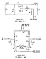
- FIG 1 a prior art step attenuator is shown.
- a pin diode 10 is provided with selected magnitudes of bias voltages via line 12, radio frequency choke 14, and bypass capacitor 16.
- the characteristic impedance of the RF signal path 18 is R.
- the pin diode 10 is biased for a resistance having a magnitude different from R , a mismatch is set up in the signal path 18. This causes a portion of the signal, which impinges upon the diode, to be reflected back to the input port with the remainder of the signal being transmitted to the output port. From Figure 1 it can be seen that no provision is provided for dissipation of this reflected input signal component.
- a further drawback of this configuration is the need to resonate the intrinsic inductance 20 of the pin diode 10 in its off state.
- Capacitor 22 is shown connected in series with pin diode 10 in order to effectuate this requirement. As a result of this resonant condition, the bandwidth of the configuration is greatly limited.
- Figure 2 illustrates another prior art step attenuator configuration.
- the RF signal is switched between one of two signal paths 24 and 26 by way of series connected pin diodes 28.
- the pin diodes are switched on and off by way of biasing voltages.
- the biasing voltage -to signal path 24 is supplied through radio frequency chokes 30, 32, and 34, while biasing voltages for path 26 are supplied through radio frequency chokes 36 and 32 as well as 38 and 34.
- signal path 24 does not provide any attenuation to the input signal, while path 26 provides resistive attenuation in series with the signal path.
- this resistive attenuation takes the form of a pi or tee network in order to maintain the characteristic impedance of the signal path, and thus avoid any reflected waveforms.
- the pin diodes in signal path 24 are required to handle the full power of the input signal. As such, the maximum power capable of being handled by such an attenuator is limited by the power dissipation capabilities of these pin diodes. Additionally, because the pin diodes are handling signals of such high power level, switching these diodes from an on to an off state is a significant problem which limits the speed by which the attenuator can be switched from one level of attenuation to the next.
- FIG. 3 is a simplified function block diagram on the present invention.
- the present invention is connected in a microwave transmitting system which includes a transmitter 66 as the input signal source, and a duplexer 61 and a number of antennas 63 as the load for the attenuated signal.
- the transmitter supplies control signals to control circuitry 84 which in turn selects the attenuation desired.
- the input signal is applied from the transmitter 66 via an input port 40 to a signal splitter 42.
- the signal splitter 42 divides the input signal into first and second signal of substantially equal magnitude but different phase.
- the first and second signals are output from the splitter via a first output port 44 and a second output port 46, respectively.
- Connected to the first and second output ports 44 and 46, are mismatch circuits 48 and 50. These are controlled by signals on lines 52 from control circuit 84 by which the mismatches can be removed or connected to the first and second output ports 44 and 46.
- the waveforms which are reflected back into the signal splitter 42 are routed by signal splitter 42 to a termination port 59 where the signals are dissipated in a match load. No portion of the reflected signals appears at input port 40 because the phase relationships of the signal paths within the signal splitter 42 cause the reflected waveforms to cancel one another at the input port 40.
- the present invention implements a method of high power, high frequency, high speed step attenuation by splitting the input signal into two signals having substantially the same magnitude but different phases; by subjecting the signals to a selected mismatch so that a portion of the signals are reflected back towards the input part of the attenuator and the remaining portion transmitted to a summing circuit; by adjusting the phase of the transmitted portions of the signal so that they are in phase with one-another at the output of the summing circuit; by isolating the input port of the attenuator from the reflected waveforms due to the mismatches; and by dissipating the reflected waveforms in_a matched, termination load.
- the mismatches are switched in and out of the signal paths by way of pin diodes.
- Figure 4 illustrates an embodiment of the present invention which provides attenuation of high power signals in one decibel (dB) selectable steps from zero dB to 41 dB.
- dB decibel
- three stages, 58, 60 and 62, of the basic attenuator circuit are connected in series.
- a detailed description will be given of the basic attenuator circuit, it being an obvious step to select the mismatch values to form a particular stage in the overall attenuator, as well as to connect the various attenuator stages in series.
- Attenuator stage 58 the basic attenuator circuit will be described in greater detail.
- the characteristic impedance of the system in which the step attenuator circuit is to be used is 50 ohms.
- the signal paths of the step attenuator are designed for a 50 ohm system. It is to be understood where the characteristic impedance of the system in which the step attenuator is located differs, that the characteristic impedance of the step attenuator can be adjusted accordingly.
- the Signal Splitter 42 The Signal Splitter 42
- the signal splitter 42-of Figure 3 takes the form of a 3dB quadrature coupler 64.
- a 3dB quadrature coupler such as coupler 64, provides to port 44, via signal path 68, a signal which has been shifted in phase by 90 degrees from the input signal, and reduced in magnitude by 3dB.
- the signal path shown by arrow 70 provides to output port 46 a signal which has not been shifted in phase with respect to the input signal, but which has a magnitude which is 3dB below the input signal magnitude.
- Signal path 68 imparts a 90 degree phase shift by causing the input signal to electrically propagate along a quarter wavelength distance.
- the signal path 70 between input port 40 and output port 46 takes the form of electromagnetic coupling between signal path 68 and signal path 72, hence there is no phase shift due to such a path.
- Signal path 72 connects output port 46 to termination port 59. Signals traveling along this path are shifted in phase by 90 degrees due to the quarter wavelength of the path.
- the signal path is provided between output port 44 and termination port 59 via the electromagnetic signal path indicated by arrows 74. In both signal paths 70 and 74, the degree of the electromagnetic coupling along each path causes each resulting signal magnitude to be 3dB below that of the input signal..
- the input signal is introduced at input port 40 and caused to propagate to output port 44 via signal path 68, and to output port 46 via signal path 70.
- the signal appearing at output port 44 is shifted in phase by 90 degrees and, due to the coupling between signal path 68 and signal path 72, has a magnitude 3dB below the input signal magnitude.
- the signal presented to output port 46 is 3dB below the input signal magnitude but is of the same phase as the input signal.
- the reflected signal into output port 46 will be coupled via signal paths 70 back to input port 40.
- This reflected waveform will incur no phase shift upon etracing signal path 70, and will therefore be in )hase with the input signal. Because the magnitudes of the two reflected waveforms are the same and because :he two waveforms are 180 degrees out of phase at the Lnput port 40, they will cancel one-another.
- the input bort 40 is thus isolated from any reflected waveforms which enter output port 44 and 46 as a result of nismatches at these ports.
- While the reflected waveforms are self-cancelling 3 t input port 40, signal paths 72 and 74 route these reflected waveforms'to termination port 59 for dissipation in a matched load 76.
- the reflected waveform into output port 44 is coupled via signal path 74 to termination port 59.
- the signal at termination port 59 due to the reflected signal at output port 44 is 90 degrees out of phase from the original input signal.
- the reflected signal from output port 46 is coupled to termination port 59 via signal path 72.
- a signal transvers- ing signal path 72 will incur an additional 90 degree phase shift.
- the signal at termination port 59-due to the reflected waveform from output port 46 will be 90 degrees out of phase from the input signal.
- the reflected signals presented to dissipation port 59 will be in phase with each other.
- Termination load 76 for this embodiment is a 50 ohm load, and is designed to dissipate these reflected waveforms.
- quadrature coupler 64 input port 40 is isolated from reflected waveforms into output ports 44 and 46, while termination port 59, in conjunction with termination load 76 dissipates all of the reflected waveforms.
- mismatch means 48 and 50 are provided at output ports 44 and 46 of coupler 64 by way of resistive elements connected in series with pin diode switches. The series combination of pin diode switch and resistive element are applied in parallel to the signal paths.
- two pairs of mismatch elements 77 and 86 are shown connected to output ports 44 and 46 of coupler 64.
- Resistor 78 provides the impedance mismatch to the signal path, while capacitor 80 is a DC blocking capacitor as well as a resonating capacitor.
- Diode 82 when forward biased, connects resistor 78 in parallel with output port 44. When diode 82 is reversed biased, resistor 78 is taken out of the signal path.
- driver circuit 83 The forward or reverse biasing of diode 82 is performed by driver circuit 83.
- each mismatch element would have a pin diode switch which is controlled by a driver circuit.
- These drivers would be contained within a control circuit 84, which in turn receives control signals from the operating system, such as a transmitter 66. See Figure 3.
- Each driver circuit would be controlled by the operating system and the output of each driver would be selected by the operating system so that particular combinations of mismatches would be inserted into the corresponding signal paths to produce the desired amount of attenuation.
- the pin diode driver provides an initial high current spike to overcome the internal capacitance of the diode, followed by a steady state DC voltage to hold the diode in either a forward biased or reversed biased state. Because in the present invention the operating power levels are significantly lower for the various diode switches, as compared to prior step attenuator designs, the switching speed of the diodes can be significantly improved. In practice switching speeds of better than one microsecond have been achieved where the power of the input signal is on the order of two kilowatts.
- capacitor 80 is selected to resonate with the intrinsic inductance of the pin diode 82 in its on state. Due to the series connection of the diode in the mismatch element circuit, the effects of the internal inductance of the diode are not as pronounced as in the circuits of the prior art. Thus, the bandwidth of a step attenuator built according to the teaching of the present invention is at least an octave wide.
- mismatch element disposed at output port 46 which is substantially identical in component value to that disposed at output port 44. This is to provide substantially the same degree of mismatch at each of the output ports 44 and 46 so as to permit the cancellation of the reflected waveforms at input port 40 as discussed above.
- a second pair 86 of mismatch elements are positioned at output ports 44 and 46.
- This mismatch pair 86 provides a different degree of impedance i mismatch.
- the first pair of mismatched elements utilize a 200 ohm resistive element for a mismatch which provides approximately 1dB of attenuation, while the second mismatch pair 86 utilizes a 90 ohm resistive element to provide a mismatch which corresponds to approximately 2d B of attenuation.
- these mismatched elements can be connected into the signal paths either singlely or in combination, to thereby obtain attenuations of ldB, 2dB or 2.8dB.
- the attenuation of a resistor element, R, in parallel with a transmission line with characteristic impedance Ro is given by the equation 10 log 10 dB.
- the values of the resistive elements can be chosen for an infinite number of different attenuation values.
- the resistive elements of the first stage 58 are chosen to provide 1dB, 2dB and 2.8dB of attenuation.
- the resistive elements:of the second stage 60 are chosen to provide 4dB, 8dB or 9.8dB of attenuation.
- the resistive elements of the third stage 62 are chosen to provide 14 or 28dB of attenuation.
- the Summing Means 54 are The Summing Means 54
- the summing circuit 54 of Figure 3 is implemented by way of a second 3dB quadrature coupler 88.
- This coupler 88 is used in what can be termed a mirror image of coupler 64.
- the signal transmitted through the mismatch on signal path 90 is received by input port 94 of coupler 88.
- the signal on signal path 90 corresponds to the transmitted portion of the signal from output port 44 of coupler 64 which has been subjected to an impedance mismatch by either mismatch element 77 and/or 86.
- the signal is phase shifted by 90 degrees from the original input signal at input port 40 of coupler 64.
- Input port 96 receives the transmitted signal on signal path 92.
- the signal on signal path 92 is in phase with the input signal originally applied to port 40 of coupler 64, and is the transmitted portion of the signal from output port 46 of coupler 64 which has been subjected to the corresponding mismatch combination of mismatch element 77 and/or 86.
- quadrature coupler 88 provides signal paths which shift the phase of the signals traveling thereon depending upon the ports between which the signals are traveling.
- the output port of coupler 88 is selected so that the signal entering the input port 94 will follow signal path 98 and hence, will receive no phase shift.
- the signal inserted at input port 96 will propagate down signal path 100 and, as a result, be phase shifted by 90 degrees.
- the two signals will be in-phase at output port 97 of coupler 88.
- coupler 88 provides a phase shifting of the input signals and a summation of the phase shifted signals so that the resulting output signal at .
- output port 97 is reduced in magnitude from the magnitude of the input signal applied to input port 40 by an amount of attenuation determined by mismatch elements 77 and/or 86.
- Termination port 102 of coupler 88 is terminated ,in a 50 ohm load. From Figure 4 it can be seen that there is no signal dissipation in this termination due to the phase relationship of the signals at that port. That is, the signal applied to input port 94 will be shifted by 90 degrees at port 102, while the signal applied to input port 96 will not be shifted in phase. The result is one signal which is phase shifted by 180 degrees from the original input signal at input port 40, and another signal which is in phase with the original input signal at input 40 such that the two signals cancel each other at termination port 102 of coupler 88.
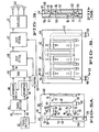
- FIG. 5 a physical implementation of one embodiment to the present invention will now be described.
- This implementation utilizes stripline transmission line techniques for use in the 16 Hz frequency range.
- the three stages of attenuation can be packaged tightly for a small space requirement.
- the horizontal dimension is approximately 3 1/4 inches
- the vertical dimension is approximately 2 1/2 inches
- the depth is approximately 1/2 inch.
- FIG. 5 In the implementation shown in Figure 5 two sides of a dielectric sheet 104 are utilized, with circuit traces on either side.
- the top view is shown with traces and components found on the top side drawn in solid lines, and with the traces and components found on the bottom of the sheet 104 bottom shown in dashed lines.
- Figure 5B is a side view of the embodiment of Figure 5 which shows the placement of the ground planes 106 and 108 which form a part of the stripline transmission line.
- Figure 5B illustrates the manner in which the signal traces of stripline are position on either side of the dielectric sheet 104, and sandwiched between ground planes 106 and 108.
- Figure 5A is a expanded view-of section 58 of Figure 5.
- the relative sizes of the various components and circuit traces are exaggerated.
- traces and components which are found on the top side of the dielectric sheet 104 are drawn with solid lines while the traces and components found on the bottom side of the dielectric sheet 104 are drawn in dotted lines.
- the reference numerals utilized in discussing the schematic diagram of Figure 4 are also utilized in discussing the physical circuit of Figure 5A. This is to facilitate the association of the physical components of the embodiment in 5A with the schematic representation of the components in Figure 4.
- the signal splitter 42 of Figure 3, or the quadrature coupler 64 of Figure 4 is formed by the trace segment on the top side of the board with reference numeral 68, and the trace segment on the bottom side of the board with reference numeral 72.
- the input port to quadrature coupler 64 is on the top side of the board and indicated by reference numberal 40.
- the first output port- f- from which is obtained the signal which is phase shifted by 90 degrees from the signal at the input port 40, is found at the other end of trace segment 68 and indicated by reference numeral 44.
- the second output port which provides the signal which is in phase with the signal presented at input port 40, can be found aligned with input port 40 and labeled with reference numeral 46.
- the termination port 59 At the other end of trace segment 72 is found the termination port 59. Note that the termination port 59 is disposed beneath the first output port 44. Note also that trace segment 68 is disposed directly above trace segment 72.
- the input signal is supplied to input port 40 of quadrature coupler 64 by trace segment 108, which is a length of stripline transmission line having a characteristic impedance of 50 ohms, via a Type SMA connector 106.
- trace segment 108 is a length of stripline transmission line having a characteristic impedance of 50 ohms, via a Type SMA connector 106.
- connector 106 can be any connector suitable for connecting high frequency signals from a cable or other signal line device to a circuit board trace.
- the length of trace segment 68 and of trace segment 72 is selected to be approximately a quarter wave length of the frequency of the signal being attenuated. In the case of the embodiment shown in Figure 5, a signal of approximately lGHz is desired to be attenuated thus indicating a quarter wave length of approximately 1 1/2 inches.
- both trace segment 72 and trace segment 68, as well as the dielectric material and spacing between trace segments 72 ahd 68, are chosen so that the signal which propagates electrically along each trace segment and the signal which is coupled electromagnetically between aligned ports have the same magnitude.
- the signal which emerges from port 44 will have a magnitude which is 3dB lower than the input signal and a phase which is shifted by 90 degrees from the input signal.
- the signal which emerges at output port 46 will have a magnitude which is 3dB lower than the magnitude of the input signal and a phase which is the same as the input signal.
- an advantage of splitting the signal into two separate signals having the same magnitude before actual attenuation is performed is that the amount of stress to which the attenuating components are subjected is significantly reduced. Additionally, this splitting of the input signal and the phase shifting of one split signal with respect to the other, by way of a quadrature coupler, permits a mismatch type of attenuation to be performed. This is because any reflected signals, due to the mismatches imposed, will be reflected back into the quadrature coupler 64 but phase-shifted by the coupler in such a way that the input port 40 is isolated from such reflected waveform, while the termination port 59 receives all of the reflected wave form magnitude for dissipation of the reflected waveforms there.
- This isolation and dissipation of the reflected wave forms is based upon the assumption that the reflected waveforms which propagate back through the quadrature coupler 64 to the input port 40 are impressed with a phase and magnitude such that they cancel one another out at the input port 50. Conversly it is assumed that, as the reflected signals propagate back through the quadrature coupler 64 toward the termination port, they are impressed with a phase shift and magnitude such that the sum of the reflected signals at termination port 59 is maximized, for complete attenuation of all of the reflected signals at termination.port 59.
- any coupler which provides the requisite isolation of the input port from the two output ports with respect to waveforms reflected back into the output ports, and which provides the requisite dissipation of the reflected waveforms, would be satisfactory for use in the present invention.
- the teaching of the present invention is not limited to splitting the input signal into two equal parts. Rather, it is the concept of reducing the signal magnitudes presented to the attenuating components by splitting the input signal into several parts, however many that may be, which is one of the teachings of this invention.
- Mismatch circuit 86 is disposed on trace segment 90 opposite mismatch circuit 77. As described in connection with Figure 4, the value of the resistive element of mismatch circuit 86 is selected to provide ' a different degree of impedance mismatch than that presented by resistive element 78 of mismatch circuit 77. With respect to trace segment 92, it can be seen that there is a corresponding mismatch circuit 77 and a corresponding mismatch circuit 86 positioned thereon.
- the pin diode corresponding to the particular resistive element is forward biased by driver circuit 84. This connects the desired resistive elements in parallel with the trace segments to form a mismatch of impedance in the signal paths.
- a portion of the signals propagating on trace segments 90 and 92 is reflected back to quadature coupler 64 while the remaining portion is permitted to continue on to quadrature coupler 88.
- quadrature coupler 88 corresponds to the summing circuit 54 of Figure 3.
- the amount of mismatch imposed upon signal paths 90 and 92 determines the amount of attenuation eventually achieved by the attenuation stage.
- mismatch circuits 77 and 86 provides a selectable number of steps of attenuation.
- the resistive element for mismatch 77 is selected to be 96 ohms while the resistive element for mismatch element 86 is selected to be 208 ohms.
- Connection of mismatch circuit 86 in parallel with trace segments 90 and 92 produces a 1dB attenuation while connection of the mismatch circuit 77 produces a 2dB attenuation.
- Connection of both mismatch circuits 77 and 86 produces a 2.8dB attenuation.
- by selecting the values of the resistive element one can obtain any degree of attenuation in any step size magnitude desired.
- resistive elements such as chip resistors are utilized in the embodiment discussed above, other ⁇ resistive elements, such as appropriately biased pin diodes can be used satisfactorily with the present invention.
- the quadrature coupler 64 splits the input signal into two signals having equal magnitude
- the mismatch circuits would be chosen so that the magnitude of reflection obtained thereby for each trace segment would be set so that there would be a cancellation of the reflected waveform at the input port to the splitter and a total dissipation of the reflected waveforms at the termination port.
- an input signal is first split into two separate signals having magnitudes which are less than the magnitude of the input signal and the sum of which equal the magnitude of the input signal. These signals are then subjected to mismatches as they propagate along a signal path so that a portion of each signal is reflected back to the signal splitter while the remaining portion is transmitted to a summing circuit.
- the reflected portion of the waveforms are dissipated by the splitting circuit and isolated from the input port.
- the transmitted portions of the split signals are recombined in the summing circuit and output to the next stage of attenuation.
- the components utilized in the mismatch circuits are subjected to lower signal levels, and, as such, can be switched in and out of the circuit more quickly.
- the components are also subject to less chance of component failure due to over stress.
- the second and third stages 60 and 62 of the attenuator are implemented in a manner similar to that of attenuation stage 58.
- the difference between the stages being in the value of the resistive elements selected for each mismatch circuit.
- Each of the stages is connected in series, with the attenuation of each stage being additive with those of the other stages. In operation, some attenuation may be provided by each of the stages, or all of the attenuation may be provided bygone of the stages. Similarly, were no attenuation is desired, none of the mismatch circuits of the three stages are connected in the circuit.
- the output of the three stage attenuator shown in Figure 5 is supplied to a type SMA connector 108 via 50 ohm trace segment 110 for output to the remainder of the - system.
- the value of the resistive elements in stages 60 and 62 are shown in Figure 4. Also shown are the values of the DC blocking capacitances.
- the theoretical frequency and power handling capabilities of the present invention are limited only by the medium in which the invention is implemented.
- the chip resistors shown in Figure 5 have limited application at very high frequencies such as 40 GHz. It is conceivable, however, that a resistive element suitable for use at 40 GHz could be found and utilized in the present invention. Similarly, for high power embodiments, the power handling capabilities of the various components would simply be increased.
- the above invention thus provides a step attenuator which is capable of handling high power, high frequency signals and which is also capable of switching between values of attenuation at high speed.
- the component count with respect to prior art step attenuators has beeh reduced, the stress upon each component has been reduced, the speed of switching between attenuation steps has been increased, the size of the overall step attenuator has been decreased, and the overall complexity of the circuit has been significantly reduced.
Landscapes
- Attenuators (AREA)
- Discharge Heating (AREA)
- Solid-Sorbent Or Filter-Aiding Compositions (AREA)
- Diaphragms For Electromechanical Transducers (AREA)
- Radar Systems Or Details Thereof (AREA)
- Non-Reversible Transmitting Devices (AREA)
- General Induction Heating (AREA)
- Apparatus For Radiation Diagnosis (AREA)
- Surgical Instruments (AREA)
- Control Of Motors That Do Not Use Commutators (AREA)
- Chemical Vapour Deposition (AREA)
- Networks Using Active Elements (AREA)
- Reduction Or Emphasis Of Bandwidth Of Signals (AREA)
- Color Television Systems (AREA)
- Variable-Direction Aerials And Aerial Arrays (AREA)
- Circuit Arrangement For Electric Light Sources In General (AREA)
Priority Applications (1)
| Application Number | Priority Date | Filing Date | Title |
|---|---|---|---|
| AT83107415T ATE43756T1 (de) | 1982-07-28 | 1983-07-27 | Schnelle stufendaempfungsvorrichtung hoher leistung, verfahren und geraet. |
Applications Claiming Priority (2)
| Application Number | Priority Date | Filing Date | Title |
|---|---|---|---|
| US402622 | 1982-07-28 | ||
| US06/402,622 US4517535A (en) | 1982-07-28 | 1982-07-28 | High speed high power step attenuator method and apparatus |
Publications (3)
| Publication Number | Publication Date |
|---|---|
| EP0101941A2 true EP0101941A2 (fr) | 1984-03-07 |
| EP0101941A3 EP0101941A3 (en) | 1985-03-13 |
| EP0101941B1 EP0101941B1 (fr) | 1989-05-31 |
Family
ID=23592665
Family Applications (1)
| Application Number | Title | Priority Date | Filing Date |
|---|---|---|---|
| EP83107415A Expired EP0101941B1 (fr) | 1982-07-28 | 1983-07-27 | Atténuateur rapide de grande puissance à échelons, méthode et appareil |
Country Status (11)
| Country | Link |
|---|---|
| US (1) | US4517535A (fr) |
| EP (1) | EP0101941B1 (fr) |
| JP (1) | JPS5963810A (fr) |
| KR (1) | KR900008765B1 (fr) |
| AT (1) | ATE43756T1 (fr) |
| AU (1) | AU573187B2 (fr) |
| CA (1) | CA1196971A (fr) |
| DE (1) | DE3380007D1 (fr) |
| DK (1) | DK345283A (fr) |
| IL (1) | IL69270A (fr) |
| NO (1) | NO159565C (fr) |
Cited By (1)
| Publication number | Priority date | Publication date | Assignee | Title |
|---|---|---|---|---|
| DE3920837A1 (de) * | 1989-06-24 | 1991-01-10 | Ant Nachrichtentech | Regelbares daempfungsglied |
Families Citing this family (13)
| Publication number | Priority date | Publication date | Assignee | Title |
|---|---|---|---|---|
| IT1186383B (it) * | 1985-11-20 | 1987-11-26 | Gte Telecom Spa | Perfezionamenti agli attenuatori a diodi pin |
| USH880H (en) * | 1987-08-10 | 1991-01-01 | The United States Of America As Represented By The Secretary Of The Air Force | In-plane transmission line crossover |
| US5233317A (en) * | 1991-10-03 | 1993-08-03 | Honeywell Inc. | Discrete step microwave attenuator |
| US7034544B2 (en) * | 2003-06-30 | 2006-04-25 | Intel Corporation | Methods for minimizing the impedance discontinuity between a conductive trace and a component and structures formed thereby |
| JP4049112B2 (ja) * | 2004-03-09 | 2008-02-20 | 株式会社日立製作所 | 電子装置 |
| DE102005034878B4 (de) * | 2004-07-26 | 2011-08-18 | Kyocera Corp. | Wahlschalter, Hochfrequenz-Sende-/Empfangsvorrichtung, Radarvorrichtung, mit der Radarvorrichtung ausgestattetes Fahrzeug und kleines Schiff |
| US7236682B2 (en) * | 2004-10-01 | 2007-06-26 | Finisar Corporation | Optical return loss measurement |
| US7965152B2 (en) * | 2008-12-02 | 2011-06-21 | Microchip Technology Incorporated | Attenuator with a control circuit |
| US8264272B2 (en) * | 2009-04-22 | 2012-09-11 | Microchip Technology Incorporated | Digital control interface in heterogeneous multi-chip module |
| WO2014132252A1 (fr) * | 2013-02-27 | 2014-09-04 | Corning Optical Communications Wireless,Ltd. | Coupleurs directionnels ayant des rapports de puissance variables et procédés, systèmes et dispositifs associés |
| CN103367848A (zh) * | 2013-06-21 | 2013-10-23 | 中国电子科技集团公司第四十一研究所 | 一种微波程控步进衰减器 |
| CN115940864B (zh) * | 2023-02-27 | 2023-08-15 | 成都雷电微力科技股份有限公司 | 一种毫米波高精度π型衰减电路 |
| CN118920051B (zh) * | 2024-10-11 | 2025-01-24 | 电子科技大学 | 一种引入π型电阻衰减网络的大功率微波毫米波负载 |
Family Cites Families (13)
| Publication number | Priority date | Publication date | Assignee | Title |
|---|---|---|---|---|
| US2531419A (en) * | 1947-12-05 | 1950-11-28 | Bell Telephone Labor Inc | Hybrid branching circuits |
| FR1156362A (fr) * | 1956-07-13 | 1958-05-14 | Radio Electr Soc Fr | Dispositif atténuateur-déphaseur sur guides d'ondes électromagen'tiques |
| US3323080A (en) * | 1964-08-24 | 1967-05-30 | Northern Electric Co | Fine attenuator and phase shifter |
| US3346823A (en) * | 1964-12-18 | 1967-10-10 | John W Maurer | Passive device for obtaining independent amplitude and phase control of a uhf or microwave signal |
| US3381244A (en) * | 1966-02-09 | 1968-04-30 | Bell Telephone Labor Inc | Microwave directional coupler having ohmically joined output ports d.c. isolated from ohmically joined input and terminated ports |
| US3440570A (en) * | 1967-10-12 | 1969-04-22 | Bell Telephone Labor Inc | Microwave phase shifter |
| US3769610A (en) * | 1972-06-15 | 1973-10-30 | Philco Ford Corp | Voltage controlled variable power divider |
| US3775708A (en) * | 1973-01-12 | 1973-11-27 | Anaren Microwave Inc | Microwave signal attenuator |
| US4016516A (en) * | 1974-05-28 | 1977-04-05 | American Nucleonics Corporation | Reflective signal controller |
| US4105959A (en) * | 1977-06-29 | 1978-08-08 | Rca Corporation | Amplitude balanced diode phase shifter |
| US4216445A (en) * | 1978-12-22 | 1980-08-05 | The United States Of America As Represented By The Secretary Of The Army | Variable resistance attenuator |
| US4267538A (en) * | 1979-12-03 | 1981-05-12 | Communications Satellite Corporation | Resistively matched microwave PIN diode switch |
| JPS5754402A (ja) * | 1980-09-18 | 1982-03-31 | Nec Corp | Isohantengatakahengensuiki |
-
1982
- 1982-07-28 US US06/402,622 patent/US4517535A/en not_active Expired - Lifetime
-
1983
- 1983-07-19 IL IL69270A patent/IL69270A/xx not_active IP Right Cessation
- 1983-07-22 AU AU17225/83A patent/AU573187B2/en not_active Ceased
- 1983-07-27 JP JP58136040A patent/JPS5963810A/ja active Pending
- 1983-07-27 CA CA000433376A patent/CA1196971A/fr not_active Expired
- 1983-07-27 KR KR8303501A patent/KR900008765B1/ko not_active Expired
- 1983-07-27 AT AT83107415T patent/ATE43756T1/de not_active IP Right Cessation
- 1983-07-27 DE DE8383107415T patent/DE3380007D1/de not_active Expired
- 1983-07-27 EP EP83107415A patent/EP0101941B1/fr not_active Expired
- 1983-07-27 NO NO832737A patent/NO159565C/no unknown
- 1983-07-28 DK DK345283A patent/DK345283A/da not_active Application Discontinuation
Cited By (1)
| Publication number | Priority date | Publication date | Assignee | Title |
|---|---|---|---|---|
| DE3920837A1 (de) * | 1989-06-24 | 1991-01-10 | Ant Nachrichtentech | Regelbares daempfungsglied |
Also Published As
| Publication number | Publication date |
|---|---|
| NO159565C (no) | 1989-01-11 |
| DE3380007D1 (en) | 1989-07-06 |
| DK345283D0 (da) | 1983-07-28 |
| IL69270A0 (en) | 1983-11-30 |
| AU573187B2 (en) | 1988-06-02 |
| NO832737L (no) | 1984-01-30 |
| EP0101941A3 (en) | 1985-03-13 |
| KR840005621A (ko) | 1984-11-14 |
| JPS5963810A (ja) | 1984-04-11 |
| AU1722583A (en) | 1984-02-02 |
| EP0101941B1 (fr) | 1989-05-31 |
| US4517535A (en) | 1985-05-14 |
| ATE43756T1 (de) | 1989-06-15 |
| IL69270A (en) | 1986-09-30 |
| DK345283A (da) | 1984-01-29 |
| CA1196971A (fr) | 1985-11-19 |
| KR900008765B1 (en) | 1990-11-29 |
| NO159565B (no) | 1988-10-03 |
Similar Documents
| Publication | Publication Date | Title |
|---|---|---|
| US4517535A (en) | High speed high power step attenuator method and apparatus | |
| EP0533335B1 (fr) | Emetteur radar comprenant des interrupteurs de type FET | |
| US5208564A (en) | Electronic phase shifting circuit for use in a phased radar antenna array | |
| US4502028A (en) | Programmable two-port microwave network | |
| US3568105A (en) | Microstrip phase shifter having switchable path lengths | |
| US4549152A (en) | Broadband adjustable phase modulation circuit | |
| US6518856B1 (en) | RF power divider/combiner circuit | |
| US4267538A (en) | Resistively matched microwave PIN diode switch | |
| US4902983A (en) | Nonlinear signal generating circuit and nonlinear compensating device using the same | |
| HK1010074B (en) | Radar transmitter with fet switches | |
| US4621244A (en) | Broadband variable attenuator using transmission lines series coupled by adjustable pin diodes | |
| US4438415A (en) | Digital programmable attenuator | |
| US4276521A (en) | Quadriphase integrated high-speed microwave modulator | |
| US3735267A (en) | Balanced mixer | |
| EP0223289B1 (fr) | Atténuateurs à diodes PIN | |
| US4467296A (en) | Integrated electronic controlled diode filter microwave networks | |
| US20210281230A1 (en) | Microwave and radio frequency (rf) power electronics system having power combiner circuit | |
| US4616196A (en) | Microwave and millimeter wave switched-line type phase shifter including exponential line portion | |
| US4331942A (en) | Stripline diode phase shifter | |
| US4626807A (en) | Phase shifting device | |
| US4644302A (en) | Microwave power divider | |
| US4568893A (en) | Millimeter wave fin-line reflection phase shifter | |
| US5128639A (en) | Phase shifter utilizing hybrid element | |
| US4525689A (en) | N×m stripline switch | |
| EP1298857B1 (fr) | Matrice de commutation à large bande adaptée avec isolation à diode active |
Legal Events
| Date | Code | Title | Description |
|---|---|---|---|
| PUAI | Public reference made under article 153(3) epc to a published international application that has entered the european phase |
Free format text: ORIGINAL CODE: 0009012 |
|
| 17P | Request for examination filed |
Effective date: 19830727 |
|
| AK | Designated contracting states |
Designated state(s): AT CH DE FR GB IT LI NL SE |
|
| PUAL | Search report despatched |
Free format text: ORIGINAL CODE: 0009013 |
|
| AK | Designated contracting states |
Designated state(s): AT CH DE FR GB IT LI NL SE |
|
| 17Q | First examination report despatched |
Effective date: 19870227 |
|
| GRAA | (expected) grant |
Free format text: ORIGINAL CODE: 0009210 |
|
| AK | Designated contracting states |
Kind code of ref document: B1 Designated state(s): AT CH DE FR GB IT LI NL SE |
|
| REF | Corresponds to: |
Ref document number: 43756 Country of ref document: AT Date of ref document: 19890615 Kind code of ref document: T |
|
| REF | Corresponds to: |
Ref document number: 3380007 Country of ref document: DE Date of ref document: 19890706 |
|
| ITF | It: translation for a ep patent filed | ||
| ET | Fr: translation filed | ||
| PLBE | No opposition filed within time limit |
Free format text: ORIGINAL CODE: 0009261 |
|
| STAA | Information on the status of an ep patent application or granted ep patent |
Free format text: STATUS: NO OPPOSITION FILED WITHIN TIME LIMIT |
|
| 26N | No opposition filed | ||
| PGFP | Annual fee paid to national office [announced via postgrant information from national office to epo] |
Ref country code: GB Payment date: 19900625 Year of fee payment: 8 |
|
| REG | Reference to a national code |
Ref country code: GB Ref legal event code: 732 |
|
| PGFP | Annual fee paid to national office [announced via postgrant information from national office to epo] |
Ref country code: DE Payment date: 19900726 Year of fee payment: 8 |
|
| ITTA | It: last paid annual fee | ||
| PGFP | Annual fee paid to national office [announced via postgrant information from national office to epo] |
Ref country code: NL Payment date: 19900731 Year of fee payment: 8 |
|
| PGFP | Annual fee paid to national office [announced via postgrant information from national office to epo] |
Ref country code: FR Payment date: 19901127 Year of fee payment: 8 |
|
| PGFP | Annual fee paid to national office [announced via postgrant information from national office to epo] |
Ref country code: AT Payment date: 19901128 Year of fee payment: 8 |
|
| PGFP | Annual fee paid to national office [announced via postgrant information from national office to epo] |
Ref country code: SE Payment date: 19901129 Year of fee payment: 8 |
|
| PGFP | Annual fee paid to national office [announced via postgrant information from national office to epo] |
Ref country code: CH Payment date: 19901203 Year of fee payment: 8 |
|
| PG25 | Lapsed in a contracting state [announced via postgrant information from national office to epo] |
Ref country code: GB Effective date: 19910727 Ref country code: AT Effective date: 19910727 |
|
| PG25 | Lapsed in a contracting state [announced via postgrant information from national office to epo] |
Ref country code: SE Effective date: 19910728 |
|
| PG25 | Lapsed in a contracting state [announced via postgrant information from national office to epo] |
Ref country code: LI Effective date: 19910731 Ref country code: CH Effective date: 19910731 |
|
| PG25 | Lapsed in a contracting state [announced via postgrant information from national office to epo] |
Ref country code: NL Effective date: 19920201 |
|
| NLV4 | Nl: lapsed or anulled due to non-payment of the annual fee | ||
| GBPC | Gb: european patent ceased through non-payment of renewal fee | ||
| PG25 | Lapsed in a contracting state [announced via postgrant information from national office to epo] |
Ref country code: FR Effective date: 19920331 |
|
| REG | Reference to a national code |
Ref country code: CH Ref legal event code: PL |
|
| PG25 | Lapsed in a contracting state [announced via postgrant information from national office to epo] |
Ref country code: DE Effective date: 19920401 |
|
| REG | Reference to a national code |
Ref country code: FR Ref legal event code: ST |
|
| EUG | Se: european patent has lapsed |
Ref document number: 83107415.8 Effective date: 19920210 |
|
| P01 | Opt-out of the competence of the unified patent court (upc) registered |
Effective date: 20230520 |