EP0102064A2 - Montage de circuit pour connecter un modem à une ligne téléphonique - Google Patents
Montage de circuit pour connecter un modem à une ligne téléphonique Download PDFInfo
- Publication number
- EP0102064A2 EP0102064A2 EP83108387A EP83108387A EP0102064A2 EP 0102064 A2 EP0102064 A2 EP 0102064A2 EP 83108387 A EP83108387 A EP 83108387A EP 83108387 A EP83108387 A EP 83108387A EP 0102064 A2 EP0102064 A2 EP 0102064A2
- Authority
- EP
- European Patent Office
- Prior art keywords
- signal
- switch
- transistor
- terminal
- modem
- Prior art date
- Legal status (The legal status is an assumption and is not a legal conclusion. Google has not performed a legal analysis and makes no representation as to the accuracy of the status listed.)
- Granted
Links
Images
Classifications
-
- H—ELECTRICITY
- H04—ELECTRIC COMMUNICATION TECHNIQUE
- H04M—TELEPHONIC COMMUNICATION
- H04M11/00—Telephonic communication systems specially adapted for combination with other electrical systems
- H04M11/06—Simultaneous speech and data transmission, e.g. telegraphic transmission over the same conductors
- H04M11/066—Telephone sets adapted for data transmision
Definitions
- the main patent 29 31 435 relates to a circuit arrangement for connecting a modem to a telephone line, in which the telephone line is normally connected to a telephone, in which after the occurrence of an activation signal generated in a terminal using a relay, the telephone line is separated from the telephone and is connected to the modem and in which a monitoring circuit is provided which emits an occupancy signal to the terminal when the telephone is busy.
- a timer is provided in the circuit arrangement in question which the activation signal generated by the terminal and the occupancy. signal assigned control signal are present and which emits a signal exciting the relay a predetermined time after the occurrence of the switch-on signal and which is blocked by the control signal.
- a circuit is provided for the implementation of the aforementioned timing element which contains an integrating element formed from a capacitor and a resistor and a threshold value stage which can be controlled by the voltage at the capacitor of the integrating element concerned. It has now been shown that such a circuit arrangement as a whole is relatively expensive, in particular because of the fact that the threshold value stage used as an integrated circuit is not exactly cheap.
- the invention is accordingly based on the object of developing a circuit arrangement according to the main patent in such a way that, overall, lower costs are incurred with relatively little outlay on circuitry than was previously possible.
- the timing element is formed by an integrating element which is acted upon by the switch-on signal and consists of the series connection of a resistor and a capacitor and by a resistance voltage divider which is likewise acted on by the switch-on signal is connected to a tap on the emitter or on the base of a transistor, which is connected with its base or with its emitter at the junction of the resistor and the capacitor of the integrator and which with its collector and with its base also with a further transistor underneath Formation of a latch circuit is connected.
- the invention has the advantage that, with an overall relatively low level of circuit complexity, the modem is always switched on to the telephone line when the switch-on signal occurs at different levels after the occurrence of such a switch-on signal, provided, however, that not the associated one Telephone set is already connected to the telephone line.
- Another advantage is that the modem connected to the telephone line after the relevant period of time remains connected to this telephone line even if the level of the activation signal that still occurs changes, i.e. in particular becomes smaller than at the time when the modem was connected to the telephone line. Overall, safe operation with regard to the connection of the modem to the telephone line is thus achieved.
- a switch which can be actuated by the occupancy signal is expediently connected in parallel to the capacitor of the integrating element. This has the advantage that the occupancy signal in question can act directly on the time-determining integrator of the timer, in order to render this timer ineffective as long as the modem is not yet connected to the telephone line.
- the switch can preferably be used to transmit a continuous signal via a transistor to a line used to transmit data signals to the terminal. This has the advantage that the switch in question can also be used for the delivery of a signal indicating that the telephone line cannot be used by the terminal, which is particularly advantageous in terms of circuitry.
- Said switch is preferably a contact of a relay which is in the circuit of the telephone set. This results in the advantage of a particularly low outlay in terms of circuitry with regard to the implementation of the switch mentioned and thus with regard to influencing the timing element mentioned.
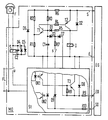
- a telephone set F is indicated, which is usually. is connected to the two wires of a telephone line FL.
- a changeover contact u which belongs to a relay U to be considered in more detail below.
- a relay S in the connection in question, to which two diodes D4, D5 connected in anti-parallel to one another and a capacitor C2 are connected in parallel.
- This arrangement thus corresponds entirely to the connection arrangement via which the telephone set is connected to a telephone line in accordance with the main patent.
- the relay S is energized when the telephone set F has effectively connected to the telephone line FL, which is the case with a normal telephone connection.
- a terminal device EG is indicated in the drawing, which may be a data delivery / data recording device which, for example, can output or record data signals at 1200 bit / s.
- This terminal EG is connected to a series of inputs and outputs to be considered in more detail with a modem MO which can be connected to the telephone line FL via the switch contact U already mentioned. The modem MO is then with the Telephone line FL is effectively connected when the changeover contact u assumes its other switch position, not shown in the drawing.
- the modem MO includes a timer shown in the upper part of the drawing and a control circuit St. indicated in the lower part of the drawing.
- the timing element is connected to the terminal EG via a switch-on signal line labeled S and via a grounding or return line labeled E. Between these two lines S and E occurs the above-mentioned switch-on signal, which is emitted by the terminal EG when this terminal EG tries to establish a connection to the telephone line FL via the modem MO.
- the mentioned switch-on signal can occur at a level between 4V and 7V.
- the control circuit St is connected to the terminal EG via a transmission data line SD carrying transmission data, via a reception data line ED receiving data and via the aforementioned earthing line E.
- the timing element shown in the upper part of the drawing contains an integrating element consisting of a capacitor C1 and a resistor R3 in series therewith and a resistance voltage divider consisting of the resistors R1 and R2.
- the mentioned integrator and the mentioned resistance voltage divider are directly connected to each other at the outer ends. Via a protective resistor R6, the integrating element and the resistor economy divider are thus acted upon together with the switch-on signal which can be output by the terminal EG.
- the base of a transistor T1 is connected to the connection point between the resistor R3 and the capacitor C1 of the aforementioned integrator npn conductivity type.
- This transistor has its emitter connected at the junction of the resistors R1 and R2 forming the resistance voltage divider.
- the transistor T1 in question thus acts as a comparator which compares the voltage across the capacitor C1 with the voltage present at the junction of the two resistors R1, R2. If, in the present case, the voltage across capacitor C1 is higher (positive) than the voltage across the connection point of the two resistors R1, R2 by the base-emitter voltage drop of approximately 0.7 V of transistor T1, transistor T1 comes out of it normally non-conductive state in the conductive state.
- the transistor T1 is connected with its collector via a protective resistor R4 to the base of a further transistor T2, which is of the pnp conductivity type.
- This transistor T2 has its emitter on the switch-on signal line S.
- the collector of the transistor T2 is connected to the base of the transistor T1 via a resistor R5 and a diode D1.
- the collector of the transistor T2 is connected to the line E via the relay U already mentioned above.
- the diode D1 it should also be noted that this is polarized so that the part of the collector current of the transistor T2 flowing through the resistor R5 can flow into the base of the transistor T1.
- the previously explained circuit arrangement comprising the two transistors T1 and T2 is a self-holding circuit.
- the two transistors T1 and T2 are initially in the non-conductive state and the transistor T1 is subsequently brought into the conductive state - in that the base voltage of the transistor T1 is 0.7 V higher than the emitter voltage of the transistor T1 - the transistor T2 also becomes conductive.
- the transistor T1 is controlled to be more conductive.
- the circuit in question remains in this state even if the level of the switch-on signal (S) subsequently decreases.
- the circuit in question can only be safely returned to its initial state in that the switch-on signal (S) is switched off completely.
- the g for the respective timer eh ö- in power transistor T2 is a Zener diode D2 connected in parallel and that the above-mentioned integrating circuit and the resistor voltage divider also mentioned a diode D6 is connected in parallel.
- These two diodes D2 and D6 serve to protect the timing element in question from being destroyed by an activation signal (S) which occurs with the wrong polarity.
- the zener diode also serves to protect the transistor T2 from inductive shutdown voltage peaks from the relay U.
- this always energizes the relay U after a predetermined, fixed period of time when a switch-on signal (S) occurs. Any fluctuations or different levels in the relevant switch-on signal (S), which may occur at a level between 4V and 7V, have no effect on the relevant time period, since both the integrator and the resistance voltage divider mentioned together by the relevant switch-on signal be applied and since the transistor T1 acting as a comparator is controlled by these two circuit parts.
- the capacitor C1 of the integrating element is connected in parallel with a series circuit which consists of a diode D3, a resistor R7 and a switch s, which is formed by the contact of the above-mentioned relay S.
- the relevant contact s is closed when the relay S is energized.
- This relay S is then energized when the telephone set F is operatively connected to the telephone line FL.
- the diodes D4 and D5 lying parallel to the relay S protect the relay S against overload.
- the capacitor C2 reduces the insertion loss of the relevant parallel circuit, consisting of the relay S and the diodes D4, D5.
- switch or contact s which is to a certain extent a switch that can be actuated by an occupancy signal - from the telephone set F, is in the present case via the resistor R7 and a decoupling diode D7 and via a resistor R9 with the received data line ED connected to the terminal EG.
- the diode D7 can also be connected directly to the contact or to the base of a transistor T3 belonging to the control circuit St, which is of the pnp conductivity type.
- the collector of transistor T3 is with
- the emitter of transistor T3 is connected to said receive data line ED via resistor R9.
- the emitter-collector path of the transistor T3 is connected in parallel with a diode D8, which serves as a so-called reverse polarity protection and which protects the transistor T3 from being destroyed by voltages occurring with the wrong polarity.
- the base and emitter of transistor T3 are connected to one another by a resistor R8.
- the base of the transistor T3 is connected to the transistor of an optocoupler Ok1, the transistor of which may otherwise be connected to the ground line E.
- the LED belonging to the optocoupler Ok1 will be operatively connected to the telephone line FL if the modem MO is connected to this telephone line.
- control circuit St also includes an optocoupler Ok2, the light-emitting diode of which is connected to the transmit data line SD of the terminal EG and to the ground line E via a protective resistor R10.
- the light-emitting diode in question is connected in parallel with a diode D9 which serves to protect against polarity reversal.
- the collector-emitter path of the transistor belonging to the optocoupler Ok2 can be connected to the telephone line FL if the modem MO is connected to this telephone line.
- the transistor T1 could be connected with its emitter to the integrating element and with its base to the resistance voltage divider in deviation from the conditions explained.
Landscapes
- Engineering & Computer Science (AREA)
- Computer Networks & Wireless Communication (AREA)
- Signal Processing (AREA)
- Telephonic Communication Services (AREA)
- Communication Control (AREA)
Priority Applications (1)
| Application Number | Priority Date | Filing Date | Title |
|---|---|---|---|
| AT83108387T ATE35884T1 (de) | 1982-08-30 | 1983-08-25 | Schaltungsanordnung zum anschalten eines modems an eine fernsprechleitung. |
Applications Claiming Priority (2)
| Application Number | Priority Date | Filing Date | Title |
|---|---|---|---|
| DE19823232240 DE3232240A1 (de) | 1982-08-30 | 1982-08-30 | Schaltungsanordnung zum anschalten eines modems an eine fernsprechleitung |
| DE3232240 | 1982-08-30 |
Publications (3)
| Publication Number | Publication Date |
|---|---|
| EP0102064A2 true EP0102064A2 (fr) | 1984-03-07 |
| EP0102064A3 EP0102064A3 (en) | 1986-10-08 |
| EP0102064B1 EP0102064B1 (fr) | 1988-07-20 |
Family
ID=6172068
Family Applications (1)
| Application Number | Title | Priority Date | Filing Date |
|---|---|---|---|
| EP83108387A Expired EP0102064B1 (fr) | 1982-08-30 | 1983-08-25 | Montage de circuit pour connecter un modem à une ligne téléphonique |
Country Status (3)
| Country | Link |
|---|---|
| EP (1) | EP0102064B1 (fr) |
| AT (1) | ATE35884T1 (fr) |
| DE (2) | DE3232240A1 (fr) |
Family Cites Families (2)
| Publication number | Priority date | Publication date | Assignee | Title |
|---|---|---|---|---|
| GB1124492A (en) * | 1965-04-23 | 1968-08-21 | Reyrolle A & Co Ltd | Improvements relating to electric timing circuits |
| DE2931435C2 (de) * | 1979-08-02 | 1981-10-01 | Siemens AG, 1000 Berlin und 8000 München | Schaltungsanordnung zum Anschalten eines Modems an eine Fernsprechleitung |
-
1982
- 1982-08-30 DE DE19823232240 patent/DE3232240A1/de not_active Withdrawn
-
1983
- 1983-08-25 AT AT83108387T patent/ATE35884T1/de active
- 1983-08-25 DE DE8383108387T patent/DE3377446D1/de not_active Expired
- 1983-08-25 EP EP83108387A patent/EP0102064B1/fr not_active Expired
Also Published As
| Publication number | Publication date |
|---|---|
| EP0102064B1 (fr) | 1988-07-20 |
| ATE35884T1 (de) | 1988-08-15 |
| EP0102064A3 (en) | 1986-10-08 |
| DE3232240A1 (de) | 1984-03-01 |
| DE3377446D1 (en) | 1988-08-25 |
Similar Documents
| Publication | Publication Date | Title |
|---|---|---|
| DE69004085T2 (de) | Schutzanordnung mit automatischer wiedereinstellung für eine teilnehmerschaltung. | |
| DE3632746C2 (de) | Schaltungsanordnung zur Erzeugung einer Wechselspannung | |
| DE3876852T2 (de) | Schutzanordnung fuer eine fernsprech-teilnehmerschnittstellen-schaltung. | |
| DE3332427T1 (de) | In einem Gleichstromverteilungssystem enthaltener elektronischer Stromunterbrecher | |
| DE1301841B (de) | Schaltungsanordnung zur Auswertung des Schleifenzustandes und zur Unterscheidung vonSchleifenwiderstaenden einer Fernmelde-, insbesondere Fernsprechleitung | |
| DE68905055T2 (de) | Binaer-ternaer-umsetzer zur kombination von zwei binaer-signalen. | |
| DE3686947T2 (de) | Geraet und methode zum schutz einer elektrischen schaltung. | |
| EP0141971B1 (fr) | Dispositif pour l'alimentation, selon les besoins, par le réseau ou à distance d'un poste d'abonné | |
| DE69216370T2 (de) | Auslösesteuervorrichtung für einen Schalter | |
| DE3230250C2 (de) | Teilnehmerschaltung für den Anschluß einer zweiadrigen Teilnehmerleitung an eine Fernmelde-, insbesondere Fernsprechanlage | |
| EP0409327B1 (fr) | Dispositif d'alimentation de courant avec circuit de surveillance | |
| DE2809905C2 (de) | Relais-Halteschaltung | |
| EP0102064B1 (fr) | Montage de circuit pour connecter un modem à une ligne téléphonique | |
| DE19532677B4 (de) | Überwachungsschaltung für wenigstens eine Versorgungsspannung | |
| DE2715609B2 (de) | Fenster-Diskriminatorschaltung | |
| DE2522957A1 (de) | Schaltungsanordnung fuer ueber ihre anschlussleitungen gespeiste teilnehmerstationen mit impulstastwahl in fernmelde-, insbesondere fernsprechanlagen | |
| DE69210742T2 (de) | Steuerungs und Ausgangsschutzverfahren, insbesondere für eine programmierbare Steuerung | |
| DE3812733C3 (de) | Kurzschluß-Schutzschaltung | |
| DE3248355A1 (de) | Schaltungsanordnung zur abgabe von waehlimpulsen in einer fernmelde-, insbesondere fernsprechanlage | |
| DE2603263A1 (de) | Treiberschaltung mit ueberlastungsschutz | |
| DE2251879C3 (de) | Schaltungsanordnung zur Abtastung von Fernsprechleitungen | |
| DE2931435C2 (de) | Schaltungsanordnung zum Anschalten eines Modems an eine Fernsprechleitung | |
| DE4420216C2 (de) | Anordnung zum Übertragen von Binärsignalen über eine Signalleitung | |
| EP1005709A1 (fr) | Dispositif protecteur pour courant de fuite | |
| EP0702445A1 (fr) | Disjoncteur de protection à courants de défaut avec circuit de stockage d'énergie |
Legal Events
| Date | Code | Title | Description |
|---|---|---|---|
| PUAI | Public reference made under article 153(3) epc to a published international application that has entered the european phase |
Free format text: ORIGINAL CODE: 0009012 |
|
| AK | Designated contracting states |
Designated state(s): AT CH DE LI NL |
|
| 17P | Request for examination filed |
Effective date: 19841217 |
|
| PUAL | Search report despatched |
Free format text: ORIGINAL CODE: 0009013 |
|
| AK | Designated contracting states |
Kind code of ref document: A3 Designated state(s): AT CH DE LI NL |
|
| 17Q | First examination report despatched |
Effective date: 19870202 |
|
| R17C | First examination report despatched (corrected) |
Effective date: 19870702 |
|
| GRAA | (expected) grant |
Free format text: ORIGINAL CODE: 0009210 |
|
| AK | Designated contracting states |
Kind code of ref document: B1 Designated state(s): AT CH DE LI NL |
|
| REF | Corresponds to: |
Ref document number: 35884 Country of ref document: AT Date of ref document: 19880815 Kind code of ref document: T |
|
| PG25 | Lapsed in a contracting state [announced via postgrant information from national office to epo] |
Ref country code: AT Effective date: 19880825 |
|
| REF | Corresponds to: |
Ref document number: 3377446 Country of ref document: DE Date of ref document: 19880825 |
|
| PG25 | Lapsed in a contracting state [announced via postgrant information from national office to epo] |
Ref country code: LI Effective date: 19880831 Ref country code: CH Effective date: 19880831 |
|
| PG25 | Lapsed in a contracting state [announced via postgrant information from national office to epo] |
Ref country code: NL Effective date: 19890301 |
|
| NLV4 | Nl: lapsed or anulled due to non-payment of the annual fee | ||
| REG | Reference to a national code |
Ref country code: CH Ref legal event code: PL |
|
| PLBE | No opposition filed within time limit |
Free format text: ORIGINAL CODE: 0009261 |
|
| STAA | Information on the status of an ep patent application or granted ep patent |
Free format text: STATUS: NO OPPOSITION FILED WITHIN TIME LIMIT |
|
| 26N | No opposition filed | ||
| PG25 | Lapsed in a contracting state [announced via postgrant information from national office to epo] |
Ref country code: DE Effective date: 19900501 |