EP0102183A2 - Zündung von Entladungslampen - Google Patents
Zündung von Entladungslampen Download PDFInfo
- Publication number
- EP0102183A2 EP0102183A2 EP83304251A EP83304251A EP0102183A2 EP 0102183 A2 EP0102183 A2 EP 0102183A2 EP 83304251 A EP83304251 A EP 83304251A EP 83304251 A EP83304251 A EP 83304251A EP 0102183 A2 EP0102183 A2 EP 0102183A2
- Authority
- EP
- European Patent Office
- Prior art keywords
- voltage
- lamp
- circuit
- switch
- pulse
- Prior art date
- Legal status (The legal status is an assumption and is not a legal conclusion. Google has not performed a legal analysis and makes no representation as to the accuracy of the status listed.)
- Granted
Links
- 239000007858 starting material Substances 0.000 claims abstract description 27
- 239000004065 semiconductor Substances 0.000 claims abstract description 10
- 239000003990 capacitor Substances 0.000 claims description 33
- 230000001419 dependent effect Effects 0.000 claims description 24
- 238000013016 damping Methods 0.000 claims description 3
- 230000003247 decreasing effect Effects 0.000 claims description 2
- 230000001747 exhibiting effect Effects 0.000 claims description 2
- 230000000694 effects Effects 0.000 description 11
- 238000004519 manufacturing process Methods 0.000 description 8
- 230000001960 triggered effect Effects 0.000 description 8
- 230000000630 rising effect Effects 0.000 description 7
- 229910052743 krypton Inorganic materials 0.000 description 6
- DNNSSWSSYDEUBZ-UHFFFAOYSA-N krypton atom Chemical compound [Kr] DNNSSWSSYDEUBZ-UHFFFAOYSA-N 0.000 description 6
- 230000015556 catabolic process Effects 0.000 description 5
- 230000002238 attenuated effect Effects 0.000 description 4
- 238000010438 heat treatment Methods 0.000 description 4
- 230000007935 neutral effect Effects 0.000 description 4
- 230000002441 reversible effect Effects 0.000 description 4
- 230000000750 progressive effect Effects 0.000 description 3
- XKRFYHLGVUSROY-UHFFFAOYSA-N Argon Chemical compound [Ar] XKRFYHLGVUSROY-UHFFFAOYSA-N 0.000 description 2
- 230000001186 cumulative effect Effects 0.000 description 2
- 230000007547 defect Effects 0.000 description 2
- 230000003111 delayed effect Effects 0.000 description 2
- 238000011161 development Methods 0.000 description 2
- XUIMIQQOPSSXEZ-UHFFFAOYSA-N Silicon Chemical compound [Si] XUIMIQQOPSSXEZ-UHFFFAOYSA-N 0.000 description 1
- 229910052786 argon Inorganic materials 0.000 description 1
- 230000001174 ascending effect Effects 0.000 description 1
- 238000012937 correction Methods 0.000 description 1
- 238000013461 design Methods 0.000 description 1
- 238000007599 discharging Methods 0.000 description 1
- 238000003780 insertion Methods 0.000 description 1
- 230000037431 insertion Effects 0.000 description 1
- 238000009434 installation Methods 0.000 description 1
- 230000002250 progressing effect Effects 0.000 description 1
- 229910052710 silicon Inorganic materials 0.000 description 1
- 239000010703 silicon Substances 0.000 description 1
- 239000000126 substance Substances 0.000 description 1
- 230000000007 visual effect Effects 0.000 description 1
Images


Classifications
-
- H—ELECTRICITY
- H05—ELECTRIC TECHNIQUES NOT OTHERWISE PROVIDED FOR
- H05B—ELECTRIC HEATING; ELECTRIC LIGHT SOURCES NOT OTHERWISE PROVIDED FOR; CIRCUIT ARRANGEMENTS FOR ELECTRIC LIGHT SOURCES, IN GENERAL
- H05B41/00—Circuit arrangements or apparatus for igniting or operating discharge lamps
- H05B41/02—Details
- H05B41/04—Starting switches
- H05B41/042—Starting switches using semiconductor devices
- H05B41/044—Starting switches using semiconductor devices for lamp provided with pre-heating electrodes
- H05B41/046—Starting switches using semiconductor devices for lamp provided with pre-heating electrodes using controlled semiconductor devices
Definitions
- This invention relates to the starting of discharge lamps by electronic starter circuits, in particular such circuits employing the pulse producing properties of a non-linear dielectric element, which will be referred to hereinafter as a voltage dependent capacitor or VDC.
- Patent Application No. 2 035 287A also illustrates a circuit utilising a voltage dependent capacitor to provide an ignition pulse for a discharge lamp. This utilises the fact that as the saturation voltage is exceeded the capacitance falls rapidly and current through the element falls sharply to zero. If the capacitor is connected in series with a lamp ballast inductance, the sudden saturation of the capacitor can give rise to a high di for ignition of the lamp. dt
- circuits of the said Patent Application suffers from certain defects for some purposes. Further circuits employing a voltage dependent capacitor are disclosed in European Patent Application publication No. 0 048 137 Al, which is more particularly directed to circuits for lamp ignition. In addition to disclosing several circuits stated to be conventional, the said European Patent Application discloses circuits, starting at Figure 8, in which a voltage dependent capacitor is connected in parallel with a semiconductor switch and in series with a second semiconductor switch. One of these switches serves to control the flow of preheating current to the lamp electrodes and the other to provide a path for the current through the VDC when it suddenly reduces to generate the large ignition pulses required.
- a discharge lamp starter circuit having two starter input terminals for connecting to the cathodes of a discharge lamp to receive a cyclically varying voltage supplied through both the lamp cathodes and a choke ballast, the starter circuit including a semiconductor switch, a voltage dependent capacitor, capable of providing a voltage pulse substantially in excess of twice the peak of said cyclically varying voltage in response to a voltage pulse higher than the saturation voltage thereof and a circuit arranged to connect said switch across said input terminals in one polarity in one part of a starting cycle to pass preheating current through said cathodes and to connect said switch in the opposite polarity and in series with said voltage dependent capacitor in another part of said starting cycle to provide an ignition voltage pulse across said lamp.
- the circuit arranged to connect said switch across said input terminals may be a diode steering circuit.
- Circuit elements may be introduced into the path including the voltage dependent capacitor to vary its operation.
- Such elements include means to prevent the voltage dependent capacitor charging until a predetermined voltage has been reached or means for damping a pulse of one polarity resulting from saturation.
- the semiconductor switch may be a self triggering breakback device, otherwise a trigger circuit will be included.
- a circuit may be provided to make the trigger circuit responsive to the cyclically varying voltage selectively in preference to short duration voltage pulses thereby being suitable for starting lamps exhibiting high re-ignition voltages, for example T8 Krypton filled lamps.
- the circuits are preferably arranged to reduce or prevent stressing of the voltage dependent capacitor when the lamp is running.
- the starter includes a circuit requiring a progressively increasing trigger voltage and thereby providing progressively decreasing preheat current pulses.
- the circuit may be arranged to provide ignition pulses of progressively increasing magnitude, at least after a predetermined portion of a starting period and up to the end of a second predetermined portion.
- the present invention provides starter circuits which are believed to be more efficient than prior art circuits and advantageous at least by providing the capability of provision of more advanced features.
- the circuit of the invention uses the realisation that in prior art circuits, in which the disadvantages due to flows of-charging and -discharging currents through a voltage dependent capacitor have been recognised, for example European Patent Application 0 048 137, page 11, the solution has involved the provision of two semiconductor switches with consequent increase in complexity and expense. The two switches are performing different functions but at different stages in the operation of the circuit.
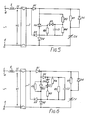
- the circuit is shown in a simplified form in Figure 3 in which it is associated with a fluorescent lamp 1, which may be a T12 lamp, of the hot cathode type having two cathodes 2 and 3.
- a fluorescent lamp 1 which may be a T12 lamp
- One side 2a of cathode 2 is connected to one terminal 4 of a mains supply through an inductor or choke ballast 5 and one side, 3a, of the other cathode is connected directly to the other terminal 6 of the mains supply.
- the starter circuit is connected across the other terminals 2b and 3b of the cathodes.
- the circuit comprises a series connection of a diode D, and a voltage dependent capacitor Cy, in parallel with two diodes D 2 and D 3 in series opposition.
- switch S Connected between the junction of the diode D 1 and C V and the junction between the two diodes D 2 and D 3 is a unidirectional switch S having in parallel therewith a trigger circuit 7.
- switch S will be a semiconductor switch and circuit 7, which will be described in more detail with reference to later Figures, is for operation of the switch.
- the invention does, however, also embrace the use of a self-triggering break back device for which a trigger circuit is not required.
- the diodes D 1 to D 3 comprise a diode steering arrangement which allows the switch S to provide the functions in relation to capacitor C V and the lamp 1, performed in prior art circuits by two different switches.
- switch S There are two principal modes for triggering of switch S. The first is for it to be triggered on before V CV reaches V CS (the saturation voltage). The second, which applies to a circuit such as Figure 3 in which there are no elements in series with capacitor C v , is that V CV reaches V CS before S has triggered whereupon its impedance rises and V CV is the cause of S being triggered on.
- the circuit allows scope for introducing elements in the C V path to vary the operation.
- means can be used to prevent C V charging until a predetermined voltage has been reached, for example by a zener diode.
- an element such as a resistor may be used to influence the charging of C v and hence the degree of saturation achieved at a given applied voltage.
- the inclusion of such a resistor may also reduce the choke di/dt and hence the magnitude of any positive pulse resulting from the saturation voltage being reached. This may be associated with a diode poled to shunt it when an ignition pulse is provided.
- the magnitude of the voltage across the switch rises towards a theoretical maximum (depending on the 'Q' factor) of peak mains voltage, the ascending pulse being characteristic of the ringing of the choke inductance (L) with stray circuit capacitance (C S ) in the system.
- the voltage across the lamp falls from zero towards minus twice peak mains voltage (again depending on 'Q') and D, and D 2 are biassed off.
- the switch S has been arranged to perform the two functions of passing the preheat current for one polarity and passing the ignition pulse with the opposite polarity at the lamp but current flow being in the same direction at the switch and trigger circuit.
- V CV will invariably reach +V CS before the switch trigger voltage is reached.
- the resulting positive pulse will cause the switch S to be triggered whereupon the pulse is immediately truncated via D1.
- This voltage is then superimposed on the next negative half cycle lamp voltage presented to the trigger circuit resulting in a cumulative voltage approaching twice the lamp peak (for example, for a 4ft, 40W, T12 lamp, about 400V). If, as is typical for the same lamp, the fixed trigger voltage of the trigger circuit is set to 300V, the switch S will close, -V CS will be exceeded and a negative pulse produced, the pulse being similarly attenuated by the lamp as before.
- FIG 4 shows one practical embodiment of the circuit of Figure 3 employing a fixed voltage trigger but including means for overcoming the voltage-doubling problem just described.
- the unidirectional switch S is a silicon control rectifier TH1.
- the fixed voltage trigger network comprises a zener diode ZD1 and a resistor R 2 in conventional manner and TH1 is shunted by a resistor R 3 .
- TH1 is shunted by a resistor R 3 .
- diode D 4 and and resistor R 1 in parallel with each other.
- the resistor R 1 is however of sufficient value to allow V CV to be carried above + V CS without producing a significant positive pulse as indicated hereinbefore to be an option.
- R 1 has a damping effect on any C V current attenuation thus reducing the resulting pulse.
- D 4 provides a low impedance path across R 1 to enable a larger pulse to be passed.
- the negative ringing pulse, in the ballast and stray capacitances, is presented to the trigger network via D 4 and D 31 causing ZD 1 to trigger TH1 into conduction.
- C V charges to the negative pulse height and is then discharged via D, and R 1 as the pulse falls and the ringing current reverses.
- the circuit of Figure 3 in its practical form as shown in Figure 4 is suitable for starting many discharge (fluorescent) lamps, in particular the well known T12 argon filled lamp.
- fluorescent lamp now enjoying increasing use is the T8 Krypton filled lamp which has a higher ignition voltage than earlier lamps.
- the circuit of Figure 4 is not suitable for starting lamps such as T8 Krypton filled lamps having high reignition voltages.
- the circuit of Figure 4 provides a solution to the voltage doubling problem in fixed voltage trigger circuits as described hereinbefore .
- the relatively low fixed trigger voltage renders the circuit unsuitable for lamps having reignition voltages approaching 300V on 240 RMS supplies (or 275V on 220V supplies). With such lamps, not only would the VDC C V be stressed but cathode heating would continue to flow due to triggering of the switch S on positive half cycles of the lamp running waveform.
- Figure 5 shows a further development of the circuit of this invention which overcomes this problem and is therefore suitable for T8 Krypton filled lamps.
- the trigger network of Figure 4 is replaced with the network of Diac D S , resistor R 2 and capacitor C 1 and resistors R 3 and D 4 .
- This is in fact a known type of RC delayed thyristor switch circuit which in this arrangement discriminates against the short duration large re-ignition pulses.
- Resistors R 3 and R 4 serve in place of R 3 in Figure 4 to discharge Cy.
- the use of a diac trigger requires some means for suppressing positive pulses to protect the switching device and resistor R 1 is included for that purpose.
- Figure 6 represents a further development which is preferred to that of Figure 5 since it includes a progressive trigger switch of the type described and claimed in British Patent No. 1 602 456 which provides a progressively increasing trigger voltage and discontinuation of triggering if the lamp does not start, as described in that Patent: This feature ensures that the VDC is not continually stressed if the lamp does not start.
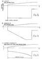
- Figure 7a shows the envelope of the lamp voltage waveform when attempting to start a lamp using the progressive trigger of British Patent No. 1 602 456 and in fact corresponds substantially to Figure 5a of that patent. It will be seen that the positive envelope is rising past the point at which the lamp would normally strike, to a maximum at the point at which the switch ceases to trigger, this rise corresponds to the rise in the trigger voltage as the charge on capacitor C1 ( Figure 6) increases up to ignition.
- the negative voltage envelope which is the envelope of the ignition pulses themselves, is of constant amplitude until ignition occurs or until the switch ceases to trigger.
- this invention allows a progression of the amplitude of the ignition pulses themselves. This is achieved by an appropriate selection of the value of R 1 . It has been noted in relation to Figures 4 and 5 that R controls the charging of Cy during starting (and also reduces stressing in the run mode). In the arrangement of Figure 6, R 1 can be selected to control Cy charging so that the ratio of C VH to C VL is gradually increased. Thus if the positive trigger level at the cathode of D 1 progressively increases, the positive voltage across C V over R 1 also progressively increases, for example from below + V CS to above + V CS . As Cy is carried progressively towards and into positive saturation the C v negative pulse amplitude progressively increases due to the hysteresis effect.
- R1 The value of R1 must be low enough to ensure that ignition pulses of sufficient magnitude are ultimately produced and high enough to
- the envelope of Fig. 7c is also preferable in respect of lamp life by reducing cathode damage and the resulting "end blackening" associated with lamp ionization before the cathodes have reached emission temperature.
- the circuit of Figure 6 does suffer from one minor defect in that the value of R 1 required to produce the preferred progression of Figure 7C is so large that C v is not fully positively biassed within the starting cycle and maximum negative pulses are not realised.
- a preferred circuit for production purposes is therefore that shown in Figure 8.
- the lamp current and lamp voltage waveforms for this circuit are shown in Figure 9 and in that Figure the leading edge of the negative ignition pulse is characterised by the ringing of the ballast choke and the VDC in its low capacitance state (the VDC is connected across the lamp via TH1).
- a first part of a voltage rise (determined by the breakdown voltage of a zener diode ZD 2 , typically 200V) of the trailing edge is, however, characteristic of ballast/stray capacitance ringing after which the VDC begins to discharge, remaining clamped at 200V below the voltage across the starter and once more influencing the pulse shape.
- C v is biassed fully to + V CS and therefore the maximum change of capacitance is achieved to produce the maximum negative going ignition pulses.
- R is a comparatively low resistance value. Therefore in the region C-D the negative ignition pulse amplitude is constant at its maximum value. As shown in Figure 9, at D if the lamp has not started, as it would usually have done as shown by the inset, then the circuit ceases to operate.
- the voltage dependent capacitor C V also produces positive pulses at fixed times (when + V CS is reached) and consequently the preheat pulses are then initiated at the same conduction angle and cease to progress.
- the voltage dependent capacitor C v is again forward biassed via diode D 1 and consequently it pulses.
- the pulse then obtained is not limited by conduction of TH1 and may reach damaging amplitudes.
- a zener diode ZD4 is added. This acts in conjunction with ZD3 to limit the magnitude of pulses from C V .
- the voltage on C v is not limited to V ZD3 .
- the voltage on C V reaches a peak defined by ( V ZD3 + V ZD4 - V ZD2 ).
- This voltage subsequently discharges towards peak mains voltage ( V ZD3 ) through R 1 , ZD2, D 5 , R 4 , ZD3 , D3 and the choke on the next negative half cycle although the actual voltage attained depends essentially on the time constant C V R 4.
- R 4 The value of R 4 is such that -V CS is not to be exceeded and on the subsequent positive half cycle, no pulse is produced and C V charges to a voltage of + peak mains voltage (V ZD2 ).
- Full pulse production is arranged to be delayed (by the choice of ZD2) until the trigger voltage has progressed above the lamp running voltage.
- the lamp will invariably start on a negative ignition pulse and the subsequent positive voltage applied to the starter (that is the lamp running voltage), whilst remaining below the trigger voltage, will still allow +V CS to be exceeded.
- the consequent pulse is, however, attenuated by the lamp and TH1 is not triggered, the VDC thereby remaining charged to the peak lamp running voltage minus V ZD2 .
- C v is recharged on the next positive half cycle but no pulse is produced since -V CS has not previously been exceeded. The cycle will then continue throughout the period of lamp operation.
- ZD3 and ZD4 perform no function if the lamp strikes before the end of the available starting period.
- D 4 and R 6 may be omitted but in that case the value of R 1 should be closer to that given above for R 6.
- references to positive and negative voltages are with respect to neutral mains so that all of the circuits described so far produce negative pulses. It is, however, believed that for circuits of this type superior lamp starting is obtained from positive ignition pulses for reasons which are not entirely understood.
- FIG 10 shows a circuit which is in all essential respects the same as that of Figure 8, and is suitable for starting T8 Krypton filled lamps, but produces positive ignition pulses.
- PFC power factor correction
Landscapes
- Circuit Arrangements For Discharge Lamps (AREA)
- Pyrane Compounds (AREA)
- Pharmaceuticals Containing Other Organic And Inorganic Compounds (AREA)
Priority Applications (1)
| Application Number | Priority Date | Filing Date | Title |
|---|---|---|---|
| AT83304251T ATE32823T1 (de) | 1982-08-05 | 1983-07-22 | Zuendung von entladungslampen. |
Applications Claiming Priority (2)
| Application Number | Priority Date | Filing Date | Title |
|---|---|---|---|
| GB8222651 | 1982-08-05 | ||
| GB8222651 | 1982-08-05 |
Publications (3)
| Publication Number | Publication Date |
|---|---|
| EP0102183A2 true EP0102183A2 (de) | 1984-03-07 |
| EP0102183A3 EP0102183A3 (en) | 1985-01-23 |
| EP0102183B1 EP0102183B1 (de) | 1988-03-02 |
Family
ID=10532143
Family Applications (1)
| Application Number | Title | Priority Date | Filing Date |
|---|---|---|---|
| EP83304251A Expired EP0102183B1 (de) | 1982-08-05 | 1983-07-22 | Zündung von Entladungslampen |
Country Status (6)
| Country | Link |
|---|---|
| EP (1) | EP0102183B1 (de) |
| AT (1) | ATE32823T1 (de) |
| AU (1) | AU559657B2 (de) |
| DE (1) | DE3375874D1 (de) |
| NZ (1) | NZ205154A (de) |
| ZA (1) | ZA835513B (de) |
Cited By (1)
| Publication number | Priority date | Publication date | Assignee | Title |
|---|---|---|---|---|
| FR2550043A1 (fr) * | 1983-07-28 | 1985-02-01 | Diehl Gmbh & Co | Montage pour amorcer des lampes a substance luminescente et en regler la luminosite |
Family Cites Families (2)
| Publication number | Priority date | Publication date | Assignee | Title |
|---|---|---|---|---|
| DE2949074A1 (de) * | 1979-12-06 | 1981-06-11 | Philips Patentverwaltung Gmbh, 2000 Hamburg | Spannungsimpulsgenerator zum zuenden einer gasentladungslampe |
| JPS5750797A (en) * | 1980-09-11 | 1982-03-25 | Mitsubishi Electric Corp | Device for firing discharge lamp |
-
1983
- 1983-07-22 DE DE8383304251T patent/DE3375874D1/de not_active Expired
- 1983-07-22 AT AT83304251T patent/ATE32823T1/de not_active IP Right Cessation
- 1983-07-22 EP EP83304251A patent/EP0102183B1/de not_active Expired
- 1983-07-28 ZA ZA835513A patent/ZA835513B/xx unknown
- 1983-08-02 AU AU17522/83A patent/AU559657B2/en not_active Ceased
- 1983-08-04 NZ NZ205154A patent/NZ205154A/en unknown
Cited By (1)
| Publication number | Priority date | Publication date | Assignee | Title |
|---|---|---|---|---|
| FR2550043A1 (fr) * | 1983-07-28 | 1985-02-01 | Diehl Gmbh & Co | Montage pour amorcer des lampes a substance luminescente et en regler la luminosite |
Also Published As
| Publication number | Publication date |
|---|---|
| AU1752283A (en) | 1984-02-09 |
| AU559657B2 (en) | 1987-03-19 |
| ZA835513B (en) | 1984-06-27 |
| EP0102183B1 (de) | 1988-03-02 |
| EP0102183A3 (en) | 1985-01-23 |
| DE3375874D1 (en) | 1988-04-07 |
| NZ205154A (en) | 1986-12-05 |
| ATE32823T1 (de) | 1988-03-15 |
Similar Documents
| Publication | Publication Date | Title |
|---|---|---|
| US4937501A (en) | Circuit arrangement for starting a high-pressure gas discharge lamp | |
| US5010274A (en) | Starter circuits for discharge lamps | |
| EP0948245A2 (de) | Dimmbares elektronisches Vorschaltgerät mit komplementären elektronischen Schaltern | |
| US4629944A (en) | Starter circuit for a fluorescent tube lamp | |
| US5055742A (en) | Gas discharge lamp dimming system | |
| KR100281373B1 (ko) | 고강도 방전 램프용 전자 밸러스트 | |
| US4959593A (en) | Two-lead igniter for HID lamps | |
| CA1262256A (en) | Dc/ac converter for igniting and feeding a gas and/or vapour discharge lamp | |
| EP0671869B1 (de) | Vorschaltgerät für eine Lampe | |
| US6188180B1 (en) | Ignition circuit for automotive high intensity discharge lamps | |
| EP0048137B1 (de) | Zündschaltung für eine Entladungsröhre | |
| EP0102183B1 (de) | Zündung von Entladungslampen | |
| US5572093A (en) | Regulation of hot restrike pulse intensity and repetition | |
| US4539513A (en) | Circuit arrangement for starting and operating a high-pressure gas discharge lamp | |
| US5994846A (en) | Buck converter switching scheme | |
| US4227118A (en) | Circuits for operating electric discharge lamps | |
| US5514938A (en) | D.C. ciruit for starting high pressure discharge lamp | |
| US5084655A (en) | Circuit arrangement suitable for igniting a high-pressure discharge lamp | |
| US4893061A (en) | Switching arrangement | |
| CN1137608C (zh) | 电路装置 | |
| JPS6251194A (ja) | ガス放電灯点弧及び作動回路配置 | |
| US6137241A (en) | Starting switch circuit for a fluorescent lamp | |
| US5781424A (en) | Static converter for an incandescent lamp having a delayed start | |
| EP0011410B1 (de) | Elektronische Starterschaltungen für Entladungslampen | |
| US6621237B2 (en) | Gas-discharge lamp lighting apparatus with optimized circuit configuration |
Legal Events
| Date | Code | Title | Description |
|---|---|---|---|
| PUAI | Public reference made under article 153(3) epc to a published international application that has entered the european phase |
Free format text: ORIGINAL CODE: 0009012 |
|
| AK | Designated contracting states |
Designated state(s): AT CH DE FR GB IT LI NL |
|
| PUAL | Search report despatched |
Free format text: ORIGINAL CODE: 0009013 |
|
| AK | Designated contracting states |
Designated state(s): AT CH DE FR GB IT LI NL |
|
| 17P | Request for examination filed |
Effective date: 19850227 |
|
| 17Q | First examination report despatched |
Effective date: 19861009 |
|
| ITF | It: translation for a ep patent filed | ||
| GRAA | (expected) grant |
Free format text: ORIGINAL CODE: 0009210 |
|
| AK | Designated contracting states |
Kind code of ref document: B1 Designated state(s): AT CH DE FR GB IT LI NL |
|
| REF | Corresponds to: |
Ref document number: 32823 Country of ref document: AT Date of ref document: 19880315 Kind code of ref document: T |
|
| REF | Corresponds to: |
Ref document number: 3375874 Country of ref document: DE Date of ref document: 19880407 |
|
| ET | Fr: translation filed | ||
| PLBE | No opposition filed within time limit |
Free format text: ORIGINAL CODE: 0009261 |
|
| STAA | Information on the status of an ep patent application or granted ep patent |
Free format text: STATUS: NO OPPOSITION FILED WITHIN TIME LIMIT |
|
| 26N | No opposition filed | ||
| ITTA | It: last paid annual fee | ||
| PGFP | Annual fee paid to national office [announced via postgrant information from national office to epo] |
Ref country code: GB Payment date: 19920727 Year of fee payment: 10 |
|
| PGFP | Annual fee paid to national office [announced via postgrant information from national office to epo] |
Ref country code: CH Payment date: 19920728 Year of fee payment: 10 |
|
| PGFP | Annual fee paid to national office [announced via postgrant information from national office to epo] |
Ref country code: FR Payment date: 19920730 Year of fee payment: 10 Ref country code: AT Payment date: 19920730 Year of fee payment: 10 |
|
| PGFP | Annual fee paid to national office [announced via postgrant information from national office to epo] |
Ref country code: NL Payment date: 19920731 Year of fee payment: 10 |
|
| PGFP | Annual fee paid to national office [announced via postgrant information from national office to epo] |
Ref country code: DE Payment date: 19920925 Year of fee payment: 10 |
|
| PG25 | Lapsed in a contracting state [announced via postgrant information from national office to epo] |
Ref country code: GB Effective date: 19930722 Ref country code: AT Effective date: 19930722 |
|
| PG25 | Lapsed in a contracting state [announced via postgrant information from national office to epo] |
Ref country code: LI Effective date: 19930731 Ref country code: CH Effective date: 19930731 |
|
| PG25 | Lapsed in a contracting state [announced via postgrant information from national office to epo] |
Ref country code: NL Effective date: 19940201 |
|
| NLV4 | Nl: lapsed or anulled due to non-payment of the annual fee | ||
| GBPC | Gb: european patent ceased through non-payment of renewal fee |
Effective date: 19930722 |
|
| PG25 | Lapsed in a contracting state [announced via postgrant information from national office to epo] |
Ref country code: FR Effective date: 19940331 |
|
| REG | Reference to a national code |
Ref country code: CH Ref legal event code: PL |
|
| PG25 | Lapsed in a contracting state [announced via postgrant information from national office to epo] |
Ref country code: DE Effective date: 19940401 |
|
| REG | Reference to a national code |
Ref country code: FR Ref legal event code: ST |