EP0102452A2 - Cellule multiplexable à cristal liquide - Google Patents
Cellule multiplexable à cristal liquide Download PDFInfo
- Publication number
- EP0102452A2 EP0102452A2 EP83104882A EP83104882A EP0102452A2 EP 0102452 A2 EP0102452 A2 EP 0102452A2 EP 83104882 A EP83104882 A EP 83104882A EP 83104882 A EP83104882 A EP 83104882A EP 0102452 A2 EP0102452 A2 EP 0102452A2
- Authority
- EP
- European Patent Office
- Prior art keywords
- liquid crystal
- crystal cell
- cell according
- insulation layer
- data line
- Prior art date
- Legal status (The legal status is an assumption and is not a legal conclusion. Google has not performed a legal analysis and makes no representation as to the accuracy of the status listed.)
- Granted
Links
Images


Classifications
-
- G—PHYSICS
- G02—OPTICS
- G02F—OPTICAL DEVICES OR ARRANGEMENTS FOR THE CONTROL OF LIGHT BY MODIFICATION OF THE OPTICAL PROPERTIES OF THE MEDIA OF THE ELEMENTS INVOLVED THEREIN; NON-LINEAR OPTICS; FREQUENCY-CHANGING OF LIGHT; OPTICAL LOGIC ELEMENTS; OPTICAL ANALOGUE/DIGITAL CONVERTERS
- G02F1/00—Devices or arrangements for the control of the intensity, colour, phase, polarisation or direction of light arriving from an independent light source, e.g. switching, gating or modulating; Non-linear optics
- G02F1/01—Devices or arrangements for the control of the intensity, colour, phase, polarisation or direction of light arriving from an independent light source, e.g. switching, gating or modulating; Non-linear optics for the control of the intensity, phase, polarisation or colour
- G02F1/13—Devices or arrangements for the control of the intensity, colour, phase, polarisation or direction of light arriving from an independent light source, e.g. switching, gating or modulating; Non-linear optics for the control of the intensity, phase, polarisation or colour based on liquid crystals, e.g. single liquid crystal display cells
- G02F1/133—Constructional arrangements; Operation of liquid crystal cells; Circuit arrangements
- G02F1/1333—Constructional arrangements; Manufacturing methods
- G02F1/1335—Structural association of cells with optical devices, e.g. polarisers or reflectors
- G02F1/133502—Antiglare, refractive index matching layers
-
- G—PHYSICS
- G02—OPTICS
- G02F—OPTICAL DEVICES OR ARRANGEMENTS FOR THE CONTROL OF LIGHT BY MODIFICATION OF THE OPTICAL PROPERTIES OF THE MEDIA OF THE ELEMENTS INVOLVED THEREIN; NON-LINEAR OPTICS; FREQUENCY-CHANGING OF LIGHT; OPTICAL LOGIC ELEMENTS; OPTICAL ANALOGUE/DIGITAL CONVERTERS
- G02F1/00—Devices or arrangements for the control of the intensity, colour, phase, polarisation or direction of light arriving from an independent light source, e.g. switching, gating or modulating; Non-linear optics
- G02F1/01—Devices or arrangements for the control of the intensity, colour, phase, polarisation or direction of light arriving from an independent light source, e.g. switching, gating or modulating; Non-linear optics for the control of the intensity, phase, polarisation or colour
- G02F1/13—Devices or arrangements for the control of the intensity, colour, phase, polarisation or direction of light arriving from an independent light source, e.g. switching, gating or modulating; Non-linear optics for the control of the intensity, phase, polarisation or colour based on liquid crystals, e.g. single liquid crystal display cells
- G02F1/133—Constructional arrangements; Operation of liquid crystal cells; Circuit arrangements
- G02F1/136—Liquid crystal cells structurally associated with a semi-conducting layer or substrate, e.g. cells forming part of an integrated circuit
- G02F1/1362—Active matrix addressed cells
- G02F1/1365—Active matrix addressed cells in which the switching element is a two-electrode device
Definitions
- the invention relates to a multiplexable liquid crystal cell with two spaced substrates, which form a cell space filled with liquid crystal substance between them, with strip electrodes arranged on the one side on the cell space side and image electrodes arranged on the other side of the cell space side, opposite the strip electrodes
- Metal-insulator-metal elements are also connected to data lines arranged on the substrate.
- this liquid crystal cell not only requires a large number of process steps, but is also complex due to the anodic construction of the insulating layer.
- This object is achieved in that an insulation layer is arranged on the image electrode arranged on the substrate, which in turn carries a connection contact leading to the data line.
- the number of production steps can be reduced, since the metal-insulator-metal element (MIM element) consists of the image electrode, the insulation layer and the connecting contact, and thus, contrary to the known liquid crystal cell, the image electrode is at the same time part of the MIM element .
- MIM element metal-insulator-metal element
- the fine structure of the picture electrodes enabled the Can be produced without significant adjustment problems with respect to the data lines and connection contacts, allows good multiplexability, which leads to a better optical contrast and thus a better detectability of the information.
- the insulation layer can be transparent so that the legibility of the information is not impaired. If the insulation layer completely covers the image electrode, this layer fulfills both the function as part of the MIM element and the function as an insulator for the image electrode. Such an insulator to be applied in a separate operation is therefore not necessary.
- this insulation layer has a refractive index that lies between the refractive index of the liquid crystal substance and the refractive index of the transparent picture electrode, it fulfills a third function in that it leads to better and more high-contrast detectability by antireflection of the picture electrodes.
- the insulation layer can have a refractive index between 1.5 and 2.0, preferably 1.8.
- a further function can be fulfilled by the insulation layer in that it possesses a property orienting the adjacent liquid crystal substance and is therefore still an orientation layer.
- the data lines and / or the connection contact consist of a transparent material, for example indium tin oxide, they cannot disturb the good appearance of the display.
- the data is preferred line and the connection contact applied in one operation.
- an antireflection coating covers the image electrode and / or the data line and / or the connection contact, then none of the covered parts can emit a reflection that impairs the contrast and readability.
- This antireflection coating can furthermore have a property orienting the adjacent liquid crystal substance and an insulating property and thus fulfill a multiple function.
- the data line is arranged parallel to the strip electrodes opposite the space between two strip electrodes, then the data line and a strip electrode are not closely opposed, so that the field between the data line and the strip electrode is only very small.
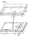
- the liquid crystal cells shown in the figures consist of an upper substrate 1 made of glass, which carries a controllable strip electrode 2.
- the lower substrate 3, which is also made of glass, carries an image electrode 4.
- a data line 5 is arranged on the substrate 3, and a connection contact 6 leading to the image electrode 4 is arranged in one piece therewith.
- An insulation layer 7 is arranged between the connection contact 6, which partially overlaps the image electrode 4, and the image electrode 4, which is only approximately the size of the connection contact 6 in FIGS covered substrate 3 covers.
- the liquid crystal substance (not shown), which is symbolized by a helix 8, is arranged between the substrates, which are shown explosively at a distance from one another in FIGS. 1 and 2.
- the image electrode 4 and the data lines 5 and connecting contacts 6 forming an application layer are made of indium tin oxide and are therefore transparent.
- the insulation layer 7 is also transparent, so that none of these components can adversely affect the appearance of the display.
- the insulation layer 7 has a refractive index that lies between the refractive index of the liquid crystal substance and the refractive index of the transparent image electrode and also has properties that orientate the adjacent liquid crystal substance, it performs several functions and otherwise saves additional operations for the production of layers that fulfill these functions.
Landscapes
- Physics & Mathematics (AREA)
- Nonlinear Science (AREA)
- Mathematical Physics (AREA)
- Chemical & Material Sciences (AREA)
- Crystallography & Structural Chemistry (AREA)
- General Physics & Mathematics (AREA)
- Optics & Photonics (AREA)
- Engineering & Computer Science (AREA)
- Microelectronics & Electronic Packaging (AREA)
- Liquid Crystal (AREA)
- Devices For Indicating Variable Information By Combining Individual Elements (AREA)
Applications Claiming Priority (2)
| Application Number | Priority Date | Filing Date | Title |
|---|---|---|---|
| DE3229584 | 1982-08-07 | ||
| DE3229584A DE3229584A1 (de) | 1982-08-07 | 1982-08-07 | Multiplexbare fluessigkristallzelle |
Publications (3)
| Publication Number | Publication Date |
|---|---|
| EP0102452A2 true EP0102452A2 (fr) | 1984-03-14 |
| EP0102452A3 EP0102452A3 (en) | 1986-12-03 |
| EP0102452B1 EP0102452B1 (fr) | 1990-01-17 |
Family
ID=6170417
Family Applications (1)
| Application Number | Title | Priority Date | Filing Date |
|---|---|---|---|
| EP83104882A Expired - Lifetime EP0102452B1 (fr) | 1982-08-07 | 1983-05-18 | Cellule multiplexable à cristal liquide |
Country Status (6)
| Country | Link |
|---|---|
| US (1) | US4572615A (fr) |
| EP (1) | EP0102452B1 (fr) |
| JP (1) | JPS5934515A (fr) |
| AU (1) | AU557215B2 (fr) |
| BR (1) | BR8304105A (fr) |
| DE (2) | DE3229584A1 (fr) |
Cited By (5)
| Publication number | Priority date | Publication date | Assignee | Title |
|---|---|---|---|---|
| EP0176734A1 (fr) * | 1984-10-05 | 1986-04-09 | VDO Adolf Schindling AG | Cellule à cristaux liquides multiplexable |
| EP0208078A1 (fr) * | 1985-07-05 | 1987-01-14 | VDO Adolf Schindling AG | Cellule à cristal liquide |
| EP0182484A3 (en) * | 1984-10-16 | 1987-09-02 | Seiko Instruments & Electronics Ltd. | Liquid crystal display device |
| EP0246945A1 (fr) * | 1986-05-20 | 1987-11-25 | Thomson-Csf | Ecran de visualisation électrooptique, et procédé de réalisation |
| EP0187223A3 (fr) * | 1984-12-20 | 1988-06-29 | VDO Adolf Schindling AG | Cellule à cristal liquide pouvant être adressée par multiplexage |
Families Citing this family (14)
| Publication number | Priority date | Publication date | Assignee | Title |
|---|---|---|---|---|
| US4666252A (en) * | 1984-06-29 | 1987-05-19 | Energy Conversion Devices, Inc. | High yield liquid crystal display and method of making same |
| JPH0617957B2 (ja) * | 1985-05-15 | 1994-03-09 | セイコー電子工業株式会社 | 液晶表示装置 |
| US4828370A (en) * | 1985-10-04 | 1989-05-09 | Seiko Instruments & Electronics Ltd. | Switching element with nonlinear resistive, nonstoichiometric material |
| JP2816549B2 (ja) * | 1986-10-22 | 1998-10-27 | セイコーインスツルメンツ株式会社 | 電気光学装置 |
| JP2605382B2 (ja) * | 1987-12-18 | 1997-04-30 | セイコーエプソン株式会社 | アクティブマトリクス基板の製造方法 |
| US5282069A (en) * | 1987-12-23 | 1994-01-25 | Seiko Epson Corporation | Active device and active matrix display having ferroelectric layer as active layer |
| US5268777A (en) * | 1987-12-23 | 1993-12-07 | Seiko Epson Corporation | Driving method of active matrix display having ferroelectric layer as active layer |
| US5225821A (en) * | 1988-12-22 | 1993-07-06 | Seiko Epson Corporation | Method for driving an active matrix display and active matrix display |
| JP2757207B2 (ja) * | 1989-05-24 | 1998-05-25 | 株式会社リコー | 液晶表示装置 |
| DE4302913A1 (de) * | 1993-02-03 | 1994-08-04 | Bosch Gmbh Robert | Flüssigkristallelement mit Linseneigenschaften |
| US5978056A (en) * | 1995-10-15 | 1999-11-02 | Victor Company Of Japan, Ltd | Reflection-type display apparatus having antireflection films |
| US6282010B1 (en) * | 1998-05-14 | 2001-08-28 | Texas Instruments Incorporated | Anti-reflective coatings for spatial light modulators |
| US7187487B2 (en) * | 2004-07-30 | 2007-03-06 | Hewlett-Packard Development Company, L.P. | Light modulator with a light-absorbing layer |
| CN100483235C (zh) * | 2006-12-04 | 2009-04-29 | 中芯国际集成电路制造(上海)有限公司 | 硅基液晶显示器单元及其形成方法 |
Family Cites Families (8)
| Publication number | Priority date | Publication date | Assignee | Title |
|---|---|---|---|---|
| US3736047A (en) * | 1971-08-13 | 1973-05-29 | Optical Coating Laboratory Inc | Liquid crystal display device with internal anti-reflection casting |
| DE2827258A1 (de) * | 1978-06-21 | 1980-01-03 | Siemens Ag | Elektrooptische anzeigevorrichtung, insbesondere fluessigkristallanzeige |
| CA1121489A (fr) * | 1979-05-30 | 1982-04-06 | Northern Telecom Limited | Afficheurs a cristal liquide controles par dispositif metal-isolant-metal |
| US4431271A (en) * | 1979-09-06 | 1984-02-14 | Canon Kabushiki Kaisha | Display device with a thin film transistor and storage condenser |
| JPS5941168B2 (ja) * | 1979-10-25 | 1984-10-05 | セイコーエプソン株式会社 | 表示パネルの構造 |
| DE2949837A1 (de) * | 1979-12-12 | 1981-06-19 | Vdo Adolf Schindling Ag, 6000 Frankfurt | Fluessigkristallzelle |
| FR2505070B1 (fr) * | 1981-01-16 | 1986-04-04 | Suwa Seikosha Kk | Dispositif non lineaire pour un panneau d'affichage a cristaux liquides et procede de fabrication d'un tel panneau d'affichage |
| JPS57122477A (en) * | 1981-01-22 | 1982-07-30 | Suwa Seikosha Kk | Liquid crystal display device |
-
1982
- 1982-08-07 DE DE3229584A patent/DE3229584A1/de not_active Ceased
-
1983
- 1983-05-18 DE DE8383104882T patent/DE3381121D1/de not_active Expired - Lifetime
- 1983-05-18 EP EP83104882A patent/EP0102452B1/fr not_active Expired - Lifetime
- 1983-07-06 AU AU16611/83A patent/AU557215B2/en not_active Ceased
- 1983-07-14 JP JP58127022A patent/JPS5934515A/ja active Pending
- 1983-08-01 BR BR8304105A patent/BR8304105A/pt not_active IP Right Cessation
- 1983-08-03 US US06/520,063 patent/US4572615A/en not_active Expired - Fee Related
Cited By (6)
| Publication number | Priority date | Publication date | Assignee | Title |
|---|---|---|---|---|
| EP0176734A1 (fr) * | 1984-10-05 | 1986-04-09 | VDO Adolf Schindling AG | Cellule à cristaux liquides multiplexable |
| EP0182484A3 (en) * | 1984-10-16 | 1987-09-02 | Seiko Instruments & Electronics Ltd. | Liquid crystal display device |
| EP0187223A3 (fr) * | 1984-12-20 | 1988-06-29 | VDO Adolf Schindling AG | Cellule à cristal liquide pouvant être adressée par multiplexage |
| EP0208078A1 (fr) * | 1985-07-05 | 1987-01-14 | VDO Adolf Schindling AG | Cellule à cristal liquide |
| EP0246945A1 (fr) * | 1986-05-20 | 1987-11-25 | Thomson-Csf | Ecran de visualisation électrooptique, et procédé de réalisation |
| FR2599171A1 (fr) * | 1986-05-20 | 1987-11-27 | Thomson Csf | Ecran de visualisation electrooptique et procede de realisation |
Also Published As
| Publication number | Publication date |
|---|---|
| EP0102452A3 (en) | 1986-12-03 |
| AU1661183A (en) | 1984-02-09 |
| US4572615A (en) | 1986-02-25 |
| DE3229584A1 (de) | 1984-02-09 |
| DE3381121D1 (de) | 1990-02-22 |
| EP0102452B1 (fr) | 1990-01-17 |
| BR8304105A (pt) | 1984-04-24 |
| JPS5934515A (ja) | 1984-02-24 |
| AU557215B2 (en) | 1986-12-11 |
Similar Documents
| Publication | Publication Date | Title |
|---|---|---|
| EP0102452B1 (fr) | Cellule multiplexable à cristal liquide | |
| DE68920130T2 (de) | Flüssigkristallanzeige mit aktiver Matrix. | |
| DE3153620C2 (fr) | ||
| DE69131987T2 (de) | Flüssigkristall-Anzeigevorrichtung | |
| DE19828591B4 (de) | Flüssigkristallanzeige mit einem hohen Öffnungsverhältnis und ein Verfahren zur Herstellung derselben | |
| DE69032893T2 (de) | Werkstoff für elektrische Leiter, Elektronikagerät welches diesen verwendet und Flüssig-Kristall-Anzeige | |
| DE3783870T2 (de) | Transistor-gesteuerter elektrooptischer anzeigeschirm und verfahren zu seiner herstellung. | |
| DE3686351T2 (de) | Fluessigkristallanzeigevorrichtung. | |
| DE3852617T2 (de) | Farb-Flüssigkristall-Anzeigevorrichtung und ihr Herstellungsverfahren. | |
| DE69110563T2 (de) | Flüssigkristall-Anzeigevorrichtung. | |
| DE19906815B4 (de) | Flüssigkristallanzeige und Verfahren zur Herstellung derselben | |
| DE3750573T2 (de) | Dünnschicht-Transistoranordnung für Anzeigetafel aus Flüssigkristallen. | |
| DE69017262T2 (de) | Aktiv-Matrix-Anzeigevorrichtung und Verfahren zu ihrer Herstellung. | |
| DE3889395T2 (de) | Verfahren zur Trennung eines kurzgeschlossenen Teiles zwischen oberen und unteren Elektroden einer Flüssigkristallanzeigetafel und Verfahren zur Fertigung einer Flüssigkristallanzeigetafel unter Verwendung dieses Verfahrens. | |
| DE3201122A1 (de) | Nicht-linearer widerstand und verfahren zur herstellung eines solche verwendenden matrix-fk-anzeigefeldes | |
| DE69015100T2 (de) | Elektroden auf einem Montagesubstrat und Flüssigkristallanzeigevorrichtung, die dieses enthält. | |
| DE3886198T2 (de) | Flüssigkristall-Anzeigevorrichtung. | |
| DE4318028A1 (de) | Flüssigkristallanzeigeeinrichtung und Verfahren zu deren Herstellung | |
| DE3714164A1 (de) | Fluessigkristallanzeige | |
| DE19746055A1 (de) | Flüssigkristallanzeige und Herstellungsverfahren dafür | |
| DE69010701T2 (de) | Methode zur Herstellung von aktiven Matrixanzeigevorrichtungen. | |
| DE19710248A1 (de) | Flüssigkristallanzeige mit aktiver Matrix und Herstellungsverfahren dafür | |
| DE69326132T2 (de) | Flüssigkristall-Anzeigetafel mit aktiver Matrix und Verfahren zu ihrer Herstellung | |
| DE3545400A1 (de) | Elektrochrome vorrichtung | |
| EP0391024A1 (fr) | Circuit pour dispositif d'affichage |
Legal Events
| Date | Code | Title | Description |
|---|---|---|---|
| PUAI | Public reference made under article 153(3) epc to a published international application that has entered the european phase |
Free format text: ORIGINAL CODE: 0009012 |
|
| AK | Designated contracting states |
Designated state(s): DE FR GB IT SE |
|
| PUAL | Search report despatched |
Free format text: ORIGINAL CODE: 0009013 |
|
| AK | Designated contracting states |
Kind code of ref document: A3 Designated state(s): DE FR GB IT SE |
|
| 17P | Request for examination filed |
Effective date: 19861103 |
|
| 17Q | First examination report despatched |
Effective date: 19880428 |
|
| GRAA | (expected) grant |
Free format text: ORIGINAL CODE: 0009210 |
|
| AK | Designated contracting states |
Kind code of ref document: B1 Designated state(s): DE FR GB IT SE |
|
| ET | Fr: translation filed | ||
| REF | Corresponds to: |
Ref document number: 3381121 Country of ref document: DE Date of ref document: 19900222 |
|
| ITF | It: translation for a ep patent filed | ||
| GBT | Gb: translation of ep patent filed (gb section 77(6)(a)/1977) | ||
| PLBE | No opposition filed within time limit |
Free format text: ORIGINAL CODE: 0009261 |
|
| STAA | Information on the status of an ep patent application or granted ep patent |
Free format text: STATUS: NO OPPOSITION FILED WITHIN TIME LIMIT |
|
| 26N | No opposition filed | ||
| PGFP | Annual fee paid to national office [announced via postgrant information from national office to epo] |
Ref country code: DE Payment date: 19910418 Year of fee payment: 9 |
|
| PGFP | Annual fee paid to national office [announced via postgrant information from national office to epo] |
Ref country code: SE Payment date: 19910422 Year of fee payment: 9 |
|
| PGFP | Annual fee paid to national office [announced via postgrant information from national office to epo] |
Ref country code: FR Payment date: 19910506 Year of fee payment: 9 |
|
| PGFP | Annual fee paid to national office [announced via postgrant information from national office to epo] |
Ref country code: GB Payment date: 19910508 Year of fee payment: 9 |
|
| ITTA | It: last paid annual fee | ||
| PG25 | Lapsed in a contracting state [announced via postgrant information from national office to epo] |
Ref country code: GB Effective date: 19920518 |
|
| PG25 | Lapsed in a contracting state [announced via postgrant information from national office to epo] |
Ref country code: SE Effective date: 19920519 |
|
| GBPC | Gb: european patent ceased through non-payment of renewal fee |
Effective date: 19920518 |
|
| PG25 | Lapsed in a contracting state [announced via postgrant information from national office to epo] |
Ref country code: FR Effective date: 19930129 |
|
| PG25 | Lapsed in a contracting state [announced via postgrant information from national office to epo] |
Ref country code: DE Effective date: 19930202 |
|
| REG | Reference to a national code |
Ref country code: FR Ref legal event code: ST |
|
| EUG | Se: european patent has lapsed |
Ref document number: 83104882.2 Effective date: 19921204 |