EP0102608A2 - Circuit d'expansion pour signaux numériques - Google Patents
Circuit d'expansion pour signaux numériques Download PDFInfo
- Publication number
- EP0102608A2 EP0102608A2 EP83108496A EP83108496A EP0102608A2 EP 0102608 A2 EP0102608 A2 EP 0102608A2 EP 83108496 A EP83108496 A EP 83108496A EP 83108496 A EP83108496 A EP 83108496A EP 0102608 A2 EP0102608 A2 EP 0102608A2
- Authority
- EP
- European Patent Office
- Prior art keywords
- signal
- bits
- data
- compressed
- bit
- Prior art date
- Legal status (The legal status is an assumption and is not a legal conclusion. Google has not performed a legal analysis and makes no representation as to the accuracy of the status listed.)
- Withdrawn
Links
- 238000007906 compression Methods 0.000 description 27
- 230000006835 compression Effects 0.000 description 27
- 230000005236 sound signal Effects 0.000 description 19
- 238000013144 data compression Methods 0.000 description 13
- 238000010586 diagram Methods 0.000 description 8
- 230000005540 biological transmission Effects 0.000 description 6
- 238000005070 sampling Methods 0.000 description 3
- 230000010354 integration Effects 0.000 description 2
- 238000013139 quantization Methods 0.000 description 2
- 239000008186 active pharmaceutical agent Substances 0.000 description 1
- 238000006243 chemical reaction Methods 0.000 description 1
- 238000000034 method Methods 0.000 description 1
Images


Classifications
-
- H—ELECTRICITY
- H03—ELECTRONIC CIRCUITRY
- H03M—CODING; DECODING; CODE CONVERSION IN GENERAL
- H03M7/00—Conversion of a code where information is represented by a given sequence or number of digits to a code where the same, similar or subset of information is represented by a different sequence or number of digits
- H03M7/30—Compression; Expansion; Suppression of unnecessary data, e.g. redundancy reduction
- H03M7/50—Conversion to or from non-linear codes, e.g. companding
-
- H—ELECTRICITY
- H03—ELECTRONIC CIRCUITRY
- H03G—CONTROL OF AMPLIFICATION
- H03G7/00—Volume compression or expansion in amplifiers
- H03G7/007—Volume compression or expansion in amplifiers of digital or coded signals
-
- H—ELECTRICITY
- H04—ELECTRIC COMMUNICATION TECHNIQUE
- H04B—TRANSMISSION
- H04B14/00—Transmission systems not characterised by the medium used for transmission
- H04B14/02—Transmission systems not characterised by the medium used for transmission characterised by the use of pulse modulation
- H04B14/04—Transmission systems not characterised by the medium used for transmission characterised by the use of pulse modulation using pulse code modulation
- H04B14/046—Systems or methods for reducing noise or bandwidth
- H04B14/048—Non linear compression or expansion
Definitions
- the present invention relates to an expansion circuit for expanding the amplitude of compressed signal to its original value, and more particularly to an expansion circuit for digital signals which is used in the case where an analog signal is converted into a PCM signal, the amount of data of the PCM signal is compressed, the PCM signal thus compressed is transmitted or recorded in a recording medium, and the amount of data of the compressed ' PCM signal is expanded to an original amount to demodulate the transmitted or recorded signal.
- an analog signal such as an audio signal
- a sampled value thus obtained is quantized and digitized to be converted into a PCM signal
- the PCM signal is transmitted through a transmission line
- the amount of data of the PCM signal is compressed and the PCM signal thus compressed is transmitted if the transmission capacity of the transmission line is insufficient.
- one sampled value expressed by a 10-bit PCM signal is compressed into an 8-bit signal, which is transmitted through the transmission line.
- the audio signal is converted into a PCM signal and the PCM signal thus obtained is recorded in a portion of a video track on the magnetic tape.
- the video signal is recorded on the magnetic tape obliquely with respect to the longitudinal direction thereof by means of a plurality of rotating video heads.
- the magnetic recording/reproducing device is of helical scanning type.
- About four fifths of the total length of the video track is used to record the video signal by the video heads, and the remaining one fifth of the video track is used to record the PCM signal obtained from the audio signal, by the video heads.
- the amount of data of the PCM signal recorded in the video track is compressed, since that portion of the video track which is used to record the PCM signal, is small in length. That is, the audio signal which is an analog signal, is sampled, the sampled value thus obtained is converted into a 10-bit digital signal, and the 10-bit digital signal is compressed into an 8-bit signal, which is recorded in the video track.
- a compression circuit operates in such a manner that the 10-bit PCM signal is left uncompressed when the amplitude of the audio signal is small, and is compressed when the amplitude of the audio signal is large.
- the amplitude of the audio signal is small, noise is readily observed and therefore the PCM signal is left uncompressed.
- the amplitude of the audio signal is large, one or more lower bits of the PCM signal are cut off to compress the data thereof. That is, when the amplitude of the audio signal is small, eight lower bits of a 10-bit PCM signal indicating the above amplitude are taken out to be delivered.
- the audio signal takes a high level, one or two lower bits of a 10-bit PCM signal indicating the ampltidue of the audio signal are cut off, and eight lower bits of the 9-bit or 8-bit signal thus obtained are taken out to be delivered.
- the PCM signal was compressed, are added to the compressed PCM signal at the position following the least significant bit of the compressed PCM signal and further one or more bits are added to the compressed PCM signal at an upper bit portion thereof, to convert the compressed PCM signal into the 10-bit PCM signal.
- a numerical value indicated by one or more bits which were cut off when the" PCM signal was compressed cannot be estimated when the compressed PCM signal is expanded. Therefore, a numerical value "0" is generally given to one or more bits which are added to the compressed PCM signal at the position following the least significant bit of the compressed PCM signal. Accordingly, it is impossible to reproduce the original PCM signal by expanding the compressed PCM signal, and therefore a distortion is generated in an output signal obtained by expanding the compressed signal.
- an expansion circuit for digital signal in which a digital signal whose data has been compressed, is supplied to bit- adding means, one or more bits corresponding to the number of bits which were cut off when a digital signal indicating a sampled value of an analog signal and including a plurality of bits was compressed, are added to the compressed digital signal at the position following the least significant bit of the compressed digital signal to form an expanded digital signal, and a numerical value which is about one half the largest one of numerical values represented by one or more bits thus added, is given to one or more added bits, to reduce the distortion of the expanded digital signal.
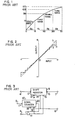
- Fig. 1 shows the compression characteristic of a nonlinear compression circuit.
- the abscissa indicates the signal level of input signal, and the ordinate the signal level of compressed output signal.
- An input signal applied to the compression circuit includes positive and negative signals, and the compression characteristic for the positive signal is similar to that for the negative signal. Therefore, only the compression characteristic for the positive signal is shown in Fig. 1.
- the input signal is a 10-bit digital signal indicating a sampled value which is obtained by sampling an analog signal. A bit group which includes ten bits to indicate one sampled value, is called one block.
- the compressed output signal from the compression circuit is an 8-bit digital signal, by way of example.
- a maximum numerical value expressed by a 10-bit digital signal is 1024 in decimal notation.
- both positive and negative parts of the audio signal are expressed by the digital signal. Accordingly, when the audio signal takes zero level, the signal level is expressed by "0" in decimal notation.
- the positive level is expressed by a numerical value of 1 to 511 in decimal notation.
- a negative signal level of the audio signal is expressed by a numerical value of -1 to -512 in decimal notation.
- an input signal whose signal level is expressed by decimal number within a range from 0 to 511 is used in the compression characteristic shown in Fig. 1.
- An actual compression circuit is applied with a 10-bit digital signal which indicates a binary number corresponding to the above-mentioned decimal number.
- the compression characteristic shown in Fig. 1 is divided into four ranges, that is, the zero-th range a 0 in which the signal level of input signal takes a value of 0 to 15, the first range a 1 in which the signal level of input signal takes a value of 16 to 63, the second range a 2 in which the signal level of input signal takes a value of 64 to 319, and the third range a3 in which the signal level of input signal takes a value of 320 to 511.
- the compression circuit When the signal level of input signal lies within the zero-th range a 0 , the compression circuit does not compress the input signal. Thus, the input signal is left uncompressed, and only eight lower bits of the input signal (namely, the 10-bit signal) are taken out to be delivered.
- an input signal whose signal level lies within a range from 0 to 15, namely, from (0000000000) to (0000001111), is taken out as it is, and only eight lower bits of the 10-bit input signal are taken out.
- the output signal indicates a binary number of (OODOOOOO) to (00001111).
- the signal level of input signal lies in the first range a 1 , that is, takes a value of 16 to 63
- the least significant bit of a 10-bit input signal is cut off, and an offset value 8 is added to the input signal thus processed.
- the signal level of output signal takes a value of 16 to 39.
- a 10-bit PCM signal (0000010000) indicating a binary number corresponding to a decimal number 16
- the least significant bit of the 10-bit PCM signal is cut off, and thus a binary number (000001000) is obtained.
- This binary number corresponds to a decimal number 8. That is, the numerical number 16 is reduced to the numerical number 8.
- the numerical number 8 thus obtained cannot be descriminated from a numerical value 8 in the zero-th range a 0 . Therefore, the offset value 8 is added to the binary number (000001000), and only eight lower bits of the binary number thus obtained are taken out. In this manner, an 8-bit binary number (00010000) corresponding to a decimal number 16 is outputted as a compressed signal. Similarly, a 10-bit signal indicating a binary number corresponding to a decimal number 63 is expressed by (0000111111), and the least significant bit of this 10-bit signal is cut off. Thus, a binary number (000011111) is obtained which corresponds to a decimal number 31.
- the offset value 8 is added to the decimal number 31, and thus a numerical value 39, that is, an 8-bit signal (00100111) is outputted.
- the compression circuit cuts off two lower bits of a 10-bit input signal to compress the input signal. That is, two lower bits of a 10-bit PCM signal (0001000000) indicating a binary number corresponding to a decimal number 64 are cut off, and thus an 8-bit signal (00010000) is obtained. This signal corresponds to a decimal number 16.
- An offset value 24 is added to the 8-bit signal, and thus an 8-bit signal (00101000) is outputted.
- the compression circuit cuts off three lower bits of a 10-bit input signal to compress the input signal. That is, three lower bits of a 10-bit PCM signal (0101000000) indicating a binary number corresponding to a decimal number 320 are cut off, and thus a 7-bit signal (0101000) is obtained. This signal corresponds to a decimal number 40. An offset value 64 is added to the 7-bit signal, and then an 8-bit signal (01101000) corresponding to a decimal number 104 is outputted.
- a compression circuit for performing such operations includes a shift register for cutting off one or more lower bits of a 10-bit input signal, a register for storing therein offset values, and an adder for adding one of the offset values to the content of the shift register.
- the compression characteristic shown in Fig. 1 can be expressed by a quantization characteristic shown in Fig. 2.
- the output signal of the compression circuit is given by a stepwise characteristic 3 shown in Fig. 2.
- the output signal is finely quantized in a region where the signal level of input signal is low, and is coarsely quantized in a region where the signal level of input signal is high.
- Fig. 3 is a block diagram showing a conventional expansion circuit for expanding the compressed data of PCM signal.
- reference numeral 9 designates a shift register, 10 a down counter, and 11 an AND circuit.
- compressed data and a range signal are supplied to a data input terminal 4 and a range-signal input terminal 5, respectively.
- a reset-signal input terminal 8 is supplied with a reset signal for starting a data expanding operation.
- the reset signal is applied to a load terminal 14 of the shift register 9 and to a load terminal 18 of the down counter 10.
- the shift register 9 is loaded with the compressed data applied to parallel input terminals 12 of the shift register 9, and the down counter 10 is loaded with the range signal applied to an input terminal 17 of the down counter 10.
- a clock signal supplied to a clock input terminal 6 is applied through the AND circuit 11 to a clock input terminal 15 of the shift register 9 and to a clock input terminal 19 of the down counter 10.
- the clock signal is supplied to the shift register 9 and down counter 10
- the input data loaded in the shift register 9 is shifted, and the down counter 10 counts down the range signal loaded therein.
- the expansion circuit shown in Fig. 3 can be used when a PCM signal applied thereto accompanies a range signal.
- the expansion circuit is used in the case where compressed data is transmitted together with a range signal [0], [1], [2] or [3] indicating which of the zero-th, first, second and third ranges has been used, in compressing the data of PCM signal in accordance with the compression characteristic shown in Fig. 1.
- a transmitted PCM signal is divided into data indicating the amplitude of audio signal and a range signal.
- the data and range signal are supplied to the data input terminal 4 and range-signal input terminal 5, respectively.
- the data of a PCM signal is compressed in such a manner that one or more lower bits of an input signal are cut off when the signal level of the input signal is high. Accordingly, in the expansion circuit, the data of a transmitted PCM signal is shifted by a predetermined number of bits, and one or more bits corresponding to the number of bits cut off in a compression circuit are added to the shifted data at the position following the least significant bit of the shifted data, to expand the data of the transmitted PCM signal.
- the range signal indicates the number of bits added to the shifted data. In other words, the range signal indicates which of the ranges a 0 to a3 has been used in compressing the data of PCM signal, that is, how many bits have been cut off in data compression.
- the PCM signal supplied to the input terminal 4 is applied to the parallel input terminals 12 of the shift register 9, and one block of the PCM signal loaded from the parallel input terminals 12 in the shift register 9, for example, compressed 8-bit data is shifted in the direction toward the most significant bit of the shift register, by one bit in synchronism with the clock signal applied to the clock input terminal 15, each time the clock signal is applied to the terminal 15.
- the range signal supplied to the input terminal 5 is applied to the input terminal 17 of the down counter 10.
- the range signal indicates the number of bits cut off in data compression, as mentioned previously.
- the down counter 10 counts down the range signal loaded therein, in response to the clock signal applied to the input terminal 19.
- the range signal indicates the number of cut off bits (namely, 3), and the down counter 10 counts down the numerical value 3 on the basis of the clock signal.
- the shift register 9 shifts the whole data loaded therein in the direction toward the most significant bit of the register 9, in synchronism with the clock signal. Accordingly, when the range signal loaded in the down counter 10 is made equal to zero by three clock pulses, the whole data in the shift register 9 is shifted in the direction toward the most significant bit thereof by three bits, and thus a 3-bit data area is formed following the least significant bit of the shifted data.
- the PCM signal outputted from the output terminal 7 is applied to a subtractor (not shown), in which the offset value having been added in the compression is subtracted from the PCM signal.
- Fig. 4 shows a few examples of data expansion performed in the case where a 10-bit PCM signal has been compressed into a 7-bit signal.
- reference numeral 21 designates one block of compressed data
- 22 expanded data corresponding to the case where the zero-th range a 0 is used to obtain the compressed data
- 23 expanded data corresponding to the case where the first range a 1 is used for data compression
- 24 expanded data corresponding to the case where the second range a 2 is used for data compression
- 25 expanded data corresponding to the case where the third range a3 is used for data compression.
- Each of these expanded data is one block of data.
- the most significant bit D 6 of the compressed data 21 is a sign bit for indicating one of positive and negative signs, and is used in the most significant bit of each expanded data, as it is.
- the remaining bits of the compressed data namely, six bits DO to D 5 are shifted in accordance with one of the ranges a l to a3.
- the data 22 corresponds to the case where the zero-th range is used for data
- the data bits D 0 to D 5 are not subjected to bit shift, but only the sign bit D 6 is moved to the most significant bit of the expanded data 22, and three 0's (zero's) are inserted between the sign bit D 6 and data bit D 5 .
- the data 23 is obtained by adding one bit to the shifted data bits at the position following the least significant bit D 0 of the shifted data bits and inserting two 0's between the sign bit D 6 and data bit D 5 .
- the data 21 is generally subjected to bit shift, and then one or more 0's are given to a bit area following the bit DO through a serial input terminal 13.
- the input-output characteristic of the expansion circuit obtained in the case where data compression and expansion are performed in the above-mentioned manner, is indicated by a waveform 3 in Fig.
- the input-output characteristic obtained when ordinary, linear processing is performed for a PCM signal will be linear as indicated by a broken line 1
- the input-output characteristic obtained when the above-mentioned data compression and expansion are performed will be nonlinear as indicated by a broken line 2.
- Such a nonlinear characteristic causes a signal distortion, and therefore is a serious problem for an audio PCM signal which requires high-quality transmission.
- Fig. 5 is a block diagram showing a PCM- signal demodulating circuit according to the present invention.
- a PCM signal which has been transmitted or recorded in a recording medium, is supplied to an input terminal 40.
- the PCM signal from the input terminal 40 is applied to a signal processing circuit 42, in which the coding error and drop-out generated in the course of transmission or recording are corrected and compensated.
- the PCM signal thus processed is supplied from the signal processing circuit 42 to a data expanding circuit 43 and a range discriminating circuit 44.
- the range discriminating circuit 44 reads out a range signal included in the PCM signal, and judges which of the ranges a 0 to a3 has been used to compress the data of PCM signal.
- the output of the range discriminating circuit 44 is supplied to the data expanding circuit 43.
- the data of the PCM signal from the signal processing circuit 42 is subjected to bit shift on the basis of the output signal of the range discriminating circuit 44, to expand the data.
- the PCM signal having the expanded data is supplied from the data expanding circuit 43 to a data correcting circuit 46. Further, a signal indicating a range number which is determined by the range discriminating circuit 44, is applied to the data correcting circuit 46.
- correction data is given to one or more lower bits which have been increased by the data expanding circuit 43, on the basis of the range number determined by the range discriminating circuit 44.
- the data correcting circuit 46 also subtracts the offset value which has been added in the compression from the PCM signal on the basis of the range signal.
- the output signal of the data correcting circuit 46 is applied to a digital-analog converter 45, to convert the PCM signal into an analog signal, which is delivered to an output terminal 41.
- Fig. 6 is a block diagram of a circuit part which includes the data expanding circuit 43, range discriminating circuit 44 and data correcting circuit 46 shown in Fig. 5.
- reference numeral 9 designates a shift register, 10 a down counter, 11 an AND circuit, 30 an adder, and 31 a read only memory (ROM).
- ROM read only memory
- compressed data and a range signal are supplied to a data input terminal 4 and a range-signal input terminal 5, respectively.
- a reset-signal input terminal 8 is supplied with a reset signal for starting a data expanding operation. The reset signal from the input terminal 8 is applied to a load terminal 14 of the shift register 9 and to a load terminal 18 of the down counter 10.
- the shift register 9 is loaded with the compressed data applied to parallel input terminals 12 of the shift register 9, and the down counter 10 is loaded with the range signal applied to an input terminal 17 of the down counter 10.
- a clock signal supplied to a clock input terminal 6 is applied through the AND circuit 11 to a clock input terminal 15 of the shift register 9 and to a clock input terminal 19 of the down counter 10.
- the clock signal is supplied to the shift register 9 and down counter 10
- the input data loaded in the shift register 9 is shifted, and the down counter 10 counts down the range signal loaded therein.
- an address input terminal 33 of the ROM 31 is connected to the range-signal input terminal 5, and therefore the range signal is supplied to the ROM 31.
- the ROM 31 stores therein binary correction data (0), (1), (10) and (100) corresponding respectively to the ranges a 0 , all, a 2 and a3.
- correction data corresponding to the range signal is delivered to a data output terminal 32.
- the adder 30 is applied with the correction data from the ROM 31 and the expanded data of PCM signal which is obtained by the bit shift performed in the shift register 9, to give the correction data to one or more lower bits of the expanded data which have been increased by the shift register 9.
- Fig. 7 shows cases where correction data is given to one or more lower bits of the expanded data of PCM signal.
- data 34 indicates one block of compressed data of PCM signal.
- Data 35, 36, 37 and 38 are formed by shifting the data 34 by 0 bit, one bit, two bits and three bits, respectively.
- the data 35 is expanded data corresponding to the case where no lower bit is cut off in forming the data 34.
- Fig. 7 shows cases where one block of a PCM signal, that is, 10-bit data is compressed in 7-bit data and then the 7-bit data is expanded to 10-bit data which is one block of a PCM signal.
- the 10-bit data 35 corresponds to the case where no lower bit is cut off in data compression, and therefore is obtained by inserting three bits between bits D 6 and D 5 of the data 34 and giving a value "0" to each of the inserted bits.
- the data 36 corresponds to the case where one lower bit was cut off in data compression, and is obtained by shifting all of the data bits D 0 to D S by one bit and giving correction data (1) to the least significant bit.
- the correction data (1) given to the least significant bit is supplied from the ROM 31 to the adder 30.
- the data 37 is obtained by shifting all of the data bits DO to D5 of the data 34 by two bits and giving binary correction data (10) to two lower bits.
- the data 38 is obtained by shifting all of the data bits DO to D 5 by three bits and giving binary correction data (100) to three lower bits.
- a signal distortion is generated on the basis of the fact that the stepwise output waveform 3 shown in Fig. 2 deviates to the right from the linear characteristic indicated by the broken line 1, when only positive input signals are taken into consideration.
- the broken line 2 shown in Fig. 2 is obtained by integrating the output signal 3 and taking mean values of output signals. Accordingly, the deviation of the broken line 2 from the linear characteristic 1 causes the signal distortion.
- a numerical value 1, namely, (01) which is about one half the numerical value 3 may be used as the correction data, in place of the numerical value 2, namely, (10).
- a numerical value 1 is used as the correction data. As shown in Fig. 8, an output waveform 39 obtained by using these correction data is distributed equally on both sides of the linear characteristic 1.
- the ROM 31 stores the offset values which have been added to the PCM signal in the compression, so that the ROM 31 outputs, on the basis of the range signal, a corresponding offset value which is used by the adder 30 for subtraction operation.
- Fig. 9 is a block diagram showing another embodiment of a data expanding circuit according to the present invention.
- reference numeral 26 designates an S-R latch or flip-flop, 27 a set input terminal of the S-R latch 26, and 28 a reset input terminal of the S-R latch 26.
- the S-R latch 26 is set by a reset signal supplied from an input terminal 8.
- the reset signal is supplied to the input terminal 8
- the S-R latch 26 is put in the set-state, and a numerical value "1" is supplied from the S-R latch 26 to a serial input terminal 13 of a shift register 9. Accordingly, after the data of the shift register 9 has been shifted, the numerical value "1" is given to the least significant bit of the shift register 9.
- the S-R latch 26 is reset by a clock signal supplied from an input terminal 6. Accordingly, in the second and following data shifting operations, a numerical value "0" is given to the least significant bit of the shift register 9 after the data of the shift register has been shifted by one bit.
- the numerical value (1) is given to the least significant bit of expanded data.
- the binary correction data (10) is given to two lower bits of expanded data.
- the binary correction data (100) is given to three lower bits of expanded data.
- a register for storing- therein the numerical values indicating the above boundary and a comparator for comparing an input data signal with a numerical value indicating the boundary between adjacent ranges are added to the data expanding circuit, the numerical values each indicating the boundary between adjacent ranges are successively supplied, as a reference signal, from the register to the comparator, the input data signal is compared with the reference signal by the comparator, to judge which of the ranges has been used for data compression, and correction data is given to one or more lower bits of expanded data on the basis of the range thus determined.
- the input-output characteristic of an expansion circuit according to the present invention for digital data having been subjected to nonlinear compression has excellent linearity, and therefore the signal distortion due to the nonlinearity of input-output characteristic can be reduced.
Landscapes
- Physics & Mathematics (AREA)
- Nonlinear Science (AREA)
- Engineering & Computer Science (AREA)
- Theoretical Computer Science (AREA)
- Computer Networks & Wireless Communication (AREA)
- Signal Processing (AREA)
- Compression, Expansion, Code Conversion, And Decoders (AREA)
- Analogue/Digital Conversion (AREA)
- Signal Processing For Digital Recording And Reproducing (AREA)
- Transmission Systems Not Characterized By The Medium Used For Transmission (AREA)
- Reduction Or Emphasis Of Bandwidth Of Signals (AREA)
Applications Claiming Priority (2)
| Application Number | Priority Date | Filing Date | Title |
|---|---|---|---|
| JP149304/82 | 1982-08-30 | ||
| JP57149304A JPS5939134A (ja) | 1982-08-30 | 1982-08-30 | 折線伸張回路 |
Publications (2)
| Publication Number | Publication Date |
|---|---|
| EP0102608A2 true EP0102608A2 (fr) | 1984-03-14 |
| EP0102608A3 EP0102608A3 (fr) | 1984-05-23 |
Family
ID=15472215
Family Applications (1)
| Application Number | Title | Priority Date | Filing Date |
|---|---|---|---|
| EP83108496A Withdrawn EP0102608A3 (fr) | 1982-08-30 | 1983-08-29 | Circuit d'expansion pour signaux numériques |
Country Status (3)
| Country | Link |
|---|---|
| US (1) | US4583074A (fr) |
| EP (1) | EP0102608A3 (fr) |
| JP (1) | JPS5939134A (fr) |
Cited By (3)
| Publication number | Priority date | Publication date | Assignee | Title |
|---|---|---|---|---|
| GB2232024A (en) * | 1989-05-22 | 1990-11-28 | Seikosha Kk | Recording and/or reproducing sound |
| EP0394976A3 (en) * | 1989-04-27 | 1990-12-05 | Matsushita Electric Industrial Co., Ltd. | Data companding method and data compressor/expander |
| WO1994010771A1 (fr) * | 1992-11-03 | 1994-05-11 | Thames Television Plc | Transmission simultanee de signaux sonores et de donnees |
Families Citing this family (7)
| Publication number | Priority date | Publication date | Assignee | Title |
|---|---|---|---|---|
| JPS61179151A (ja) * | 1985-02-04 | 1986-08-11 | ユニ・チヤ−ム株式会社 | 生理用ナプキン |
| US4853969A (en) * | 1987-01-13 | 1989-08-01 | Recognition Equipment Incorporated | Quantized digital filter |
| US4926482A (en) * | 1987-06-26 | 1990-05-15 | Unisys Corp. | Apparatus and method for real time data compressor |
| DE3883337D1 (fr) * | 1987-10-06 | 1993-09-23 | Peicom Sound Systems Gmbh, 6380 Bad Homburg, De | |
| US6177892B1 (en) * | 1998-12-31 | 2001-01-23 | Oak Technology, Inc. | EFM/DVD demodulator |
| US6912008B2 (en) * | 2001-06-08 | 2005-06-28 | Texas Instruments Incorporated | Method of adding data to a data communication link while retaining backward compatibility |
| US20030002576A1 (en) * | 2001-06-29 | 2003-01-02 | Whitehead David E. | Apparatus and method for compression of data in protection and control communications between protective relays in a power system |
Family Cites Families (9)
| Publication number | Priority date | Publication date | Assignee | Title |
|---|---|---|---|---|
| US3594560A (en) * | 1969-01-03 | 1971-07-20 | Bell Telephone Labor Inc | Digital expandor circuit |
| DE2131634A1 (de) * | 1970-09-24 | 1972-03-30 | It Telecommunicazioni Siemens | Digitale Expandierschaltung |
| US3778605A (en) * | 1971-04-16 | 1973-12-11 | Bell Telephone Labor Inc | Digital expandor for pcm code words |
| CH545560A (fr) * | 1971-05-06 | 1974-01-31 | ||
| DE2245225A1 (de) * | 1972-09-14 | 1974-08-15 | Siemens Ag | Pcm-verfahren mit linearisierter uebertragungskennlinie |
| US4040049A (en) * | 1975-10-09 | 1977-08-02 | Bell Telephone Laboratories, Incorporated | Tandem block digital processor for use with nonuniformly encoded digital data |
| US4168513A (en) * | 1977-09-12 | 1979-09-18 | Xerox Corporation | Regenerative decoding of binary data using minimum redundancy codes |
| JPS5627546A (en) * | 1979-08-13 | 1981-03-17 | Nec Corp | Block compressing coder |
| DE3104513C2 (de) * | 1981-02-09 | 1983-03-31 | Siemens AG, 1000 Berlin und 8000 München | Verfahren zur Umwandlung linear codierter PCM-Worte in nichtlinear codierte PCM-Worte und umgekehrt nichtlinear codierter PCM-Worte in linear codierte PCM-Worte gemäß einer dem A-Gesetz gehorchenden 13-Segment-Kennlinie |
-
1982
- 1982-08-30 JP JP57149304A patent/JPS5939134A/ja active Pending
-
1983
- 1983-08-29 US US06/527,358 patent/US4583074A/en not_active Expired - Lifetime
- 1983-08-29 EP EP83108496A patent/EP0102608A3/fr not_active Withdrawn
Cited By (5)
| Publication number | Priority date | Publication date | Assignee | Title |
|---|---|---|---|---|
| EP0394976A3 (en) * | 1989-04-27 | 1990-12-05 | Matsushita Electric Industrial Co., Ltd. | Data companding method and data compressor/expander |
| US5047768A (en) * | 1989-04-27 | 1991-09-10 | Matsushita Electric Industrial Co., Ltd. | Data companding method and data compressor/expander |
| GB2232024A (en) * | 1989-05-22 | 1990-11-28 | Seikosha Kk | Recording and/or reproducing sound |
| GB2232024B (en) * | 1989-05-22 | 1994-01-12 | Seikosha Kk | Method and apparatus for recording and/or producing sound |
| WO1994010771A1 (fr) * | 1992-11-03 | 1994-05-11 | Thames Television Plc | Transmission simultanee de signaux sonores et de donnees |
Also Published As
| Publication number | Publication date |
|---|---|
| JPS5939134A (ja) | 1984-03-03 |
| US4583074A (en) | 1986-04-15 |
| EP0102608A3 (fr) | 1984-05-23 |
Similar Documents
| Publication | Publication Date | Title |
|---|---|---|
| US4963992A (en) | Apparatus for recording/reproducing digital video signals in both a standard mode and a long playing mode | |
| US4961204A (en) | PCM signal generating/reproducing apparatus | |
| EP0048152B1 (fr) | Dispositif pour le traitement de signaux MIC | |
| US4583074A (en) | Expansion circuit for digital signals | |
| US5587807A (en) | Apparatus for processing digital video data with error correction parity comprising error concealment means | |
| US5349384A (en) | Apparatus and methods for transmitting compressed digital image signals | |
| US5532837A (en) | Digital video signal processing apparatus | |
| US6055664A (en) | Encoding device and decoding device suitable for dubbing | |
| JPH0793723B2 (ja) | テレビジョン信号の高能率符号化装置及び符号化方法 | |
| US5384665A (en) | Data dividing apparatus | |
| GB2067055A (en) | Methods of converting binary digital information | |
| US4677621A (en) | Signal storage system | |
| JPH07153195A (ja) | ディジタル記録装置 | |
| KR950013375B1 (ko) | 신호 압축 기록 및 재생 복원 방법 | |
| US5325240A (en) | Data compression and expansion apparatus for audio recorders | |
| US5473328A (en) | Method and apparatus for transmitting digital data | |
| JP2785822B2 (ja) | テレビジョン信号の高能率符号化装置及び復号装置 | |
| EP0155529A2 (fr) | Méthode et appareil pour l'enregistrement magnétique de signaux vidéo | |
| US5483388A (en) | Information recording and reproducing apparatus forming plural kinds of error detection or correction codes | |
| JP3385696B2 (ja) | ディジタル画像信号の量子化器 | |
| JPH0479181B2 (fr) | ||
| JPS594345A (ja) | デ−タ伝送系補正装置 | |
| JP2626527B2 (ja) | ディジタル映像信号の処理方法及び処理装置 | |
| JPH06189283A (ja) | デジタル画像信号の伝送装置 | |
| JPS62252288A (ja) | 符号化装置 |
Legal Events
| Date | Code | Title | Description |
|---|---|---|---|
| PUAI | Public reference made under article 153(3) epc to a published international application that has entered the european phase |
Free format text: ORIGINAL CODE: 0009012 |
|
| 17P | Request for examination filed |
Effective date: 19830829 |
|
| AK | Designated contracting states |
Designated state(s): DE FR GB |
|
| PUAL | Search report despatched |
Free format text: ORIGINAL CODE: 0009013 |
|
| AK | Designated contracting states |
Designated state(s): DE FR GB |
|
| STAA | Information on the status of an ep patent application or granted ep patent |
Free format text: STATUS: THE APPLICATION HAS BEEN WITHDRAWN |
|
| 18W | Application withdrawn |
Withdrawal date: 19861201 |
|
| RIN1 | Information on inventor provided before grant (corrected) |
Inventor name: OKAMOTO, HIROO Inventor name: NODA, TSUTOMU Inventor name: ARAI, TAKAO |